Note: Descriptions are shown in the official language in which they were submitted.
CA 02342285 2001-03-27
BERG2533/C2404 PATENT
Title of the Invention
Electrical Connector
Field of the Invention
The present invention relates to an electrical connector for use in
connection with an electrical package having a relatively large number of
terminals. More
particularly, the present invention relates to such an electrical connector
having a center
aperture and a plurality of generally identical sectors surrounding the center
aperture, each
sector having a plurality of contacts for being brought into electrical
contact with the
terminals of the electrical package.
Background of the Invention
Typically, a microprocessor, controller, or other micro-electronic device is
mounted or housed within an electrical package. In one typical scenario, such
electrical
package also includes terminals for coupling such package to a first
corresponding
electrical connector, where the first electrical connector mounts to a second
corresponding
electrical connector on a substrate. In other typical scenarios, either the
first or the second
electrical connector are dispensed with, and the package with the first
connector mounts
directly to the substrate or the package mounts directly to the second
connector on the
substrate. In any case, at least one electrical connector is present, and the
electrical
connector includes contacts corresponding to the terminals of the electrical
package. As
may often be the case, the microprocessor, controller, or other micro-
electronic device
CA 02342285 2001-03-27
BERG2533/C2404 - 2 - PATENT
within the package requires a relatively high number of connections to the
outside world,
and therefore a relatively high number of terminals are positioned on the
package and a
corresponding number of contacts are positioned on the at least one electrical
connector.
Conventionally, an electrical connector with a relatively high number of
contacts typically has such contacts arranged into a plurality of rows in a
high density
arrangement (0.050 inch center-spacing or smaller), where all of the rows
extend in the
same general direction. However, when all of the rows extend in the same
general
direction, and if the planar extent of the electrical connector is
sufficiently large,
machinery employed to insert contacts into the connector during production
thereof may
fmd it difficult to reach every location where a contact is to be inserted,
particularly
toward the center of the connector. Accordingly, a need exists for an
electrical connector
having a design that alleviates such production issue.
In the aforementioned prior art electrical connector, all of the rows
typically substantially fill the planar extent of the electrical connector.
However, when all
of the rows substantially fill the planar extent of the electrical connector,
and if sufficient
thermal activity takes place during operation of the package, such thermal
activity can
exert un-relieved thermal stresses on the connector. As may be appreciated,
such un-
relieved thermal stresses can warp or even crack the connector, and repeated
cycles of
such un-relieved thermal stresses can act to move contacts out of electrical
connection
with corresponding contacts and/or terminals. Accordingly, a need exists for
an electrical
connector having a design that better accommodate such thermal stresses.
The aforementioned prior art electrical connector is typically constructed
from a non-conductive material during an injection molding process, where the
material is
gated into the inj ection mold at at least one location. As is to be
appreciated, such
molding material must expand into the mold past many mold features (contact-
receiving
aperture definitions in the mold, in large part) and completely fill the mold
to faithfully
render the connector within the mold. However, the many mold features and the
relatively large distances that must be traversed by the molding material
raise the
likelihood that unwanted voids will be formed, and/or that the molding
material will
solidify prior to completely filling the mold. In such situation, the formed
connector must
CA 02342285 2001-03-27
t
BERG2533/C2404 - 3 - PATENT
be discarded as a failure. Accordingly, a need exists for an electrical
connector having a
design that is more amenable to the injection molding process.
Summary of the Invention
The present invention satisfies the aforementioned need by providing an
electrical connector comprising a non-conductive generally planar base
defining a
generally centrally located center aperture extending therethrough. The base
has at least
three generally identical sectors, where the sectors are circumferentially
arranged around
the center aperture. Each sector defines a plurality of contact-receiving
apertures
extending through the base in a first direction generally perpendicular to the
base, where
each contact-receiving aperture is for receiving a contact. The contact-
receiving apertures
in each sector are organized into a plurality of rows. Each row in each sector
extends
along the base in a second direction with regard to such center aperture.
The base is formed by providing an injection mold defining the base, where
the injection mold includes a gate structure at the center aperture of the to-
be-molded
base. A non-conductive molding material is injected into the injection mold
through the
gate structure at the center aperture of the to-be-molded base, whereby the
injected
material is generally evenly distributed into each sector of the base. The
molded base is
then removed from the injection mold.
The contacts are inserted into each contact-receiving aperture by mounting
the base to a platform rotatable on an axis such that the base is generally
perpendicular to
the axis and such that the axis is coincident with the center aperture. A
contact insertion
device is positioned adjacent the platform and has a field of view comprising
a
circumferential portion of the platform. The platform and the base mounted
thereto are
rotated to a first position wherein the field of view of the contact insertion
device
coincides with a first one of the sectors of the base, and the contact
insertion device inserts
a contact into each contact-receiving aperture of the first one of the
sectors. Rotation and
insertion are repeated for each additional sector.
Brief Description of the Drawings
CA 02342285 2001-03-27
BERG2533/C2404 - 4 - PATENT
The foregoing summary as well as the following detailed description of the
present invention will be better understood when read in conjunction with the
appended
drawings. For the purpose of the illustrating the invention, there are shown
in the
drawings embodiments which are presently preferred. As should be understood,
however,
the invention is not limited to the precise arrangements and instrumentalities
shown. In
the drawings:
Fig. 1 is a plan view of an electrical connector in accordance with one
embodiment of the present invention;
Fig. 2 is a side view of the electrical connector of Fig. 1 as coupled to a
substrate in accordance with one embodiment of the present invention;
Fig. 3 is an enlarged view of a portion of Fig. 1, and shows the contacts
employed in the electrical connector of Fig. 1;
Fig. 4 is a plan view of an electrical connector suitable for mating with the
electrical connector of Fig. l in accordance with one embodiment of the
present invention;
Fig. 5 is a side view of the electrical connector of Fig. 4 as coupled.to a
package in accordance with one embodiment of the present invention;
Fig. 6 is an enlarged view of a portion of Fig. 4, and shows the contacts
employed in the electrical connector of Fig. 4;
Fig. 7 is a flow chart detailing steps performed in forming the base of a
connector such as the connectors of Figs. 1-6 in accordance with one
embodiment of the
present invention;
Fig. 8 is a top plan view of an apparatus employed to load contacts into the
base of a connector such as the connectors of Figs. 1-6 in accordance with one
embodiment of the present invention;
Fig. 9 is a flow chart detailing steps performed by the apparatus of Fig. 8 in
accordance with one embodiment of the present invention.
Fig. 10 is a plan view of an electrical connector in accordance with another
embodiment of the present invention; and
Fig. 11 is a plan view of an electrical connector suitable for mating with the
electrical connector of Fig.10 in accordance with the another embodiment of
the present
invention.
CA 02342285 2001-03-27
J
v
BERG2533/C2404 - 5 - PATENT
Detailed Description of Preferred Embodiments
Certain terminology may be used in the following description for
convenience only and is not considered to be limiting. For example, the words
"left",
"right", "upper", and "lower" designate directions in the drawings to which
reference is
made. Likewise, the words "inwardly" and "outwardly" are directions toward and
away
from, respectively, the geometric center of the referenced object. The
terminology
includes the words above specifically mentioned, derivatives thereof, and
words of similar
import.
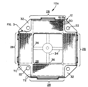
Refernng to the drawings in detail, wherein like numerals are used to
indicate like elements throughout, there is shown in Figs. 1-6 mating
connectors 10a, l Ob
constructed in accordance with one embodiment of the present invention. As
seen, each
mating connector 10a, lOb comprises a generally planar base 12 defining a
plurality of
contact-receiving apertures 14. Each contact-receiving aperture 14 receives an
appropriate
contact 16a, 16b. The apertures 14 and contacts 16a, 16b in the connectors
10a, l Ob are
arranged in a complementary manner such that each contact 16a in the connector
l0a
electrically couples to a corresponding contact 16b in the connector l Ob when
the mating
connectors 10a, lOb are coupled.
In one embodiment of the present invention, one mating connector 10a,
l Ob is electrically secured to terminals of an electrical package 18 (Fig. 5
shows connector
l Ob so coupled) while the other mating connector 10a, l Ob is electrically
secured to a
substrate 20 (Fig. 2 shows connector l0a so coupled) such as a printed circuit
board such
that the package 18 is mounted to the substrate 20 by way of both mating
connectors 10a,
l Ob. Each of the connectors 10a, l Ob may include various keying features to
ensure
alignment of the contacts 16a, 16b during mounting. In addition, the
connectors 10a, lOb
may include screw apertures 22 for receiving jack screws (not shown) to
further ensure
alignment. Such jack screws when tightened also provide motive force for
securely
coupling each pair of corresponding contacts 16a, 16b in the connectors 10a, l
Ob.
In one alternative embodiment of the present invention, the contacts 16a,
16b of one mating connector 10a, l Ob are integrally coupled to the terminals
of the
package 18 and employed to mount such package 18 directly to the other mating
connector 10a, l Ob on the substrate 20. In another alternative embodiment,
the contacts
CA 02342285 2001-03-27
y
BERG2533/C2404 - 6 - PATENT
16a, 16b of one mating connector 10a, lOb are integrally coupled to the
substrate 20 and
employed to receive the other mating connector 10a, l Ob as electrically
secured to the
package 18. Any appropriate method of electrically securing the contacts 16a,
16b of the
connector 10a, l Ob to the package 18 or the substrate 20 may be employed
without
departing from the spirit and scope of the present invention. For example, the
contacts
16a, 16b may be provided with fusible elements such as solder balls 24 or the
like and
solder-coupled to respective terminals on the package 18 or substrate 20.
Each contact 16a, 16b is constructed as a generally unitary body from a
conductive material such as KOVAR (a low coefficient of thermal expansion
(CTE)
material). However, each contact 20 could be formed from any suitable
conductive
material including a copper material, a brass material, a stainless steel
material, a gold
material, a metal alloy material, or the like. However, each contact 16a, 16b
may be
formed from any other conductive material without departing from the spirit
and scope of
the present invention. Moreover, the contacts 16a, 16b may be any appropriate
contacts
16a, 16b without departing from the spirit and scope of the present invention.
For
example, and as seen in Figs. 2 and 5, the connector l0a may have dual-beam-
type
contacts 16a and the connector l Ob may have complementary blade-type contacts
16b,
where one beam of each contact 16a is in physical contact with each side of
the blade of
each corresponding contact 16b when the contacts 16a, 16b are appropriately
mated. An
example of such contacts 16a, 16b is disclosed in International Publication
No. WO
98/15989 (based on International Application No. PCT/LTS97/18066), hereby
incorporated
by reference. As may be appreciated, by using dual-beam contacts 16a and blade
contacts
16b, as shown, contact spacing (center to center) may be about 0.05 inches or
less, with a
resulting relatively high contact density on the connectors 10a, l Ob.
The contact-receiving apertures 14 are sized to securely receive the
contacts 16a, 16b. As may be appreciated, such apertures 14 extend between
both planar
sides of the bases 12 of the connectors 10a, l Ob since the contacts 16a, 16b
received
therein must be accessible at both planar sides of the base 12. In one
embodiment of the
present invention, the apertures 14 are organized into rows such that
a.contact-insertion
device (Fig. 8) inserting contacts 16a, 16b therein inserts such contacts 16a,
16b row-by-
row. Any appropriate aperture 14 may be employed without departing from the
spirit and
CA 02342285 2001-03-27
BERG2533/C2404 - 7 - PATENT
scope of the present invention, as long as the aperture 14 is designed to and
does in fact
securely hold a received contact 16a, 16b therein. In addition, any
appropriate contact-
insertion device and method may be employed without departing from the spirit
and scope
of the present invention.
In one embodiment of the present invention, and still referring to Figs. 1-6,
the base 12 of the connector 10a, l Ob defines a generally centrally located
center aperture
26 extending therethrough. As should be appreciated, the center aperture 26 is
much
larger than any of the contact-receiving apertures 14, and in fact is not
expected to receive
any element, although an element may still be received therein without
departing from the
spirit and scope of the present invention. Preferably, the base 12 has at
least three
generally identical sectors 28, where each sector 28 is circumferentially
arranged around
the center aperture 26. In Figs. 1-6, the base 12 of the connector 10a, lOb is
generally a
square and has four such generally identical sectors 28, where each sector 28
roughly
corresponds to a side of the square. However, the base 12 may alternatively
have three,
five, six, seven, eight, etc. such sectors 28 without departing from the
spirit and scope of
the present invention. In any event, the sectors 28 generally surround and at
least partially
define the center aperture 26, and thus extend generally tangentially with
regard to such
center aperture26, as shown.
Each sector 28 defines a plurality of contact-receiving apertures 14, as
shown. As is to be expected, each contact-receiving aperture 14 in each sector
28 extends
through the base 12 in a first direction generally perpendicular to such base
12. Thus, and
as was discussed above, each contact-receiving aperture 14 can receive a
contact 16a, 16b
therein such that the received contact 16a, 16b is accessible from both planar
sides of the
base 12.
Importantly, the contact-receiving apertures 14 in each sector 28 are
organized into a plurality of rows 30, and each row 30 in each sector 28
extends along the
base 12 in a second direction with regard to center aperture 26. That is,
although rows 30
from different sectors 28 may not extend in the same direction, within a
sector all of the
rows extend in the same (second) direction. Nevertheless, such second
direction is always
the same with regard to the center aperture 26, even across different sectors
28. In one
embodiment of the present invention, and as shown in Figs. l and 4 in
particular, the
CA 02342285 2001-03-27
BERG2533/C2404 - 8 - PATENT
second direction is generally tangential with regard to the center aperture
26, where the
rows 30 are generally linear and parallel with each other. That is, the rows
30 are
generally parallel to the adjacent edge of the base 12. Of course, the second
direction may
have a different orientation with regard to the center aperture 26 without
regard to the
spirit and scope of the present invention. For example, the second direction
may be
generally radial with regard to the center aperture 26, where the rows 30 are
generally
parallel with each other and are perpendicular to the adjacent edge of the
base 12.
In one embodiment of the present invention, the contacts 16a, 16b are
generally planar in the region where such contacts 16a, 16b are secured within
corresponding contact-receiving apertures 14. Accordingly, each such contact-
receiving
aperture 14 is generally narrow at least in the dimension spanning from one
planar side to
the other planar side of a received contact 16a, 16b. Correspondingly, the
contacts 16a,
16b have an appreciable lateral extent in the region where such contacts 16a,
16b are
secured within corresponding contact-receiving apertures 14. Accordingly, each
such
contact-receiving aperture 14 extends a distance in the dimension spanning
from one
lateral side to the other lateral side of a received contact 16a, 16b, i.e .
in a third direction
in the base 12 with regard to such center aperture 26. As should be
appreciated, the third
direction is generally parallel to the base 12. In fact, in the embodiment of
the present
invention shown in Figs. 1-6, the third direction and the second direction may
be generally
identical. In such a situation, it will be appreciated that each contact-
receiving aperture 14
in each sector 28 extends along the base 12 generally tangentially with regard
to the center
aperture 26. However, the third direction may differ with regard to the second
direction
without departing from the spirit and scope of the present invention. For
example, the
third direction may be generally perpendicular to the second direction.
As may be appreciated, the center aperture 26 of the connector 10a, l Ob of
the present invention allows such connector 10a, l Ob to be able to
effectively
accommodate and relieve mechanical and thermal stresses, among other things.
That is,
the center aperture imparts a relatively large degree of flexibility to the
connector 10a,
l Ob. Accordingly, mechanical and thermal activity experienced by the
connector 10a, l Ob
will be less likely to warp or crack the connector 10a, lOb, and it is less
likely, that
CA 02342285 2001-03-27
BERG2533/C2404 - 9 - PATENT
repeated cycles of mechanical or thermal stresses will act to move contacts
16a, 16b out of
electrical connection with corresponding contacts 16a, 16b and/or terniinals.
In one embodiment of the present invention, in an effort to even more
effectively accommodate and relieve mechanical and thermal stresses on the
connector
10a, l Ob, among other things, the base 12 of such connector 10a, l Ob is
further provided
with flexible corners 32. More particularly, the base 12 has a plurality of
such corners 32
such that each sector 28 meets an immediately adjacent sector 28 at one of the
corners 32.
The base 12 also has a pair of opposing generally planar sides, each corner 32
has a first
general side-to-side thickness TC, and each sector 28 has a second general
side-to-side
thickness TS greater than the first thickness TC. In fact, the first thickness
TC may be as
thin as the manufacturing process allows, although other thicknesses are
possible and are
within the spirit and scope of the present invention. As should be evident,
then, the
corners 32 provide the base 12 with an additional degree of flexibility over
and above that
provided by the center aperture 26 to relieve physical and thermal stresses to
the base 12
of the connector 10a, l Ob. As seen, the corners 32 may define the screw
apertures 22,
although such screw apertures 22 may reside elsewhere without departing from
the spirit
and scope of the present invention.
The base 12 of the connector 10a, l Ob may be formed in any appropriate
manner from any appropriate non-conductive material without departing from the
spirit
and scope of the present invention. In one embodiment of the present
invention, the base
12 is injection molded from a non-conductive material such as a ceramic
material, a
polymeric material such as a liquid crystal polymer, a thermosetting resin
(e.g., FR4) or an
elastomeric material. In particular, and as best seen in Figs. 1 and 7, an
injection mold is
provided that defines the base 12, where the injection mold includes a gate
structure 34 at
the center aperture 26 of the to-be-molded base 12 (step 701). Of course, the
injection
mold is appropriately formed to include all necessary features of the base 12,
including the
sectors 28, the center aperture 26, the screw apertures 22, the corners 32,
the contact-
receiving apertures 14, etc.
As may be appreciated, the non-conductive material.that is to form the base
12 is injected into the injection mold through the gate structure 34 at the
center aperture
26 of the to-be-molded base 12 in a manner such that the injected material is
generally
CA 02342285 2001-03-27
BERG2533/C2404 -10 - PATENT
evenly distributed into each sector 28 of the base 12 (step 703). In one
embodiment of the
present invention, and as seen, the gate structure 34 includes an egress 36
adjacent each
sector 28 of the base 12 such that the injected material is generally evenly
distributed from
each egress 36 into the adjacent sector 28 of the base I2. Of course, multiple
egresses 36
may also be employed for each sector 28, as may be alternate egress 36 and
gate structure
34 designs, all without departing from the spirit and scope of the present
invention.
Once properly injection molded by way of the injection mold and the gate
structure 34 thereof, the molded base is removed from the injection mold (step
705). Of
course, various finishing operations may be performed, such as for example,
trimming of
excess injected material and smoothing thereat. Overall, injection molds,
injection
molding, and finishing operations after injection molding are generally known
to the
relevant public. Accordingly, further details regarding same need not be
provided herein.
As should now be appreciated, by centrally injection molding the base 12
of the connector 10a, l Ob from the center aperture 26 of the to-be-molded
base 12, the
injected material evenly expands into the mold past the many mold features and
thereby
completely fills the mold to faithfully render the base 12 within the mold.
Moreover, by
such even expansion from multiple egresses 36 at a central location unwanted
voids in the
base 12 are minimized if not eliminated, and the injection material under
proper
conditions does not solidify prior to completely filling the mold.
Now that the base 12 has been formed, such base 12 must be loaded with
the contacts I6a, 16b. In one embodiment of the present invention, and
refernng now to
Figs. 8 and 9, such contacts I6a, I6b are loaded by way of a loading apparatus
38
including a platform 40 rotatable on an axis and a contact insertion device 42
adjacent
thereto. The finished base 12 sans the contacts 16a, 16b is appropriately
mounted to the
platform 40 such that the base 12 is generally perpendicular to the axis and
the axis is
coincident with the center aperture 26 (step 901). Importantly, the adjacent
contact
insertion device 42 is positioned over the base 12 on the platform such that
the device 42
has a field of view comprising a circumferential portion of the platform 40.
That is, the
contact insertion device 42 upon being appropriately moved is capable of
reaching any
area within such circumferential portion.
CA 02342285 2001-03-27
BERG2533/C2404 - 11 - PATENT
As should now be appreciated, the rotatable platform 40 and the base 12
mounted thereto are rotated to a first position wherein the field of view of
the contact
insertion device 42 coincides with a first one of the sectors 28 of the base
12 (step 903).
In such first position, the contact insertion device 42 inserts a contact 16a,
16b into each
contact-receiving aperture 14 of the first one of the sectors 28 (step 905).
The rotatable
platform 40 and the base 12 mounted thereto are then rotated to a second
position wherein
the field of view of the contact insertion device 42 coincides with a second
one of the
sectors 28 of the base 12 (step 907). In such second position, the contact
insertion device
42 inserts a contact 16a, 16b into each contact-receiving aperture 14 of the
second one of
the sectors 28. It should now be understood that the rotating and inserting
steps are
repeated until each sector 28 of the base 12 is filled with contacts 16a, 16b.
For the four-sector base 12 shown in Figs. 1-6, the rotating and inserting
steps are performed four times. Preferably, the rotation from position to
position is about
90 degrees, although other angles of rotation may also be employed without
departing
from the spirit and scope of the present invention. Overall, loading apparati
38 for
loading contacts 16a, 16b into a base 12 of a connector 1 Oa, l Ob and methods
for using
such loading apparati 38 are generally known to the relevant public.
Accordingly, further
details regarding same need not be provided herein.
As should now be appreciated, by employing a base 12 with a center
aperture 26 and sectors 28 circumferentially surrounding such center aperture
26, and by
filling the base 12 sector-by-sector, where the rows 30 of contacts 16a, 16b
in each sector
28 are presented in the same manner to the contact insertion device 40, all of
the contact
receiving apertures are easily reachable by such contact insertion device 40,
and such
insertion may take place in an expeditious manner.
Referring now to Figs. 10 and 11, a pair of connectors 100a, 100b are
shown in accordance with another embodiment of the present invention. Such
connectors
100a, 100b are similar to the connectors 10a, lOb of Figs. 1-6 and therefore
need not be
described in detail. In pertinent part, the base 12 of the connector 100a,
100b defines a
generally centrally located center aperture 26, and the base 12 has four
generally identical
sectors 28 circumferentially arranged around the center aperture 26. Each
sector 28 in the
connector 100a, 100b is organized into a plurality of rows 30, where each row
30 in each
CA 02342285 2001-03-27
BERG2533/C2404 - 12 - PATENT
sector 28 extends generally tangentially with regard to such center aperture
26. Notably,
though, each sector 28 and the rows 30 therein extends into an area reserved
as a corner 32
in the connectors 10a, l Ob. In addition, the base 12 of the connector 100a,
100b does not
include screw apertures 22 for jack screws or the like.
The base 12 of the connector 100a, 100b may be formed in substantially
the same manner as the base 12 of the connector 10a, l Ob, i.e., by way of a
centrally
located gate structure 34 such as that shown in Fig. 1. Moreover, the contacts
16a, 16b
may be loaded into the base 12 of the connector 100a, 100b in substantially
the same
manner as into the base 12 of the connector 10a, lOb, i.e., by way of the
loading apparatus
38 of Fig. 8.
In the foregoing description, it can be seen that the present invention
comprises a new and useful electrical connector 10a, l Ob, 100a, 100b for use
in
connection with an electrical package 18 and/or a substrate 20. It should be
appreciated
that changes could be made to the embodiments described above without
departing from
the inventive concepts thereof. It should be understood, therefore, that this
invention is
not limited to the particular embodiments disclosed, but it is intended to
cover
modifications within the spirit and scope of the present invention as defined
by the
appended claims.