Note: Descriptions are shown in the official language in which they were submitted.
CA 02342538 2001-04-03
JP Delavaux 28-4
OPTICAL FIBER TRANSMISSION SYSTEM ~i~VITH POLARIZATION
MULTIPLEXING TO REDUCE STIMULATED BRILLOUIN SCATTERING
Technical Field
The present invention relates to an optical fiber transmission system with
reduced levels of stimulated Brillouin scattering (SBS) aa:~d, more
particularly, to the use
of polarization multiplexing of the pump signal to reduce. the effects of SBS.
Background of the Invention
In long distance optical fiber transmission systems, it is desirable to launch
as
high an optical power as possible, enabling the lightwave signals to be
transmitted
without the need for additional components such as repeavters and amplifiers,
which
increase the cost of communication systems. However, t:he combination of high
powered, narrow linewidth optical sources with low-loss single mode
transmission fiber
opens the possibility of signal degradation and increased bit error rates,
attributable to a
host of nonlinear fiber-related phenomena that have been previously considered
inconsequential. These nonlinear phenomena include stimulated Brillouin
scattering
(SBS), stimulated Raman scattering, self phase modulation and, if two or more
optical
channels are involved, cross-phase modulation and four-wave mixing.
Stimulated Brillouin scattering within a fiber results from photons being
scattered by localized refractive index variations induced by acoustic waves.
These
refractive index variations are caused, in particular, by ultrasonic
vibrations in the glass
lattice that makes up the fiber core. Furthermore, owing t:o the dependence of
refractive
index on light intensity in the nonlinear regime, the presence of intense
lightin the fiber
will also induce lattice vibrations, which in turn induce sound waves that
then scatter
more light. Ultimately, light from an intense forward propagating signal
(referred to as
a "pump" signal) can provide gain for a backward propagating or "Stokes"
signal. This
scenario is a classical description of SBS. SBS threshold power (denoted as
PsBS) is
arbitrarily defined as the level of input optical pump signal power (Pp",rp)
at which the
power of the backward Stokes signal (Pstokes) becomes equal to Pp"",p at the
fiber input.
CA 02342538 2001-04-03
JP Delavaux 28-4 2
SBS threshold power increases with the linewidth of the; light being
propagated along a
fiber. For this reason, concern over the adverse effects of SBS was minimal -
until the
introduction of narrow linewidth laser sources. As narrow linewidth sources
become
more readily available, and as such lasers are likely to b~e the optical
source of choice
for future optical fiber transmission systems, SBS has th.e potential for
significantly
contrihuting to signal degradation at relatively low input: power levels.
To date, several techniques have been demonstrated to suppress the SBS in
optical transmission systems. In general, these techniques fall into two main
categories:
(1) modifications ofthe fiber media to reduce SBS; or (a>.) modifications of
the laser
source to alter the linewidth. In the first category, it is possible to
influence the
refractive index (and acoustic velocity) along the longitudinal direction of
the fiber, thus
varying the Brillouin gain profile along the fiber. This variation avoids the
accumulation of gain within a small bandwidth and resul',ts in a broader gain
profile and
high SBS threshold. However, this fiber modification approach is not
practical, since it
is relatively difficult to introduce these effects into the fiber as it is
manufactured and,
more importantly, cannot be used to reduce SBS on the extensive embedded base
of the
optical fiber network already in place.
The alternative solution of modifying the laser source to affect the level of
SBS
has been found to be more practical and can be used with existing optical
fiber systems.
This technique is based on the property of broadening the laser linewidth by
means of
modulation. U.5. Patent 5,329,396, issued to D.A. Fishman et al. on July 12,
1994,
discloses one exemplary prior art arrangement which impressed FM modulation on
the
laser bias current to increase the linewidth. This direct FM approach, by
using a dither
signal, provides a relatively large frequency excursion (on the order of, for
example,
lOGHz). By means of this technique, the SBS threshold has been increased as
much as
lSdB. However, impressing an FM signal on the laser bias has been found to
also result
in substantial AM (defined as "residual AM"), degrading system performance.
Alternatively, external phase modulation (PM) can be us<;d to broaden the
laser
linewidth. US Patent 5,166,821 issued to D. Huber on November 24, 1992
discloses one
CA 02342538 2005-03-09
3
such PM arrangement. However, in aptical transmission systems, this external
PM
technique typically degrades the dispersion characteristics of the signal due
to an
excessive increase in the linewidth of the laser source.
Thus, a need remains in the art for an arrangement that reduces SBS without
introducing other types of signal degradation in the optical transmission
system.
Summary of the Iuventioh
The need remaining in the art is addressed by the present invention, which
relates
to an optical fiber transmission system with reduced levels of stimulated
Brillouin
scattering (SBS) and, more particularly, to the use of polarization
multiplexing of the
pump signal to reduce the effects of SBS.
In accordance with the present invention, a laser optical output is split into
orthogonal polarizations (denoted "S" and "P") and allowed to propagate along
two
different signal paths. A time delay (~) is introduced along one signal path
in order to
break the coherence between the signals. One polarization is also frequency-
shifted (0f)
with respect to the other. In a preferred embodiment, an acousto-optic (A-O)
modulator
is used to introduce the frequency shift. These two incoherent, frequency-
shifted
orthogonal signals are then re-combined onto a common signal path. Since SBS
is a
polarization-dependent phenomenon, by splitting the optical signal as defined
above, the
presence of SBS on each polarization is significantly reduced.
An advantage of the arrangement of the present invention is the reduction of
various other polarization-dependent phenomena in the optical system (e.g.,
polarization-dependent losses, spatial hole burning).
In a preferred embodiment of the present invention, the polarization
multiplexing
can be combined with either one or both of the prior art FM and PM SBS
reduction
techniques to achieve even greater reductions in this effect.
In accordance with one aspect of the present invention there is provided a
method
for suppressing stimulated Brillouin scattering in an optical transmission
system, the
method comprising the steps of a) providing a laser source for generating an
optical
CA 02342538 2005-03-09
3a
signal O having a relatively narrow linewidth; b) splitting the optical signal
into a first
signal component and a second signal component, the signal components being of
orthogonal polarization states; c) introducing a predetermined time delay ~iD
into the
first signal component; d) introducing a predetermined frequency shift Of into
the
second signal component; e) combining the time-delay first signal component
and the
frequency-shifted second signal component to form a polarization multiplexed
optical
signal with increased linewidth; and f) coupling said polarization multiplexed
optical
signal into the optical transmission system output fiber.
In accordance with another aspect of the present invention there is provided
apparatus for communicating optical signals over an optical fiber comprising a
laser
source for providing an optical output signal; a polarization beam splitter
coupled to the
laser for dividing the optical output signal into a first signal component and
a second
signal component, the signal components being orthogonally polarized, and
coupling the
first and second signal components into separate first and second signal
paths; a delay
element coupled to said first signal path for introducing a predetermined time
delay din
into the first orthogonally polarized signal component; a frequency shifting
element
coupled to said second signal path for introducing a predetermined frequency
shift Of into
the second orthogonally polarized signal component; and a polarization beam
combiner
responsive to the time-delayed first orthogonally polarized signal component
and the
frequency-shifted second orthogonally polarized signal component.
Various other features and advantages of the present invention will become
apparent during the course of the following discussion and by reference to the
accompanying drawings.
CA 02342538 2001-04-03
JP Deiavaux 28-4 4
Brief Description of the Drawings
Referring now to the drawings,
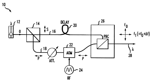
FIG. l illustrates an exemplary polarization multiplexing optical transmitter
of
the present invention for reducing SBS;
FIGS. 2A - 2B contains graphs of intensity variation, with respect to time and
frequency, for the arrangement of the present invention as illustrated in FIG.
l;
FIG. 3 illustrates an alternative embodiment of the present invention,
incorporating prior art SBS suppression techniques with the polarization
multiplexing
scheme of the present invention;
FIG. 4 is a graph depicting SBS thresholds as a function of input power for a
variety of prior art applications and arrangements of the present invention;
FIG. 5 is a graph of SBS spectra, as a function of frequency for a prior art
CW
signal and alternative arrangements using polarization mulltiplexing in
accordance with
the present invention;
FIG. 5 is a graph of SBS spectra for arrangements including frequency
dithering
with the inventive polarization multiplexing technique;
FIG. 7 illustrates an alternative embodiment of the present invention,
utilizing a
delay element and AOM, in cooperation with a pair of electro-optic modulators
(a
separate EOM disposed in each arm);
FIGS. 8A - 8C shows the intensity variation with respect to time and frequency
for the arrangement of FIG. 7;
FIG. 9 illustrates yet another embodiment of the present invention, utilizing
a
switchable AOM responsive to both polarization states, to control the
polarization state
of the output signal;
FIG. 10 illustrates an embodiment of the present invention wherein the input
signal is first split into two components and each component separately
polarization
multiplexed;
FIG. 11 is a graph of the signal intensity, as a function of frequency, for
the
arrangement of FIG. 10; and
CA 02342538 2001-04-03
JP Delavaux 28-4 5
FIG. I2 is an alternative embodiment of the present invention utilizing a
polarization modulator, coupled to the output of the laser source, to control
the
polarization state of the optical output signal from the transmitter.
Detailed Description
S FIG. 1 illustrates an exemplary polarization multiplexed optical input
signal
arrangement 10 formed in accordance with the teachings of the present
invention.
Arrangement 10 includes a laser source 12, which can comprise any conventional
type
of semiconductor laser (for example, a distributed feedback (DFB) laser) with
a
wavelength chosen in a desirable optical communication window, such as 1300nm
or
ISSOnm. The optical signal O from laser source 12 is subsequently applied as
an input
to a power splitting component 14 (e.g., a polarization be;~m splitter or
coupler) which
functions to split optical signal O into orthogonal components, denoted S and
P in FIG.
l, where these orthogonal components are launched onto separate signal paths
16 and
18. In the particular embodiment as shown in FIG. l, the S component is
coupled to
1 S signal path 16 and the P component is coupled to signal path 18. It is to
be noted that
signal paths 16 and 18 may comprise polarization-maintaining optical fibers,
integrated
waveguides, or any other media suitable for supporting the propagation of
polarized
optical signals. Thereafter, one of the polarized components (in this case,
the S
component) is passed through a delay element 20, so as to break the coherence
(in time)
between the S and P components by introducing a predetermined delay, denoted
~iD,
onto one of the components . When using optical fiber, delay element 20 may
simply
comprise an additional length L of optical fiber.
The remaining polarized signal component, in this example the P component, is
applied as an input to a frequency-shifting device 22, in this case an acousto-
optic
2S modulator (AOM). An external RF source 24 is used to supply a frequency
shift signal
rf to AOM 22, resulting in a predetermined frequency shift ~f impressed upon
polarized
component P. The time-delay component S and the frequency-shifted component P
are
then applied as separate inputs to a polarization beam combiner 26, which
functions to
CA 02342538 2001-04-03
JP Detavaux 28-4 6
couple the signals together and provide them as the output of optical input
signal
arrangement 10, along an output signal path 28.
In accordance with the present invention, therefore, the introduction of both
incoherence in the time domain and a shift in the frequency domain results in
significantly increasing the Brilloiun threshold for each polarization (which
remain
independent of each other). Additiona.ily, the polarization multiplexing
technique of the
present invention, by providing "depolarization" of the input signal, will
also result in
reducing various other polarization-dependent impairments (such as, for
example,
polarization-dependent losses and polarization hole burni:ng).
FIG. 2 illustrates intensity variations associated with arrangement 10 of FIG.
1.
FIG. 2A illustrates the separation of intensity along the orthogonal S and P
components,
as well as the time delay diD provided by delay element 20 on signal component
S.
FIG 2B is a frequency domain diagram of the signal intensity, showing in
particular the
frequency shift ~f between the S and P components supplied by AOM 22.
As mentioned above, it is possible to use the polarization multiplexing
technique
of the present with either of the prior art FM and PM techniques to achieve
even greater
SBS suppression. FIG. 3 illustrates an exemplary embodiment of the present
invention
including polarization multiplexer 10, as shown in FIG. l, in combination with
a pre-
multiplexer element 30 for providing either one of FM and PM (the phase
modulation
elements are illustrated in phantom in FIG. 3, denoting this as an alternative
to FM).
Referring to FIG. 3, laser source 12 is illustrated as being directly coupled
to an FM
source 32, which functions to apply a dither signal d directly to the laser
bias. In one
embodiment, dither signal d may comprise a 50mV sinusoidal signal at a
frequency of
approximately 104MHz. The presence of the dither signal'. provides large
frequency
excursions and can increase the SBS threshold by an additional lSdB. As an
alternative, a phase modulation arrangement comprises an electro-optic
modulator
(EOM) 34, such as a Mach-Zehnder interferometer, and an external drive source
3G.
Drive source 36 is used to supply an RF signal, denoted rf; to control the
phase
CA 02342538 2001-04-03
JP Delavaug 28-4 7
modulation within EOM 34. It is known that the linewidth broadening supplied
by such
a phase modulation arrangement is proportional to both the; frequency and
modulation
index of the RF signal, and is also on the order of lSdB. In either the FM or
PM case,
the laser output is subsequently applied as an input to power splitting
component 14,
where this signal is then processed in the same manner as described above in
association with FIG. 1.
The improvement in laser threshold by utilizing these techniques is evident
from
the graph of FIG. 4, which plots the backscattered (SBS threshold) power as a
function
of the input power. The "linearly" polarized plots A and B correspond to
arrangements
which do not utilize the polarization suppression arrangem<~nt of the present
invention,
plot A associated with a conventional prior art (CW) arrangement and pint B
with an
arrangement including FM dither. Also shown, for both thc~ CW and FM cases
(plots C
and D, respectively) are the results from utilizing polarization multiplexing
and
incoherence (that is, with a time delay but no frequency shifting). An
increase in SBS
threshold of approximately 1 dB is shown for each of. these plots. With the
addition of a
frequency shift (referring to plots E and F), an additional 3clB of threshold
power level
is obtained.
FIGS. 5 and 6 illustrate the resultant SBS spectra associated with various
embodiments of both the prior art and the present invention. In particular,
FIG. 5
includes a set of SBS spectra under the following conditions: (a) a
conventional laser
source; (b) a "depolarized" optical source including the tim<; delay of the
present
invention; and (c) a "depolarized" optical source including both a time delay
and
frequency shift of the present invention, where the plot in (c) is obtained
for collinear
signals (linearity achieved by replacing polarization beam combiner 26 with a
conventional 3dB coupler and adjusting the polarizations to be parallel). In
both cases
associated with the present invention (plots (b) and (c)), the SBS spectra now
includes
extra frequency components, thus raising the SBS threshold of the transmitter
arrangement. Similarly, the plots of FIG. 6 illustrate the SBS spectra when FM
CA 02342538 2001-04-03
JP Deiavaux 28-4 g
dithering is impressed on the laser source. Obviously, the dithering results
in adding
even more frequency components to the SBS spectra, further raising the SBS
threshold.
An alternative embodiment 40 of the present invention is illustrated in FIG.
7.
In this case, a 3dB coupler 42 is used to split output optical signal O from
laser source
12 into two relatively equal power components, denoted OI and 02 in FIG. 7. As
with
the previous embodiment discussed above in association with FIG. 1, one
component
(in this case, OI, is subjected to a time delay ~zD and the remaining
component (D~) is
frequency shifted by AOM 22 by a predetermined amount 4f. In this embodiment,
a
pair of electro-optic modulators 44, 46 are included, one on each arm of
arrangement
40. EOMs 44,46 are used to supply the input data stream to the transmitter,
instead of
directly providing the data D on the bias current supplied to laser source 12.
In one
embodiment data signal D and is complement D' are applied as inputs to EOMs 44
and
46, respectively. Alternatively, two different data streams, DI and DZ may be
simultaneously transmitted using this arrangement. Orthog;onality between the
signals
in provided by including a polarization rotator device 48 in one signal path,
as shown in
FIG. 7. Thereafter, the two polarized components are re-joined in polarization
beam
combiner 26 to form the output of arrangement 40.
FIG. 8 contains various graphs illustrating the aspects of arrangement 40 as
shown in FIG. 7. In particular, FIG. 8A illustrates the intensity variation,
with respect
to time, for the two signal components subsequent to the one component passing
through the polarization rotator device 48. If EOMs 44, 46 are driven by the
same
(complementary) data, when one state-of polarization (SOP) is "on", the other
is "off',
and vice versa. This arrangement thus provides the same amount of optical
power to
exist at any one time. The delay of the present invention, introducing the
time delay
DiD as shown in FIG. 8A, breaks the coherence between the data streams. A
possible
intensity variation for this arrangement is shown in FIG. 8B, where the
resultant power
is shown as varying between 0 and 2P as a function of time. The frequency
domain
CA 02342538 2001-04-03
JP Delavaux 28-4 9
intensity is illustrated in FIG. 8C, with the two depolarized signals
illustrated as also
separated in frequency by the predetermined shift ~f introduced by AOM 22.
Yet another embodiment 50 of the present invention is illustrated in FIG. 9.
As
before, the optical output O from laser source 12 passes through polarization
beam
splitter 14 to form the orthogonal components S and P, where component S is
then
subjected to a time delay ~zD. These two components arcs then applied as
separate
inputs to an acousto-optic modulator 52, where modulator 52 is driven by an
external
RF source 54, as controlled by a data source 56. In particular, AOM 52 is
controlled
such that when the signal from data source 56 is a first state (e.g., a logic
"I"), AOM 52
I O is positioned to provide as an output the time-delayed connponent S, and
when the signal
from data source 56 is a second state (e.g., a logic "0"), A.OM 52 is
positioned to
provide as an output component P, where the action of AlJM 52 will impress a
phase
shift between the components.
Additional spectrum broadening in accordance with the present invention can be
I S realized by~using an arrangement such as that illustrated in FIG. I0. As
shown, optical
source 60 includes laser source I2, where the optical output O from source 12
is first
split into two (relatively equal) components, denoted as OI and O2, within a
3dB
coupler 62. Output signal OI is thereafter applied as an input to a first
polarization
beam splitter 64 to form orthogonal components Sl and Pl. In similar fashion,
signal 02
20 is applied as an input to a second polarization beam splitte:r 66, forming
orthogonal
components S2 and P2. The components SI and P~ are processed in the manner
discussed above, using a first delay element 68 and AOM 70 to introduce both
incoherence and a frequency shift between the components. The components are
then
re-combined in a polarization combiner 72 and provided a;s a first output
along a signal
25 path 74.
In this particular embodiment, components S2 and i°2 are both time
delayed, as
shown in FIG. 10, where component S2 passes through a second delay element 76
and
component P2 passes through a third delay element 78. The actual values of
each time
CA 02342538 2001-04-03
JP Delavaux 28-4 10
delay, OzDi, dig, and DiD3, are chosen so as to be slightly different,
ensuring that each
component is incoherent with respect to all other components. In order to also
provide
different, additional frequency shifts a pair of AOMs 80 anal 82 are utilized
with
components SZ and PZ to provide the necessary, unique frequency shifts for
each
component. The time-delay, frequency-shifted components S2 and PZ are
thereafter re-
combined in a polarization combiner 84 and applied as inputs to a signal path
86.
Referring to FIG. 10, the various components propagating .along signal paths
74 and 86
are then applied as inputs to a coupler 88 to form the final output signal
from
arrangement 60.
FIG. 11 illustrates the spectral power density distribution, with respect to
polarization state, for arrangement 60 of FIG: 10. Iilustrate;d in this
diagram in
particular, are the different, unique frequency shifts introduced by AOMs 70,
80 and 82.
FIG. 12 illustrates yet another embodiment 90 of the present invention,
utilizing
a separate polarization modulator 90 to provide both polari::ation diversity
and
frequency dithering to the optical signal. As before, a laser source 12 is
used to provide
an optical output signal O. An external modulator 94 is coupled to
polarization
modulator 92 and used to control the output polarization state from
polarization
modulator 92. In this arrangement, when modulator 94 transmits a first value
(e.g.,
logic "1") to polarization modulator 92, the output will be an S-polarized
signal, and
when modulator 94 transmits a second value (e.g., logic "0''') to polarization
modulator
92, the output will be a P-polarized signal. The output from polarization
modulator 94
is then provided as an input to a polarization beam splitter 96, which
functions to
direction the S component along a first signal path 98 and the P component
along a
second signal path 100. The coherence between the two components is broken by
including a delay element 102 along signal path 98. As with the other
embodiments
discussed above, a frequency shift between the components is introduced by an
acousto-
optic modulator 104 inserted along the P-polarized signal path 100. The S and
P
CA 02342538 2001-04-03
JP Delavaux 28-4 11
components are thereafter combined in a polarization beam combiner 106 to form
the
final, polarization-multiplexed output signal.
It is to be understood that the various embodiments as discussed above are to
be
considered as exemplary only, there exist many other possible arrangements for
S supplying polarization multiplexing onto an optical transmiission signal so
as to
suppress SBS in accordance with the present invention. Further, as mentioned
above,
any of the possible arrangements of the present invention may be embodied as
discrete
components (such, for example, optical fibers as the signal paths), integrated
arrangements (using, for example, optical waveguides), or any hybrid sort of
arrangement using a component of both discrete and integrated components. In
general,
the spirit of the present invention is to be limited only by the scope of the
claims as
appended hereto.