Note: Descriptions are shown in the official language in which they were submitted.
CA 02342548 2001-03-30
-
121831D
CROSSPOINT SWITCH PROTECTION
FIELD OF THE INVENTION
The present invention relates to a crosspoint switch, and in particular to an
apparatus and a method suitable for providing alternative pathways through the
switch in the event of a failure of a switching element. These alternative
pathways
have the potential to be engaged automatically and/or remotely.
BACKGROUND OF THE INVENTION
Communications networks are moving towards becoming all optical (photonic)
networks, incorporating photonic (optical) switching in which optical signals
are
switched directly rather than converted to electrical signals, switched
electrically,
then converted back to optical signals for re-transmission. Photonic switches
may
be used to switch wavelength division multiplexed (WDM) signals as a group, or
the WDM signals may be demultiplexed outside the switch and switched
individually as channels, or as groups of channels as desired. Photonic
switches
are fabricated using a range of technologies and frequently employ a
crosspoint
(crossbar) architecture. In such architectures light from an input port may
traverse
a number of switching elements. At each switching element the light may be
switched and directed towards an associated output port or alternatively pass
though to the next switching element. Once the light has been directed towards
an
output port it may traverse more switching elements which, in most
CA 02342548 2001-03-30
-2-
implementations, must remain inactive so as not to block or disrupt the light
path
before it reaches its output port
For example, a recently developed photonic switch using Micro Electro -
Mechanical systems (MEMS) technology is described in "Free - Space Micro
Machined Optical Switches for Optical Networking" by LY Lin et al, IEEE
Journal of
Selected Topics in Quantum Electronics, Vol. 5 No.1, Jan/Feb 1999; which is
incorporated herein by reference. Such MEMS switches typically use moveable
mirrors to re-direct optical paths within the switch in order to complete an
optical
signal or channel connection across the switch.
Figure 1 shows a schematic diagram of a typical MEMS photonic switch 100. The
switch 100 is bi-directional, but for simplicity is assumed to comprise 4
inputs in the
form of optical fibres 112, 114, 116 & 118, and 4 outputs which are also
optical
fibres 122, 124, 126 & 128. Each input and output has an associated lens 104
which collimates the beams from the inputs and focuses the beam at the
outputs.
Such a switch is generically referred to as a 4x4 switch (number of inputs x
number
of outputs).
The switch 100 is a crosspoint (cross bar) switch, having a switching element
(here, a mirror, 106) located at each of the points at which optical signals
emitted
from the input fibres would cross with optical signals emitted from the output
fibres.
The switch 100 thus has a four by four array of mirrors106 mounted on a
surface
102.
In this particular switch, each mirror may be moved between two stable
positions.
Figures 2a and 2b illustrate these positions. Figure 2a shows the mirror in
the
inactivated position 106a, where the mirror is flat i.e. substantially
parallel to the
CA 02342548 2001-03-30
-3-
surface 102. Figure 2b shows the mirror having been raised to the activated or
upright position 106b, substantially perpendicular to the surface 102. This
activation may be performed by a variety of means e.g. by micro actuators
causing
the mirror to be rotated about the hinges 108. The mirrors are typically
formed of
materials such as polysilicon, the reflectivity of which is increased by
providing a
reflective coating 107 such as gold. In the inactivated state, it is typical
for the
relatively non-reflective surface 109 of the mirror to lie adjacent to the
surface 102,
so that the reflective coating 107 does not contact the surface 102.
Figure 1 shows a typical operation of the switch 100. By raising the
appropriate
mirrors, an optical signal from each of the inputs 112, 114, 116 & 118 is
directed to
a respective output 128, 126, 122 & 124. For instance, an optical signal
originating
from input fibre 112 is formed into a collimated beam 132 by lens 104. The
beam
132 then reflects off the front reflective surface 107 of a raised mirror 106b
into a
further lens 104 which focuses the beam 132 into the output fibre 128. It will
be
appreciated that by appropriate control of the array of mirrors 106, any one
of the
signals originating from the inputs 112, 114, 116 & 118 can be switched into
any
one of the outputs, 122, 124,126 & 128.
In any system switching information, it is desirable to provide alternative
pathways
for the information in the event that the original pathway "fails" and is
unable to
transmit the signals as desired. Such alternative pathway provision is
commonly
referred to as "protection" when these pathways may be engaged remotely and/or
automatically.
It will be appreciated that a failure in any of the internal switching
elements (mirrors
106) would impair the functionality of the switch. For instance, any of the
mirrors
could be jammed in either the raised 106b or flat 106a position, and this
would
CA 02342548 2001-03-30
-4-
prevent a connection between the input and output corresponding to that
mirror. In
addition a mirror which is jammed in the raised position has the potential to
prevent
a connection between the associated input and another output and between
another input and the associated output. This is because the raised mirror may
act
as a block to such light paths.
The present invention aims to address such problems.
SUMMARY OF THE INVENTION
In a first aspect, the present invention provides a crosspoint switch
comprising N
primary inputs, M primary outputs and an array of (N+X) x (M+X) switching
elements, where M, N and X are all positive integers, the additional switching
elements in said array being arranged to provide alternative connectivity
between
said inputs and outputs.
A typical crosspoint switch having N inputs and M outputs will have an array
of N x
M switching elements. By providing the additional switching elements in the
array,
it becomes possible to provide alternative connectivity between the inputs and
outputs to compensate for any failures in the part of the array normally
utilised for
switching.
Preferably, said switch is a photonic switch. Photonic switches can have
switching
elements such as reflective surfaces (mirrors), refractive media, or
interferometers.
CA 02342548 2001-03-30
-5-
Preferably, said additional switching elements comprise at least one column at
an
outermost edge of the array, and at least one row at an outermost edge of the
array.
Preferably, the additional switching element located at the intersection of
each of
said row and said column is located in a fixed position so as to redirect
incident
signals in a predetermined manner. Such a switching element can act to
redirect
an incident signal from said row along said column, or from said column along
said
row.
Alternatively the switch can further comprise X additional inputs and X
additional
outputs, each of said additional outputs being transmissively connected to a
respective additional input.
Preferably, said switch is a photonic switch, and said additional outputs are
connected to said additional inputs by an optical fibre or other form of
optical wave-
guide.
Optionally, at least one of said additional outputs is coupled to a tap for
the
monitoring of signals passing through said output.
Preferably, N = M.
Preferably, X = 2. If X = 2, or any even number, protection can be provided
for one
or more switching elements that fail in the active position and act to block
signals.
Preferably, said array is substantially rectilinear.
In another aspect the present invention provides a node for a
telecommunications
network comprising a crosspoint switch comprising N inputs, M outputs and an
array of (N+X) x (M+X) switching elements, where M, N and X are all positive
CA 02342548 2001-03-30
-6-
integers, the additional switching elements in said array being arranged to
provide
alternative connectivity between said inputs and outputs.
In another aspect the present invention provides a transmission system
comprising
a transmitter and a receiver, and a transmission line connecting the
transmitter to
the receiver, the system further comprising a crosspoint switch comprising N
inputs, M outputs and an array of (N+X) x (M+X) switching elements, where M, N
and X are all positive integers, the additional switching elements in said
array being
arranged to provide alternative connectivity between said inputs and outputs.
In a further aspect the present invention provides a method of operating a
crosspoint switch comprising N inputs, M outputs and an array of (N + X) x (M
+ X)
switching elements, where N, M and X are all positive integers, the method
comprising detecting that switching element has seized to function correctly;
and
providing control signals to the switching elements for configuring the
switching
elements to provide the same connectivity as the incorrectly functioning
switching
element.
Preferably, said switch is a photonic switch arranged to switch optical
signals, the
method further including the step of providing control signals to the
switching
elements for configuring the switching elements so as to ensure that no
optical
signals are blocked by the incorrectly functioning switching element.
In another aspect, the present invention provides a computer program arranged
to
perform the method of a method of operating a crosspoint switch comprising N
inputs, M outputs and an array of (N + X) x (M + X) switching elements, where
N,
M and X are all positive integers, the method comprising detecting that
switching
element has ceased to function correctly; and providing control signals to the
CA 02342548 2001-03-30
7
switching elements for configuring the switching elements to provide the same
connectivity as the incorrectly functioning switching element.
Preferably, said computer program is stored on a machine readable medium.
BRIEF DESCRIPTION OF DRAWINGS
In order that a greater understanding of the invention can be obtained,
embodiments of the invention will now be described with reference of the
accompanying drawings, by way of example only and without intending to be
limiting, in which:
Figure 1 shows a typical MEMS switch arrangement (PRIOR ART);
Figures 2a and 2b show respectively a mirror from the switch of Figure 1 in
the
inactivated state and the activated state (PRIOR ART);
Figure 3 shows a photonic switch according to a first embodiment of the
present
invention;
Figure 4 shows an alternative configuration of the switch of Figure 3; and
Figure 5 shows a photonic switch according to a second embodiment of the
present invention.
DETAILED DESCRIPTION OF PREFERRED EMBODIMENTS
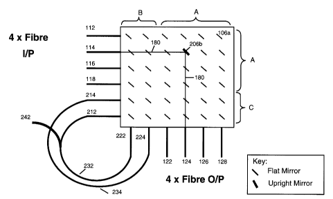
Figure 3 shows a photonic switch of similar construction principles to that
show in
in Figure 1, although the focusing lenses 104 have been omitted from the
diagram
for clarity. The switch comprises four optical wave guide inputs 112,114,116 &
118
CA 02342548 2001-03-30
8 _
and four optical wave guide outputs 122,124,126 & 128. In this instance, the
wave-guide is an optical fibre.
Switching elements in the form of movable mirrors are arranged in a 6 x 6
array.
This array can be viewed as comprising a 4 x 4 array (as indicated by A) with
additional switching element arranged as two additional columns B adjacent to
the
inputs, and two additional rows C adjacent to the outputs i.e. the illustrated
4 x 4
crosspoint switch has an array of (4 + 2) x (4 + 2), as opposed to a normal
crosspoint switch which would have an array of 4 x 4 switching elements.
This particular embodiment of the invention further comprises two additional
outputs 222, 224 respectively coupled by optical wave-guides 232, 234, to
inputs
212, 214. An optical signal entering an output 222, 224 would thus re-enter
the
switch via the respective input 212, 214 due to transmission along the
respective
wave-guide 232, 234.
Additionally, the optical wave-guide 232 has a tap 242 for allowing the
monitoring
of signals passing along the wave-guide 232. In this instance, both 232 and
242
consist of optical fibres, the tap comprising a splice such that part of the
optical
signal transmitted along the fibre 232 will be transmitted along the fibre
242. The
fibre 242 may hence be connected to an optical detector to allow the
monitoring of
the signals passing along fibre 232.
In normal operation, the switch functions in a similar manner to the switch
shown in
Figure 1. Optical signals from inputs 112, 114, 116, 118 can be respectively
directed to any of the outputs 122, 124, 126 & 128 by raising the appropriate
mirror
into the upright position from the 4 x 4 array of switching elements denoted
by the
letters AA. For instance, the optical signal 180 from input 114 is switched to
output
124 by the mirror 206b being in the upright position.
CA 02342548 2001-03-30
_g_
Figure 4 shows the same switch as in Figure 3, but where the mirror 206b has
been jammed in the upright position. It is desired to switch the optical
signal from
input 114 to the output 128. However, it will be appreciated that the
malfunctioning
mirror 206b would prevent this switch occurring by using the AA switching
elements. Consequently, the signal 290 from input 114 is re-directed by
additional
switching mirror 506b to output 224 and hence via fibre 234 to input 214 where
the
signal emerges and is denoted by 291. The signal 291 is then re-directed by
the
additional switching element 806b to the desired output 128. Consequently the
input 114 is connected to the output 128 by the additional switching elements
provided in columns B and rows C i.e. by using the alternative protection
pathways
provided by these additional rows and columns.
In this particular instance, it is also desirable to connect input 112 to
output 124.
As mirror 206b is jammed in the upright position, the corresponding crosspoint
element in the array AA cannot be utilised to switch the optical signal from
input
112. Consequently, mirror 406b is actuated to be in the upright position so as
to
redirect the input signal 280 from input 112 into the additional output 222.
The
signal is then transmitted along the wave guide 232 to additional input 212,
where
the emerging signal 281 is then switched by raised mirror 706b into the
desired
output 124. Hence the desire to connectivity between input and output is once
again achieved by using the alternative protection rows and columns.
This invention thus utilises two additional rows and two additional columns in
order
to provide alternative protection pathways in the switch for a single
switching
element failure. Two such rows and columns are necessary as the switching
element had failed in the on (upright) position, and so incident signals on
the
switching element would be spuriously redirected. However, if the switching
CA 02342548 2001-03-30
-10-
element was to fail in the off position (with the mirror flat) then the
switching
element would not spuriously re-direct signals, and hence one additional row
and
one additional column would be required to provide protection. Thus, in
systems
where a switching element failure would not block signals, only one additional
row
and column would be required to provide protection.
For instance, if mirror 206b had failed in the flat position then any of the
inputs 112,
114, 116 & 118 could be connected to any of the outputs 122, 124, 126, 128 by
the
4 x 4 array of mirrors AA. The only exception to this would be input 114 could
not
be connected to output 124 due to the failure of switching element 206b.
However,
only a single additional row and additional column would be required to re-
route
this signal if such connectivity was desired.
Figure 5 shows an alternative embodiment of the present invention. This
embodiment corresponds generally to the embodiment shown in Figures 3 and 4,
with the amendments that no additional inputs 212, 214, outputs 222, 224 or
connecting means 232, 234 are present, and instead this functionality has been
replaced by mirrors 906b. The mirrors 906b are located along the diagonal of
the 6
x 6 array of switching elements where the additional columns B and additional
rows
C intersect. Such switching elements 906b are arranged to direct signals from
a
respective one of the columns B along a respective one of the columns C. In
the
figures as illustrated, a normal mirror (e.g.106b) produces a 90°
clockwise rotation
of the optical signal in respect of the direction of beam propagation.
Switching
elements 906b have rear reflective surfaces, and hence produce a 90°
anticlockwise rotation of the optical signal. In this instance, the switching
elements
are fixed in the upright position in order to achieve greater reliability (by
ensuring
that they do not become jammed in the flat position).
CA 02342548 2001-03-30
-11 -
In Figure 5, it is once again assumed that mirror 206b has become jammed in an
upright position, and that connectivity is desired between input 112 and
output 124,
and input 114 and output 128.
This connectivity is achieved by the signal from input 122 being reflected off
mirror
406b, then subsequently reflected off the static mirror 906b to mirror 706b
and
hence into output 124. Equally, a signal from mirror 114 is reflected off
mirror 506b
to the corresponding mirror 906b and hence to mirror 806b and to input 128. It
will
thus be appreciated that the switching elements 906b achieve the same
functionality as the additional inputs and outputs 222, 224, 214, 212.
Equally,
whilst both the switching elements 906b have been indicated as lying along the
diagonal of the 6 x 6 array of switching elements, it will be appreciated that
such
switching elements 906b could equally be located at any appropriate
intersection
of an additional column B and an additional row C.
Whilst both embodiments of the present invention have indicated that two
additional rows and columns of additional switching elements can be utilised,
it will
be appreciated that any number of additional rows and columns of additional
switching elements could be used to provide alternative protection pathways in
a
crosspoint switch.
By providing such additional switching elements, the failure of a single one
of the
normal switching elements of a crosspoint switch can be routed around. This
would maintain full switch functionality in the event of a failure of a single
(or, if
sufficient protection pathways are provided, a plurality) of switching
elements within
the switch.
CA 02342548 2001-03-30
-12-
Whilst the present invention has been described in conjunction with a photonic
switch, it will be appreciated that equally the invention could be applied to
any
switch utilising a crosspoint architecture e.g. an electrical switch.
For the purpose of this specification, the terms "optical" and "light" should
be
understood as pertaining not only to the visible part of the electro magnetic
spectrum, but also to the infra-red and ultra-violet parts that bound the
visible part.
Any range or device given herein maybe extended or altered without losing the
effect sort, as will be apparent to a skilled person from an understanding of
the
teaching herein.