Note: Descriptions are shown in the official language in which they were submitted.
CA 02342808 2001-03-02
WO 01/05079 PCT/KR00/00735
-1-
APPARATUS AND METHOD FOR GENERATING SCRAMBLING CODE IN
UMTS MOBILE COMMUNICATION SYSTEM
BACKGROUND OF THE INVENTION
1. Field of the Invention
The present invention relates generally to an apparatus and method for
generating scrambling codes in a mobile communication system, and more
particularly,
to an apparatus and method for generating a plural scrambling code using
masking codes.
2. Description of the Related Art
A code division multiple access mobile communication system (hereinafter,
referred to as "CDMA system") uses scrambling codes for the purpose of
separating base
stations. The European W-CDMA system, UMTS (Universal Mobile
Telecommunication System) generates multiple scrambling codes classified into
a plural
scrambling code group of a predetermined length. As a method for increasing
capacity in
addition to separation of base stations, which is the objective of using the
scrambling
codes in the CDMA system, orthogonal codes for multiple scrambling code groups
are
used to separate channels. That is, when all orthogonal codes for channel
separation are
used up for a scrambling code group, the mobile communication system may
utilize a
second scrambling code group to increase the number of available communication
links.
The UMTS mobile communication system uses a gold sequence with a length of 218-
1 as
scrambling codes in order to have multiple scrambling codes(one primary
scrambling
code and multiple secondry scrambling code in one base station)constituted by
multiple
scrambling code groups. The gold sequence with a length of 218-1 includes a
group of
218-1 distinct gold codes. The gold sequences of the same group have a good
correlation
characteristic with one another. Here, the gold sequence with a length of 21e-
1 is divided
into 38400 chips and repeatedly used for scrambling.
Each base station in the UMTS mobile communication systems has a unique
scrambling code called "primary scrambling code" that is used to allow
terminals to
differentiate each base . station from other base stations in the system. Also
the each
unique scrambling code used for spreading (scrambling) downlink channel
signals of
each base stations is referred to as "primary scrambling code", and one of the
scrambling
code group used for spreading downlink data channels in case that an
orthogonal codes
is not available using the primary scrambling code is called "secondary
scrambling
code". The base station uses its unique primary scrambling codes for
spreading(scrambling) common control channel signals transmitted to all mobile
stations
with corresponding orthogonal code, for spreading(scrambling) data channel
signals
CA 02342808 2001-03-02
WO 01/05079 PCT/KR00/00735
-2-
transmitted to currently communicating mobile stations with corresponding
orthogonal
codes which are assigned to each of the data channel signals for downlink
channel
separation. The base station has its unique primary scrambling codes in order
for a
mobile station to discriminate the base station from adjacent ones. Namely,
the number
of the primary scrambling codes used must be large enough, e.g., 512 lest that
the mobile
station should concurrently detect signals of base stations sharing the same
primary
scrambling codes. Thus the individual adjacent base stations use distinct
primary
scrambling codes among the 512 primary scrambling codes. When there exists no
more
orthogonal code with a primary scrambling code to be allocated for channel
separation,
110 the individual base station uses secondary scrambling code selected from
its multiple
secondary scrambling code groups corresponding to the primary scrambling codes
used.
An exemplary unit using the multiple scrambling codes is a downlink in the
UMTS system. It should be noted that for the purpose of illustration, the term
"scrambling code" is interchangeable with the term "gold code" or "gold
sequence"
1 5 indicating the same code as the scrambling code.
Fig. 1 is a schematic diagram showing the structure of a downlink transmitter
in
the UMTS mobile communication system.
Referring to Fig. 1, upon receiving a dedicated physical control channel
DPCCH and dedicated physical data channels DPDCHI, ..., and DPDCHN, which are
20 previously channel-coded and interleaved, demultiplexers 100-104
(corresponding in
number to the number of physical data channels N plus one for the DPCCH)
divide the
dedicated physical control channel DPCCH and the dedicated physical data
channels
DPDCH1, ..., and DPDCHN into I (In-phase) and Q (Quadrature) channels. The I
and Q
channels separately output from the demultiplexer 101 are fed into multipliers
110 and
25 111, respectively. The multipliers 110 and 11I multiply the I and Q
channels by an
orthogonal code 1 for channel separation, respectively, and send the output to
a
scrambler 120. Similarly, the I and Q channels separately output from the
demultiplexers
102 through 104 are subjected to the same operation as described above and fed
into N
scramblers 124,through 128, respectively. Then, a scrambling code group
generator 100
30 generates secondary scrambling codes corresponding to the scramblers 120,
124 through
128 and outputs them to the: corresponding scramblers. Here, the scramblers
120, 124
through 128 multiply the output signals of the corresponding multipliers by
the output
signals of the scrambling code group generator 100 in a complex mode, to
output the real
parts of the scrambled signals to a summer 130 and the imaginary parts of the
scrambled
35 signals to a summer 135. The summer 130 sums up the real parts of the
scrambled
signals from the scramblers 120, 124 through 128, while the summer 135 sumps
up the
imaginary parts.
Fig. 2 is a schematic. block diagram of the scrambling code group generator
100
shown in Fig. 1, which concurrently generates multiple scrambling code groups
CA 02342808 2001-03-02
WO 01/05079 PCT/KROO/00735
-3-
Although it is the fact that only primary scrambling codes are to be used for
common
control channels and data channels, secondary scrambling codes may be used in
place of
the primary scrambling codes to increase the number of available communication
links.
For example, if base station A uses primary scrambling code B with available
orthogonal
codes C-H and all of the orthogonal codes C-H have been assigned to various
channels,
there are no more available orthogonal codes that can be assigned to new
channels if a
new terminal wants to communicate with base station A. In that case, instead
of using
primary scrambling code A., secondary scrambling code Z can be used in place
of
primary scrambling code A for the new channels, and orthogonal codes C-H can
then be
assigned to the new channels because the new channels use secondary scrambling
code Z
instead of primary scrambling code A. Thus, the new channels can be
differentiated
from the original channels that used the orthogonal codes C-H because the new
channels
use secondary scrambling code Z instead of primary code A. Thus the base
station has
to be capable of generating multiple scrambling code groups.
Referring to Fig. 2, the normal scrambling code group generator 100 includes a
plurality of gold sequence generators 201 and a plurality of delays 203
corresponding to
the gold sequence generators 201. Upon receiving control information about the
scrambling codes for multiple channels from an upper layer, the gold sequence
generators 201 generate scrambling codes, i.e., gold sequence codes based on
the control
information and output the generated scrambling codes to have an I-channel
component.
The delays 203 delay the scrambling codes with the I-channel component for a
predetermined number of chips and generate delayed scrambling codes having a Q-
channel component.
Fig. 3 is a schematic diagram showing the structure of a downlink receiver in
the UMTS mobile communication system. For downlink common control channels,
the
receiver has to descramble the downlink common control signals which have been
scrambled with the primary scrambling codes. Simultaneously, for downlink data
channels, the receiver also has to descramble the signal scrambled with the
secondary
scrambling code when the downlink data channel uses secondary scrambling code.
Thus
the receiver must have a capacity of generating multiple scrambling codes.
Referring to Fig. 3, upon receiving signals from the transmitter as shown in
Figs.
1 and 2, the I- and Q-channel components of the received signals are fed into
descramblers 310 and 315,, respectively. A scrambling code group generator 300
concurrently generates scrambling codes corresponding to the respective
channels and
outputs them to the descramblers 310 and 315. Then, the descramblers 310 and
315
multiply the receives signals I+jQ by the conjugates of the scrambling codes
received
from the scrambling code group generator 300 to descramble the received
signals, and
then output the I- and Q-channel components of the descrambled signals to
corresponding multipliers .320, 322, 324 and 326. Here, orthogonal codes
assigned to the
CA 02342808 2001-03-02
WO 01/05079 PCT/KR00/00735
-4-
respective channels are despread at the multipliers 320, 322, 324 and 326 and
output to
corresponding demultiplexers 330 and 350. The demultiplexers 330 and 350
demultiplex
the despread I- and Q-channel components, respectively.
Fig. 4 is a schematic. block diagram of the scrambling code group generator
300
shown in Fig. 3, which concurrently generates multiple scrambling code groups
.
Although the scrambling code group generator 300 is to use primary scrambling
codes
for common control channels in fact, it can also use secondary scrambling
codes for
channels used depending on the users, such as data channels, in case of a lack
of
available orthogonal codes. Thus the mobile station has to be capable of
generating
multiple scrambling code groups.
Referring to Fig. 4, the scrambling code group generator 300 of the receiver
includes a plurality of gold sequence generators 401 and a plurality of delays
403
corresponding to the gold sequence generators 401. Upon receiving control
information
about the scrambling codes for multiple channels from an upper layer, the gold
sequence
generators 401 generate gold sequence codes corresponding to the control
information
and output the generated gold sequence codes to have an I-channel component.
The
delays 403 delay the gold sequence codes with the I-channel component for a
predetermined number of chips to generate the gold sequence codes of a Q-
channel
component.
Fig. 5 is a schematic diagram illustrating the structure of the gold sequence
generators shown in Figs. 2 and 4 .
Referring to Fig. 5, a gold sequence is normally generated through binary
adding of two distinct in-sequences. A shift register that generates the upper
m-sequence
is implemented with a generator polynomial defined as f(x) = x 18 + x' + 1 ,
and a shift
2:5 register generating the lower m-sequence is implemented with a generator
polynomial
defined as f(x)=x18+x1 +x'+x5+1.
In the, present UMTS standard specification, there is no description for
scrambling code numbering and its generation. Therefore, in the light of the
UMTS
standard specification the receiver and the transmitter require many
scrambling
code generators described above to generate multiple scrambling codes and thus
uses
distinct generators for the individual scrambling codes, which leads to an
increase in the
hardware complexity. Furthermore, when using gold sequences as the scrambling
codes,
the hardware complexity may be dependent on the way the scrambling codes are
divided
into primary and secondary scrambling codes and dependent on how the
scrambling
codes are numbered.
SUMMARY OF THE INVENTION
CA 02342808 2006-08-21
'75998-164
-5-
Embodiments of the present invention provide an
apparatus and method for generating scrambling codes grouped
in units of a predetermined length using mask functions,
thereby minimizing hardware complexity.
As well, embodiments of the present invention
provide an apparatus and method for generating scrambling
codes including a primary scrambling code and associated
secondary scrambling codes to be used in place of the
primary scrambling code to increase the number of available
communication links. The scrambling codes are generated by
using mask functions. It is further another object of the
present invention to provide an apparatus and method
generating a primary scrambling code and associated
secondary scrambling codes. In an embodiment of the present
invention, a first shift register is used to generate a
first m sequence and a second shift register is used to
generate a second m sequence. The first m sequence is added
with the second m sequence to generate a primary scrambling
code. To generate the associated second scrambling codes,
the bits of the first shift register are entered into N
masking sections which use masking functions to cyclically
shift the first m sequence. The outputs of each of the
masking sections are added with the second m sequence to
generate N secondary scrambling codes. It is further
another object of the present invention to provide a
scrambling codes numbering scheme for simple generation of
the scrambling codes by one scrambling code generator.
In one aspect of the present invention, there is
provided a method for generating a primary scrambling code,
the method comprising the steps of: generating a first m-
sequence from a first m-sequence generator including first
shift registers having first shift register values ai,
wherein i = 0 to c-1 and where c is the total number of the
CA 02342808 2011-08-30
75998-164
-6-
first shift registers; generating a second m-sequence from a
second m-sequence generator including second shift registers
having values bj, wherein j = 0 to c-l, and where c is the
total number of the second shift registers; masking the first
shift register values ai with a first set of mask values Ki,
wherein i = 0 to c-l to generate a third m-sequence; adding the
first m-sequence with the second m-sequence to generate a
primary scrambling code; and adding the third m-sequence and
the second m-sequence to generate a secondary scrambling code;
wherein, the masking step shifts the first m-sequence
cyclically by L chips to generate an Lth secondary scrambling
code associated with the primary scrambling code.
In a second aspect of the present invention, there is
provided a scrambling code generator, comprising: a first
m--sequence generator to generate a first m-sequence by using a
plurality of first registers with first shift register values
ai, wherein i = 0 to c-l and where c is the total number of the
first registers; a second m-sequence generator to generate a
second m-sequence by using a plurality of second registers with
second shift register values bj, wherein j = 0 to c-1 and where
c is the total number of second registers; a masking section to
mask the first shift register values al with a first set of
mask values Ki to generate a third m-sequence, wherein i = 0 to
c--l to generate a third m-sequence; a first adder to add the
first m-sequence and the second m-sequence to generate a
primary scrambling code; and a second adder to add the third
m-sequence and the second m-sequence to generate a secondary
scrambling code, wherein the masking section shifts the first
m-sequence cyclically by L chips to generate an Lth secondary
scrambling code associated with the primary scrambling code.
CA 02342808 2006-08-21
75998-164
-7-
In a third aspect of the present invention, there
is provided a method for generating scrambling codes in
mobile communication system having a scrambling code
generator, the method comprising steps of: generating a ((K-
1)*M+K) th gold code as a Kth primary scrambling code, where K
is a natural number and M is a total number of secondary
scrambling codes per one primary scrambling code; and
generating ((K-1)*M+K+1)th through (K*M+K) th gold codes as
secondary scrambling codes associated with the Kth primary
scrambling code, wherein the Lth gold code is generated by
adding an (L-1)-times shifted first m-sequence and a second
m-sequence.
In a fourth aspect of the present invention, there
is provided an apparatus for generating scrambling codes in
mobile communication system having a scrambling code
generator, comprising: a first m-sequence generator to
generate a first m-sequence; a second m-sequence generator
to generate a second m-sequence; and at least one adder for
generating a ((K-1) *M+K) th gold code as a Kth primary
scrambling code by adding the ((K-1)*M+K-1)-times shifted
first m-sequence and the second m-sequence wherein K is a
natural number and M is a total number of secondary
scrambling codes per one primary scrambling code.
CA 02342808 2006-08-21
75998-164
-8-
In a fifth aspect, there is provided a method for
generating scrambling codes in mobile communication system
having a scrambling code generator, comprising the steps of:
generating a first m-sequence; generating a second m-
sequence; and generating a ((K-1)*M+K) th gold code as a Kth
primary scrambling code by adding the ((K-1)*M+K-1)-times
shifted first m-sequence and the second m-sequence, wherein
K is a natural number and M is a total number of secondary
scrambling codes per one primary scrambling code.
CA 02342808 2006-08-21
75998-164
-9-
In another aspect of the present invention, there
is provided a method for generating scrambling code, the
method comprising the steps of: generating a first m-
sequence using plurality of shift registers having a first
shift register values ai, wherein i = 0 to c-i and where c is
the total number of the first registers; generating a second
m-sequence using plurality of shift registers having a
second shift register values bj, wherein j = 0 to c-1 and
where c is the total number of the second registers; first
masking the first shift register values ai, wherein i = 0
to c-1, with a first set of mask values Ki, wherein i = 0
to c-1, to generate a third m-sequence; second masking the
first shift register values ai, wherein i = 0 to c-l, with a
second set of mask values Kj, wherein j = 0 to c-1, to
generate a fourth m-sequence; and first adding the third
m-sequence and the second m-sequence to generate a primary
CA 02342808 2004-11-25
75998-164
-10-
scrambling code; second adding the fourth m-sequence and the
second m-sequence to generate secondary scrambling code;
wherein, the first masking step shift the first m-sequence
by ((K-1)*M+K-1) chips to generate a K-th primary scrambling
code, where M is a total number of secondary scrambling
codes per one primary scrambling code, and the second
masking step shift the first m-sequence by L chips more than
a shifting value of the first masking step to generate an
L-th secondary scrambling code associated with the K-th
primary scrambling code.
In another aspect of the present invention, there
is provided a method for generating scrambling codes in
mobile communication system having a scrambling code
generator, the method comprising steps of: using a
((K-1)*M+K)-th gold code as a K-th primary scrambling code,
where K is a natural number and M is a total number of
secondary scrambling codes per one primary scrambling code;
and using from ((K-1)*M+K+1)-th to (K*M+K)-th gold codes as
secondary scrambling codes associated with the K-th primary
scrambling code; wherein the scrambling code generator
comprises: a first m-sequence generator for generating a
first m-sequence by using a plurality of first registers
with first shift register values a1, wherein i = 0 to c-1
and c is the total number of the first registers; a second
m-sequence generator for generating a second m-sequence by
using a plurality of second registers with second shift
register values bj, wherein j = 0 to c-1 and c is the total
number of the second registers; and at least one adder for
generating said gold code by adding the first m-sequence and
the second m-sequence.
In another aspect of the present invention, there
is provided a method for generating one primary scrambling
code assigned to a base station and multiple secondary
CA 02342808 2004-11-25
75998-164
-11-
scrambling codes with two m-sequence generators each having
plurality of concatenated shift registers, the method
including the steps of: generating a first m-sequence by
first m-sequence generator having a given generation
polynomial and a second m-sequence by second m-sequence
generator having a given generation polynomial different
from the first m-sequence generation polynomial; adding the
output of the first m-sequence generator and the output of
the second m-sequence generator to generate first primary
scrambling code for generating primary scrambling code;
receiving all values of a first m-sequence registers;
multiplying the first m-sequence register values with a mask
value which is determining secondary scrambling code and
summing the multiplied values at every clock signal; and
generating i-th secondary scrambling code by adding the
summed value and second m-sequence generator's output.
In another aspect of the present invention, there
is provided an apparatus for generating multiple scrambling
codes in a CDMA mobile communication system, which generates
one primary scrambling code assigned to a base station and
multiple secondary scrambling codes, the apparatus
including: a first m-sequence generator having plurality of
serial concatenated shift register for generating a first
m-sequence; a second m-sequence generator having plurality
of serial concatenated shift register for generating a
second m-sequence; a first summer for adding the first and
second m-sequences to generate the primary scrambling code;
at least a masking sections for receiving each of the first
m-sequence generator's register values (ai), multiplying the
register values and mask values (ki) which is determining
secondary scrambling code by shifting the first m-sequence
and summing the mutiplied values(ai x ki) ; adding the second
m-sequence with the summed values to generate the secondary
CA 02342808 2004-11-25
75998-164
-12-
scrambling code. In further another aspect of the present
invention, there is provided a scrambling code generating
apparatus of a downlink transmitter in a UMTS mobile
communication system, which uses one primary scrambling code
for separation of base stations and multiple secondary
scrambling codes for channel separation, the apparatus
including: a first m-sequence generator for generating a
first m-sequence; a second m-sequence generator for
generating a second m-sequence; a first summer for adding
the first and second m-sequences to generate the primary
scrambling code; a plurality of masking sections, each of
the first masking sections for shifting the first
m-sequence; and a plurality of second summers, each of the
second summers for adding one of the shifted first
m-sequences with the second m-sequence, the output of the
second summers generating the multiple secondary scrambling
codes.
BRIEF DESCRIPTION OF THE DRAWINGS
The above and other objects, features and
advantages of the present invention will become more
apparent from the following detailed description when taken
in conjunction with the accompanying drawings in which:
Fig. 1 is a schematic diagram showing the
structure of a known downlink transmitter in a general UMTS
mobile communication system;
Fig. 2 is a schematic block diagram of a known
scrambling code group generator shown in Fig. 1;
Fig. 3 is a schematic block diagram showing the
structure of a known downlink receiver in the general UMTS
mobile communication system;
CA 02342808 2004-11-25
75998-164
-13-
Fig. 4 is a schematic block diagram of a known
scrambling code group generator shown in Fig. 3;
Fig. 5 is a detailed diagram showing the structure
of a known scrambling gold group generator in the general
UMTS mobile communication system;
Fig. 6 is a diagram showing the structure of a
scrambling code in accordance with a first embodiment of the
present invention;
Fig. 7 is a detailed diagram showing the structure
of a scrambling code group generator of a downlink
transmitter in a UMTS mobile communication system in
accordance with the first embodiment of the present
invention;
Fig. 8 is a detailed diagram showing the structure
of a scrambling code group generator of a downlink receiver
in a UMTS mobile communication system in accordance with the
first embodiment of the present invention;
Fig. 9 is a diagram showing the structure of a
scrambling code in accordance with a second embodiment of
the present invention;
Fig. 10 is a detailed diagram showing the
structure of a scrambling code group generator of a downlink
transmitter in a UMTS mobile communication system in
accordance with the second embodiment of the present
invention; and
Fig. 11 is a detailed diagram showing the
structure of a scrambling code group generator of a downlink
receiver in a UMTS mobile communication system in accordance
with the second embodiment of the present invention.
CA 02342808 2004-11-25
75998-164
-14-
DETAILED DESCRIPTION OF THE PREFERRED EMBODIMENT
A preferred embodiment of the present invention
will be described below with reference to the accompanying
drawings. In the following description, well-known functions
or constructions are not described in detail since they
would obscure the invention in unnecessary detail.
A gold code used herein as a scrambling code is
generated through binary adding of two distinct m-sequences.
Assuming that the two m-sequences each having a length L are
defined as ml(t) and m2(t), respectively, a set of gold
codes may comprise L distinct gold sequences with good
correlation characteristic with one another. The set of gold
codes can be expressed by Equation 1.
[Equation 1]
G=(m1(t+i)+m2(t)I0<-i<_L-1) where, t is a time variable
number and i is shift value. As understood from Equation 1,
the set of gold codes is a set of all sequences that
comprises the sum of the m-sequence ml(t) cyclically shifted
ti times and the m-sequence m2(t). Thus, for the purpose of
the present invention, the sum of the m-sequence m1(t)
cyclically shifted ti time and the m-sequence m2(t) will be
designated as a gold code g,. That is, 9,(t)=m,(t+z)+m2(t) . If
the period of the gold code is 218-1, then the individual
m-sequences constituting the gold code also have a period of
218-1. Thus the m-sequence ml(t) can be cyclically shifted a
maximum of 218-1 times and the number of elements in the set
of the gold codes is equal to 218-1, which is the maximum
value of the cyclic shift.
The set of gold codes used in the embodiments of the
present invention has 218-1 gold codes as elements each of
CA 02342808 2004-11-25
75998-164
-15-
which comprises an m-sequence m1(t) having a generator
polynomial defined as f(x) = x18 +x' +1 and an m-sequence m2 (t)
with a generator polynomial defined as f(x) =x18 +x10 +x' +x5 +1 .
A second m-sequence m1(t) cyclically shifted T times
can be obtained by applying mask functions to the memory
values of a shift register generating the original m-
sequence.
The embodiments of the present invention provide a
generator for concurrently generating multiple gold
sequences using the mask functions, and a method for
efficiently dividing the set of gold sequences into a
primary scrambling code set and a secondary scrambling code
set to reduce the number of mask functions stored in the
memory.
First Embodiment
Fig. 6 is a diagram showing the structure of
primary and secondary scrambling codes in accordance with a
first embodiment of the present invention.
First, when a gold sequence is selected from 218-1
length gold sequences, the first 38400 chips are used as a
primary scrambling code, the second 38400 chips a first
secondary scrambling code corresponding to the primary
scrambling code, the third 38400 chips a second secondary
scrambling code corresponding to the primary scrambling
code, the fourth 38400 chips a third secondary scrambling
code corresponding the primary scrambling code, the
fifth 38400 chips a fourth secondary scrambling code
corresponding to the primary scrambling code, the
sixth 38400 chips a fifth secondary scrambling code
corresponding to the primary scrambling code. Here,
when 512 primary scrambling codes are used, there are five
groups of secondary scrambling codes corresponding to
CA 02342808 2004-11-25
75998-164
-16-
the 512 primary scrambling codes. Specifically, 218-1 (the
length of scrambling codes) divided by 38400 is equal to six
(scrambling code groups). Out of six scrambling code
groups, the first scrambling code group is used as primary
scrambling codes and the remaining five scrambling code
groups are used as secondary scrambling codes. In this
structure, if a cell (base station) uses its own primary
scrambling code and secondary scrambling codes selected out
of its own secondary scrambling codes group, then the
selected secondary scrambling codes belonging to the
secondary scrambling code group corresponding to the primary
scrambling code will be used for downlink channel scrambling
codes when orthogonal codes are not available with the
primary scrambling code. As shown in Fig. 6, once a primary
scrambling code is selected, the secondary scrambling codes
corresponding to the primary scrambling code are also part
of a gold code which also includes the primary scrambling
code. Here, the secondary scrambling codes are generated
through application of mask functions to the primary
scrambling codes. This method is adapted to a scrambling
code group generator of a transmitter as illustrated in
Fig. 7, which concurrently generates one primary scrambling
code and multiple secondary scrambling codes.
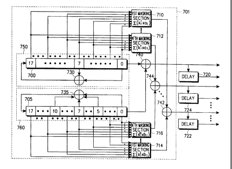
Referring to Fig. 7, the scrambling code group
generator 701 comprises a first m-sequence generator 750
including: an upper shift register memory (hereinafter,
referred to as "first shift register memory") 700 (with
registers 0 to 17) and an adder 730, a second m-sequence
generator 760 including; a lower shift register memory
(hereinafter, referred to as "second shift register
memory") 705 (with registers 0 to 17) and an adder 735, a
plurality of masking sections 710 to 712, 714 to 716, a
plurality of adders 742 to 744 and 740, and a plurality of
CA 02342808 2004-11-25
75998-164
-17-
delays 722 to 724 and 720. The first shift register memory
700 stores a predetermined register initial value "a0" and
the second shift register memory 705 stores a predetermined
register initial value "b0". The values stored in each of
the registers in the memory 700 and the memory 705 may
change during every period of an input clock (not shown).
The register memory 700 and 705 store 18 bit (or symbol)
binary values "ai" and "bi", respectively (i = 0 to c-1 where
c = the total number of registers in the register memories
700 and 705).
The first m-sequence generator 750 generates a
first m-sequece using the register memory 700 and the
adder 730 which is a binary adder that adds the binary
values from the registers 0 and 7 of the register memory 700
and outputs the sum into the register 17. The register 0 of
the register memory 700 sequentially outputs binary values
that form the first m-sequence during every period of the
input clock. The masking sections 710 to 712 store mask
code values (kli to kNi ) for generating cyclical shifts of
the first m-sequence by a predetermined number of chips.
The cyclical shifts are achieved by multiplying the mask
code values by the register value "ai" of the first shift
register memory 700, as expressed by the following equation:
(k`1 xa;) (L = 1 to N) . The resulting values are provided to
the adders 742 to 744, respectively.
The second m-sequence generator 760 generates a
second m-sequence using the register memory 705 and the
adder 735 which is binary adder that adds the binary values
from the registers 0, 5, 7 and 10 of the register memory 705
and outputs the sum into the register 17. The register 0 of
the register memory 705 sequentially outputs binary values
that form the second m-sequence during every period of the
CA 02342808 2004-11-25
75998-164
-18-
input clock. The masking sections 714 to 716 store each
mask code values (sli to s"i ) for generating cyclical shifts
of the second m-sequence by a predetermined number of chips.
The cyclical shifts are achieved by multiplying the mask
code values by the register value "bi" of the second shift
register memory 705. The resulting values are provided to
the adders 742 to 744, respectively. Each of the m-sequence
generators 750 and 760 generates an m-sequence according to
the corresponding generator polynomial.
The adder 740 adds the 0-th register values (i.e.,
the last bits) of the first and second shift register
memories 700 and 705 to generate a scrambling code, which
becomes the primary scrambling code. The adders 742 to 744
add one bit generated from each of the masking sections 710
to 712 connected to the first shift register memory 700 to
one bit generated from the masking sections 714 to 716
corresponding to the masking sections 710 to 712,
respectively. In other words, the output from the first
masking section 710 from the first group is added with the
output from the first masking section 714 from the second
group and so on, until the output from the Nth masking
section 712 from the first group is added with the output
from the Nth masking section 716 from the second group.
Thus, each of the masking sections 710 - 712 in the first
group has a corresponding masking section in the masking
sections 714 - 716 of the second group. The outputs from
the corresponding masking sections are added together in the
adders 742 - 744, respectively. That is, the individual
masking sections have a conjugate on a one-to-one basis with
respect to the first and second shift register memories 700
and 705. For example, the first masking section 710 of the
first shift register memory 700 corresponds to the first
masking section 714 of the second shift register memory 705,
CA 02342808 2004-11-25
75998-164
-19-
the N-th masking section 712 corresponding to the N-th
masking section 716, and so on. Between the two conjugate
masking sections (i.e., first masking sections 710 and 714,
or N-th masking sections 712 and 716) is connected the
adder 742 to 744 that add the two bits output from the
masking sections in response to the input clock. Here, the
output signals of the summers 742 to 744 have an I-channel
component.
The delay 722 to 724 and 720 delay the I-channel
signals for a predetermined number of chips to generate
respective Q-channel signals.
Now, a description will be given to an operation
of the present invention as constructed above.
Once an initial value for the primary scrambling
code is applied to the first and second shift register
memories 700 and 705 each having 18 registers for cyclically
shifting the register value "ai" or "bi", the 0-th register
values of the first and second shift register memories 700
and 705 are fed into the adder 740 and the 18 register
values "ai" of the first shift register memory 700 are fed
into the first to N-th masking sections 710 to 712 in order
to generate cyclically shifted sequences of the first shift
registers. Meanwhile, the 18 register values "bi" of the
second shift register memory 705 are fed into the first to
N-th masking sections 714 to 716 in order to generate
cyclically shifted sequences of the first shift registers.
Then, the first masking section 710 masks the input values
from the first (upper) shift register memory 700 (all 18
bits from 18 registers in the shift register memory 700)
with a mask function kli (i . e . , 1:(k' x a;)) and outputs the
masked values to the summer 744 for generating the first
secondary scrambling code. The masking is concurrently
CA 02342808 2004-11-25
75998-164
-20-
processing in every masking sections 710 - 712. The N-th
masking section 712 masks the input values from the first
(upper) shift registers with a mask function kNi (i.e.,
J(kN;xai)) and outputs the masked values to the summer 744
for generating the N-th secondary scrambling code. The N-th
masking section 716 masks the input values from the second
(lower) shift registers with a mask function 5Ni (i.e.,
Z(sN;xa;)) and outputs the masked values to the summer 742
for generating the N-th secondary scrambling code. The
first masking section 714 masks the input values from the
register memory 705 with a mask function sli (i.e., Z(s'; xa;) )
and outputs the resulting values to the adder 742 for
generating the first secondary scrambling code. Each of the
masking sections 710 - 712 masks the input values from the
first shift register memory 700 and outputs the masked value
to the respective adders 742 - 744. Then, the adder 740
adds the output bits from the 0-th registers of the first
and second shift register memories 700 and 705. These
generated output signals are immediately delayed at the
delay 720. The adder 744 adds the output bits from the N-th
masking sections 712 and 716 to generate I-channel signals,
which are immediately fed into the delay 724. The delay 722
delays the I-channel signals output from the adder 744 for a
predetermined number of chips to generate Q-channel
scrambling signals. The adder 742 adds the output bits from
the first masking sections 710 and 714 to generate I-channel
signals. These I-channel signals are immediately delayed
for a predetermined number of chips at the delay 722. Then,
the 0-th and seventh register values of the first shift
register memory 700 are added at the summer 730 and the
added value is inputted to the seventeenth register, as the
left-sided values are shifted to the right side by one and
the utmost left-sided register is newly filled with the
CA 02342808 2004-11-25
75998-164
-21-
output value of the summer 730. The 0-th, fifth, seventh,
and tenth register values of the second shift register
memory 705 are added at the adder 735, the added value is
inputted into the seventeenth register, as the left-sided
values are shifted to the right side by one and the utmost
left-sided register (i.e., the seventeenth register) with
the output value of the summer 735. This procedure is
repeated to generate multiple scrambling codes.
Fig. 8 is a diagram showing a scrambling code
generator of a receiver for concurrently generating one
primary scrambling code and one secondary scrambling code.
The receiver has only to use scrambling codes for a common
control channel and a data channel assigned thereto and thus
needs one primary scrambling code and one secondary
scrambling code.
Referring to Fig. 8, once an initial value for the
primary scrambling code is applied to a first shift register
memory 840 having 18 upper shift registers and a second
shift register memory 845 with 18 lower shifter register,
the 0-th register values of the first and second shift
register memories 840 and 845 are fed into an adder 810.
The output of the adder 810 is a primary scrambling code.
The 18 register values "ai" of the first shift register
memory 840 are fed into a masking section 820. Meanwhile,
the 18 register values "bi" of the second shift register
memory 845 are fed into a masking section 825. Then, the
masking section 820 masks the input values from the first
shift register with a mask function ki (i . e . , E(k; x a)) and
outputs the masked values to an adder 815 for generating the
first secondary scrambling code. The masking section 825
masks the input values from the second (lower) shift
register with a mask function si (i . e . , j:(s; x a;)) and outputs
CA 02342808 2004-11-25
75998-164
-22-
the masked values to a summer 815 for generating the
secondary scrambling code. Then, the adder 810 adds the
output bits from the 0-th registers of the first and second
shift register memories 800 and 805 to generate I-channel
primary scrambling code signals. These I-channel primary
scrambling code signals are immediately delayed for a
predetermined number of chips at a delay 830 to generate
Q-channel primary scrambling code signals. The adder 815
adds the output bits from the masking sections 820 and 825
to generate I-channel primary scrambling code signals, which
are immediately delayed at a delay 835. Then, the 0-th and
seventh register values of the first shift registers are
added at the adder 800, and the added value is output to the
seventeenth register, as the left-sided values are shifted
to the right side by one. The 0-th, fifth, seventh and tenth
register values of the second shift registers are added at
the adder 805, and the added value is output to seventeenth
register, as the left-sided values are shifted to the right
side by one. This procedure is repeated to generate
multiple scrambling codes.
The scrambling code generator of the first
embodiment needs plurality of distinct mask functions stored
in the masking sections in order to generate each secondary
scrambling code, i.e., it uses 2N mask functions to generate
N scrambling codes. Accordingly, the structure of primary
and secondary scrambling codes shown in Fig. 6 enables
implementation of the scrambling code generator of the
transceiver structure shown in Figs. 7 or 8, which further
includes only 2N mask functions with a quite little hardware
complexity to generate multiple scrambling codes.
CA 02342808 2004-11-25
75998-164
-23-
Second Embodiment
Fig. 9 is a diagram showing the structure of
primary and secondary scrambling codes in accordance with a
second embodiment of the present invention. While the first
embodiment masks both m-sequences ml (t) and m2(t) to generate
scrambling codes, the second embodiment involves cyclic
shift of the m-sequence m2(t) only other than ml(t) to
generate scrambling sequences. That is, this embodiment is
well expressed by Equation 1.
Referring to Fig. 9, when M secondary scrambling
codes correspond to one primary scrambling code, the first,
(M+2) -th, (2M+3) -th, ..., ((K-1) *M+K) -th, ..., and (511M+512) -th
gold codes are used as primary scrambling codes. The
secondary scrambling codes corresponding to the ((K-1)*M+K)-th
gold code used as the (K)-th primary scrambling code are
composed of M gold codes, i.e., ((K-1)*M+(K+l)),
((K-1)*M+(K+2))..., and (K*M+K)-th gold codes. Here, with 512
primary scrambling codes used, each of the secondary
scrambling code sets corresponding to the 512 primary
scrambling codes is composed of M secondary scrambling codes.
In this structure, if a cell uses one of the primary
scrambling codes then secondary scrambling codes belonging to
the secondary scrambling code group corresponding to the
primary scrambling code will be used when the secondary
scrambling codes need to be used. As shown in Fig. 9, once a
primary scrambling code is selected, the secondary scrambling
codes corresponding to the primary scrambling code are
generated by the adding cyclically shifted first m-sequences
and the second m-sequence. Here, the secondary scrambling
codes are generated through application of mask functions to
the sequences in the first shift register memory. This method
is adapted to a scrambling code generator of a transmitter as
illustrated in Fig. 10, which concurrently generates one
CA 02342808 2004-11-25
75998-164
-24-
primary scrambling code and multiple secondary scrambling
codes.
Referring to Fig. 10, the first m-sequence
generator 1050 comprises a first shift register memory 1040
(with registers 0 to 17) and an adder 1010 for adding the
outputs of the registers 0 and 7. The second m-sequence
generator 1060 comprises a second register memory 1045 (with
registers 0 to 17) and an adder 1015 for adding the outputs
of the registers 0, 5, 7 and 10. The scrambling code
generator shown in Fig. 10 comprises the two m-sequence
generators 1050 and 1060, a plurality of masking
sections 1000 to 1005, a plurality of adders 1032 to 1034
and 1030, and a plurality of delays 1022 to 1024 and 1020.
The first shift register memory 1040 stores a predetermined
register initial value "ao" and the second shift register
memory 1045 stores a predetermined register initial value
"bo". The shift register memory 1040 and 1045 can store 18
binary values (bits or symbols) "ai" and "bi" (0 _< i <_ 17
The two m-sequence generators 1050 and 1060 generate
respective serial output sequence bits according to each
generation polynomials at every period of the input clock
(not shown). The second embodiment of the present invention
uses a gold code length of 38400 symbols to generate
scrambling codes. Thus, the shift register memories 1040
and 1045 may be reset to the initial value when each of the
register memories 1040 and 1045 outputs a sequence having a
length of 38400 symbols.
The first m-sequence generator 1050 generates the
first m-sequence using the register memory 1040 and the
adder 1010 which is a binary adder that adds the binary
values from the registers 0 and 7 of the register
memory 1040 and outputs the sum into the register 17. The
register 0 of the register memory 1040 sequentially outputs
CA 02342808 2004-11-25
75998-164
-25-
binary values that form the first m-sequence during every
period of the input clock. The masking sections 1000 to 1005
store mask code values (kli to kNi) for generating cyclical
shifts of the first m-sequence by a predetermined number of
chips. The cyclical shifts are achieved by multiplying the
mask code values by the register value "ai" of the first
shift register memory 1040, as expressed in the following
equation: Y(K`';xa;). The resulting values are provided to
the adders 1032 to 1034, respectively. In the preferred
embodiments of the present invention, each of the mask code
values (kli to kNi) creates a new sequence which is a first
m-sequence cyclically shifted 1 to N times. Thus, each of
the mask code values is determined by the desired number of
cyclical shifting.
The adder 1030 adds the 0-th register values of
the first and second shift register memories 1040 and 1045
to generate a scrambling code, which becomes a primary
scrambling code. The adders 1032 to 1034 each adds one bit
generated from the masking sections 1000 to 1005 to one bit
generated from the second shift register memory 1045,
respectively, to generate I-channel scrambling code signals.
Here, the output from the adder 1030 is used as the primary
scrambling code and the scrambling codes output from the
adders 1032 to 1034 can be used as secondary scrambling
codes that corresponds to the primary scrambling code. The
following is an example of possible mask values (kli to k i)
kli =(000000000000000010), k2 = (0000 00000000000100), k3i
=(0000000000000001000).... By controlling the mask values,
other primary and secondary codes can be generated. The
following example shows how to obtain a necessary mask code
to cyclically shift a m-sequence `n' times. In general,
divide x by the generation polynomial for the m-sequence
(i.e., x" /f(x)) and take the remainder of the division to
CA 02342808 2004-11-25
75998-164
-26-
form the mask code. For example, if a mask code that
cyclically shifts 31 times is desired, take x31 and divide it
by f(x) =x18 +x' +1 the generation polynomial and find the
remainder which cannot be divided further. The final
remainder is x13 + x9 + x2 as shown by the following:
x31 =x13x18 =x13(x'+1)=x20+x13 =x2x18+x13 =x2(x7+1)+x13 =x13+x9+x2
The binary sequence corresponding to x' 3 + x9 + x2
is 000010001000000100 which is the mask code needed to
cyclically shift the m-sequence 31 times.
The delays 1022 to 1024 and 1020 delay the
I-channel signals for a predetermined number of chips to
generate Q-channel scrambling code signals.
As described above, the second embodiment of the
present invention generate scrambling code groups shown in
Fig. 9 and only uses one gold code generator, masking
sections 1000 to 1005 and adders 1022 to 1034.
Now, a description will be given to an operation
of the present invention as constructed above.
Once an initial value for the primary scrambling
code is applied to the first and second shift register
memories 1040 and 1045 each having 18 registers, the 0-th
register values of the first and second shift register
memories 1040 and 1045 are fed into the adder 1030 and the
18 register values "ai" of the first shift register memory
1040 are fed into the first to N-th masking sections 1000 to
1005 in order to generate 1 to N cyclically shifted
sequences of the first m-sequence. Then, the first masking
section 1000 masks the input value(ai) from the first (upper)
shift register memory 1040 with a mask function k1i for
generating the first secondary scrambling codes (i.e.,
CA 02342808 2004-11-25
75998-164
-27-
Y(k'; xa;)) and outputs the masked value (ai) to the adder
1032. The N-th masking section 1005 masks the input value(ai)
from the first (upper) shift register memory 1040 with a
mask function k N i for generating the N-th secondary
scrambling codes (i.e., J(kN;xa;)) and outputs the masked
values to the adder 1034. At the same time, the adder 1030
sums the output bits from the 0-th registers of the first
and second shift register memories 1040 and 1045. The
generated output signals are immediately delayed at the
delay 1022. The adder 1032 sums the output bits from the
first masking section 1000 and the 0-th shift register of
the second shift register memory 1045. The output signals
are immediately fed into the delay 1022. Thereafter, the
0-th and seventh register values of the shift register
memory 1040 are added at the adder 1010 and the adder 1010
outputs the sum to the seventeenth register, as the left-
sided values are shifted to the right side by one and the
utmost left-sided register is newly filled with the output
value of the adder 1010. The 0-th, fifth, seventh and tenth
register values of the shift register memory 1045 are added
at the adder 1015, and the adder inputs the sum into the
seventeenth register of the register memory 1045 as the
left-sided values are shifted to the right side by one to
fill the utmost left-sided register (i.e., the seventeenth
register) with the output value of the adder 1015. This
procedure is repeated to generate multiple scrambling codes.
Fig. 11 is a diagram showing a scrambling code
generator of a receiver for concurrently generating one
primary scrambling code and one secondary scrambling code.
The embodiments shown in Figs. 10 and 11 can be used either
in a transmitter or a receiver.
CA 02342808 2004-11-25
75998-164
-28-
The receiver according to the second embodiment of the
present invention has only to use one secondary scrambling
code and thus needs only one masking section 1100.
Referring to Fig. 11, once an initial value for
the primary scrambling code is applied to a first shift
register memory 1140 having 18 registers and a second shift
register memory 1145 with 18 registers, the 0-th register
values of the first and second shift register memories 1140
and 1145 are fed into an adder 1120. The 18 register values
"ai" of the first shift register memory 1140 are fed into the
masking section 1100 in order to generate a cyclically
shifted m-sequence. Then, the masking section 1100 masks
the input values(ai) from the register memory 1140 with a
mask values ki for generating the first secondary scrambling
codes (i.e., Y(k1xa;)) and outputs the masked values to an
adder 1125. The adder 1120 sums the output bits from the
0-th registers of the first and second shift register
memories 1140 and 1145. The output signals of the
adder 1120 are immediately delayed at a delay 1130.
Meanwhile, the adder 1125 sums the output bits from the
masking section 1100 and the 0-th shift register of the
second shift register memory 1145 and outputs the sum to a
delay 1135 immediately. Then, the 0-th and seventh register
values of the first shift register memory 1140 are added at
the adder 1110, in which case the left-sided values are
shifted to the right side by one and the utmost left-sided
register is newly filled with the output value of the
summer 1110. The 0-th, fifth, seventh and tenth register
values of the second shift register memory 1145 are added at
the adder 1115, shifting the left-sided values to the right
side by one and newly filling the utmost left-sided register
with the output value of the adder 1115. The mask values
CA 02342808 2004-11-25
75998-164
-29-
can be controlled by a controller (not shown) when the
receiver needs to generate other scrambling codes.
The scrambling code generator of the second
embodiment needs mask values stored in the masking section
in order to generate the secondary scrambling code, i.e., it
uses N mask values to generate N scrambling codes.
Accordingly, the structure of primary and secondary
scrambling codes shown in Fig. 9 enables implementation of
the scrambling code generator of the transceiver structure
shown in Figs. 10 and 11, which further includes only N mask
functions with a quite little hardware complexity to
generate multiple scrambling codes.
While the invention has been shown and described
with reference to a certain preferred embodiment thereof, it
will be understood by those skilled in the art that various
changes in form and details may be made therein without
departing from the spirit and scope of the invention as
defined by the appended claims.