Note: Descriptions are shown in the official language in which they were submitted.
CA 02342883 2001-03-02
WO 00/14910 PCT/US99/20102
Precision Timing Generator
System and Method
Background of the Invention
Field of the Invention
This invention generally relates to radio systems and, more specifically, to
a precision timing generator for impulse radio technologies, such as
communication systems, radar, and security systems.
Related Art
Recent advances in communications technology have enabled
communication systems to provide ultra-wideband communication systems.
Among the numerous benefits of ultra-wideband communication systems are
increased channelization, resistance to jamming and low probability of
detection.
The benefits of ultra-wideband systems have been demonstrated in part by
an emerging, revolutionary ultra-wideband technology called impulse radio
1 S communications systems (hereinafter called impulse radio). Impulse radio
was
first fully described in a series of patents, including U.S. Patent Nos.
4,641,317
(issued February 3,1987), 4,813,057 (issued March 14,1989), 4,979,186 (issued
December 18,1990), 5,363,108 {issued November 8,1994} and 4,743,906 (issued
May 10, 1988) all to Larry W. Fullerton. A second generation of impulse radio
patents includes U.S. Patent Nos. 5,677,927 (issued October 14,1997),
5,687,169
(issued November 1 l, 1997} and co-pending Application No. 08/761,602 (filed
December 6, 1996; now allowed) to Fullerton et al. These patent documents are
incorporated herein. by reference.
CA 02342883 2001-03-02
WO 00/14910 PCTNS99/20102
-2-
Basic impulse radio transmitters emit short Gaussian monocycle pulses
with tightly controlled pulse-to-pulse intervals. Impulse radio systems use
pulse
position modulation, which is a form of time modulation in which the value of
each instantaneous sample of a modulating signal is caused to modulate the
position of a pulse in time.
For impulse radio communications, the pulse-to-pulse interval is varied on
a pulse-by-pulse basis by two components: an information component and a
pseudo-random (PN) code component. Generally, spread spectrum systems make
use of PN codes to spread the information signal over a significantly wider
band
of frequencies. A spread spectrum receiver correlates these signals to
retrieve the
original information signal. Unlike spread spectrum systems, the PN code for
impulse radio communications is not necessary for energy spreading because the
monocycle pulses themselves have an inherently wide bandwidth. Instead, the
pseudo-random code of an impulse radio system is used for channelization,
energy
smoothing in the frequency domain, and jamming resistance (interference
rejection.)
Generally speaking, an impulse radio receiver is a homodyne receiver with
a cross correlator front end. The front end coherently converts an
electromagnetic
pulse train of monocycle pulses to a baseband signal in a single stage. The
data
rate of the impulse radio transmission is typically a fraction of the periodic
timing
signal used as a time base. Each data bit time position usually modulates many
of
the transmitted pulses. This yields a modulated, coded timing signal that
comprises a train of identically shaped pulses for each single data bit. The
cross
correlator of the impulse radio receiver integrates multiple pulses to recover
the
transmitted information.
In an impulse radio communication system, information is typically
modulated by pulse-position modulation. That is, the time at which each pulse
is
transmitted is varied slightly from the predetermined pulse-to-pulse interval
time.
One factor limiting the effectiveness of the communication channel is the
accuracy
with which the pulses can be positioned. More accurate positioning of pulses
can
CA 02342883 2001-03-02
WO 00/14910 PCT/US99/20102
-3-
allow the communication engineer to achieve enhanced utilization of the
communication channel.
For radar position determination and motion sensors, including impulse
radio radar systems, precise pulse positioning is crucial to achieving high
accuracy
S and resolution. Limitations in resolution of existing systems are partially
a result
ofthe limitations in the ability to encode a transmitted signal with a
precisely timed
sequence. Therefore, enhancements to the precision with which timing signals
can
be produced can result in a higher-resolution position and motion sensing
system.
Impulse radio communications and radar are but two examples of
technologies that would benefit from a precise timing generator. A high-
precision
timing generator would also find application in any system where precise
positioning of a timing signal is required.
Generating such high precision pulses, however, is quite difficult. In
general, high precision time bases are needed to create pulses of short
duration
having tightly controlled pulse-to-pulse intervals. Currently available analog
or
digital integrated circuit timers are not capable of creating such high
precision
pulses. Typical impulse radio timer systems are relatively complex, expensive,
board level devices that are difficult to produce. A small, low power, easily
produced, timer device would enable many new impulse radio-based products and
bring their advantages to the end users.
Summary of the Invention
The present invention relates to a timing generator that provides highly
accurate, stable, low fitter, and agile timing signals in response to a
rapidly
changing timing command input. Such signals are needed for UWB transceiver
and radar devices as well as numerous other applications in industry and
instrumentation.
Timing signals generated in accordance with this invention result in a signal
transition at a precisely spaced (delayed) time relative to a time framing
signal also
CA 02342883 2001-03-02
WO 00/14910 PCT/US99/20102
-4-
generated by the system. The framing signal is typically slaved to a stable
reference. In one embodiment, a phase locked loop (PLL) is used to accomplish
this function. If the timing command meets certain setup time requirements,
the
output timing signal transition will be placed at a precise time relative to
the -
associated frame signal transition. An early/late command input signal and
associated mechanism are included to permit 100% time command caverage-free
of gaps caused by setup time or metastable restrictions.
The invention utilizes a coarse timing generator and a fme timing generator
to accomplish this goal. The coarse timing generator is utilized to define the
framing interval and to further subdivide the framing interval into coarse
timing
intervals. The fine timing generator is used to define the time position
between
coarse timing intervals.
The coarse timing generator utilizes a high-speed synchronous counter, an
input command latch and a digital comparator. One embodiment permits latching
the input command at several points to permit 100% timing coverage. Another
embodiment includes selectable counter lengths to scale the system to
different
frame rates and different reference timer frequencies. These setup parameters
can
be loaded using a serially loadable command register.
The fine delay generator is based on a phase shift circuit. Two example
embodiments are described. One is based on a sine/cosine multiplier phase
shift
circuit; the other is based on an RLC switched element phase shift circuit.
The
sine/cosine multiplier circuit utilizes a sine wave version of the coarse
delay clock
together with analog voltages representing the sine and cosine ofthe desired
phase
shift angle to produce a sine wave timing signal shifted in time (phase)
fractionally
between two coarse delay intervals. In one embodiment, the fine timing
generator
uses an analog command input and as a result has a continuous rather than
quantized transfer function. In another embodiment. the fine timing input is
digital
and is mapped through a memory device that drives a digital-to-analog
converter
(DAC) to produce the correct timing associated with the digital input command.
This signal is combined with the coarse delay signal to produce the output
delay
CA 02342883 2001-03-02
WO 00/14910 PCTNS99/20102
-S-
signal, which is the sum of the two delays. In one embodiment, the delay
generator contains two sets of sine/cosine generators to permit 100% timing
coverage.
A unique advantage of the combiner circuit is that the coarse delay signal --
S may have errors much larger than the final timing requirement. The coarse
delay
signal is only used to select among several fine delay signals. The fine delay
signals determine the precision of the output.
An alternate embodiment of the phase shifter utilizes switched lumped
element phase networks. This arrangement takes a direct digital input and does
not need a DAC or a sine/cosine lookup table.
One embodiment of this invention implements the coarse and fine delay
sections in a Site ASIC (chip) and partitions the system such that random
access
memories (RAM's) and digital-to-analog converters (DAC's) are external to the
ASIC. In this embodiment, further advantages result from implementing the
1 S circuitry in fully differential current steering logic and differential
analog amplifiers
such that the chip draws a constant current independent of clock frequency.
This
minimizes on-chip transients that could introduce fitter in the output.
One of the unique challenges of UWB transceivers is that they not only
need stable and accurately timed pulses, typically to 30 picoseconds (ps) and
stable over millisecond (ms) correlation intervals, but the timing needs to
change
dramatically from pulse to pulse. This interval may be on the order of 100
nanoseconds (ns) and needs to be accurate to fractional parts per thousand
relative
to an implementation-specific standard 1 OOns frame interval. This invention
has
demonstrated the ability to meet these timing requirements and when
implemented
2S in ASIC form, it enables the production of relatively economical UWB
systems.
For simplification, the invention is described by referring to diagrams that
are single ended, but the preferred implementation is to use differential
circuits.
Various input and output signals are shown as differential.
An advantage of the invention is that timing pulses can be precisely
positioned in time to a high degree of accuracy. As a result, advancements in
CA 02342883 2001-03-02
WO 00/14910 PCT/US99/20102
-6-
communication technology can be realized. For example, in a communication
system utilizing pulse position modulation, gains can be achieved in coding
and
bandwidth by taking advantage of the ability to more precisely position the
timing
of the pulses in the nominal period. '
Additionally, because precise positioning can be achieved over the entire
nominal period, the entire period can be utilized for communication, thereby
resulting in increased channelization of the communication system.
Advantages are also realized in radar and motion sensor applications.
More precise positioning of output pulses allows a higher resolution radar and
motion sensor system.
Further features and advantages of the present invention, as well as the
structure and operation of various embodiments of the present invention, are
described in detail below with reference to the accompanying figures.
CA 02342883 2001-03-02
WO 00/14910 PC'T/US99/20102
Brief Description of the Figures
The present invention is described with reference to the accompanying
figures. In the figures, like reference numbers indicate identical or
functionally
similar elements. Additionally, the left-most digits) of a reference number
identifies the figure in which the reference number first appears.
FIG's. 1 A and 1 B are block diagrams of an impulse radio transmitter and
receiver, respectively, which comprise an example communication system that
uses the present invention;
FIG's. 2A and 2B illustrate an unmodulated pulse train and a nominal
periodic occurrence of a pulse, respectively;
FIG. 3 is a block diagram of an example impulse radar sensor, which uses
the present invention;
FIG. 4 illustrates a block diagram of a precision timing generator in
accordance with the present invention;
FIG. 5 is a more detailed diagram if the fine delay block of FIG. 4;
FIG. 6 is a flow diagram of the steps in FIG. 4;
FIG. 7 illustrating an example implementation of a precision timing
generator in accordance with an embodiment of the present invention;
FIG. 8 illustrates a block diagram of a precision timing generator
implemented using an ASIC, in accordance with the present invention;
FIG. 9 illustrates a coarse timing generator in accordance with an
embodiment of the present invention;
FIG. 10 illustrates latch enable timing in accordance with an embodiment
of the present invention;
FIG. 11 illustrates latch enable, early/late and A/B system timing in
accordance with an embodiment of the present invention;
FIG. 12 illustrates a combiner circuit in accordance with an embodiment
of the present invention;
CA 02342883 2001-03-02
WO 00/14910 PCT/US99/20102
_g_
FIG.13 is a fine timing generator in accordance with an embodiment ofthe
present invention;
FIG. 14 illustrates an exemplary ploy-phase filter that can be used for the
phase locked loop for FIG. I3;
FIG. 1 S is a timing diagram illustrating the basic operation of the combiner
circuit of FIG. 12;
FIG. 16 is a timing diagram illustrating the details of the early/late signal
in accordance with an embodiment of the present invention;
FIG. 17 is a timing diagram illustrating further details of the early/late
signal;
FIG. 18 illustrates an alternate fine timing generator in accordance with
another embodiment of the present invention;
FIG's. 19 and 20 illustrate a further alternate fine timing generator in
accordance with another embodiment of the present invention;
1 S FIG's. 21 A, 21 B, and 21 C illustrate code mapping and timing
considerations in a system designed without the E/L function in accordance
with
another embodiment of the present invention;
FIG. 22 illustrates an example Site differential AND gate for the ASIC
in accordance with another embodiment of the present invention.
CA 02342883 2001-03-02
WO 00/14910 PCT/US99/20102
-9-
Detailed Description of the Preferred Embodiments
1. Overview and Discussion of tl:e Invention
The present invention is directed to a system and method for generating
highly agile and precise timing signals as are typically required for impulse
radio
systems. According to the invention, a coarse timing generator is utilized to
generate a coarse timing signal at a coarse time interval within a nominal
frame
interval. A fine timing generator, synchronized to the coarse timing
generator,
provides a set of fine time intervals that interpolate between coarse time
intervals.
A combining circuit utilizes the coarse timing signal to select the correct
fme
timing signal that drives the output. This system is typically phase locked to
a
stable reference oscillator source, which provides good long term drift
performance. In an exemplary application, this system is capable of providing
timing for near 1 Ops positioning of sub-nanosecond pulses with in a I OOns
frame
with less than Sons setup time. This timing is needed for pseudo random code
positioning of pulses in impulse radio communications and radar equipment, and
the like.
2. Significance of tl:e Invention
Before describing the invention in detail, it is useful to describe two
example scenarios in which the invention finds utility. These scenarios are
provided as an example only and as an aid in understanding potential
applications
of the invention. It is not intended that the invention be limited to
application in
these scenarios. In fact, in a broad sense, the invention can he implemented
in any
system requiring or desiring a precision timing signal or a precision time
delay
means. Thus, the invention i s well suited to high-speed computer applications
and
ultra-wideband communications systems. The precision provided by the time
generator according to the invention is especially beneficial to impulse radar
and
CA 02342883 2001-03-02
WO 00/14910 PCT/US99/20102
-10-
communication systems., although, as indicated above, its application is not
limited
to such systems.
FIG. 1 is a simplified block diagram illustrating an example of an ultra-
wideband (e.g., impulse radio) communication system. Referring now to FIG.1 A,
the impulse radio communication system includes a transmitter 104 (which could
be a stand-alone transmitter, or the transmit portion of a transceiver), and a
receiver FIG. 1 B 108 (which could be a stand-alone receiver, or the receive
portion of a transceiver).
Without modulation, transmitter 104 transmits a periodic series of pulses
spaced at a predefined time interval. Data is modulated onto this series by
altering
the time at which the pulses are positioned. This can be referred to as pulse-
position modulation. FIG. 2A is a diagram illustrating an unmodulated pulse
train.
In the example illustrated in FIG. 2A, pulses are transmitted at periodic
intervals
indicated by the reference character TF. For example, for an unmodulated pulse
train, each pulse can be timed to occur every 100 ns, although other periods
may
be chosen. In this document, the period is referred to as a frame. Thus, each
frame is 100ns long.
Pulses, however. are not usually transmitted at regular frame intervals
because this gives rise to a comb line spectrum where each line contains too
much
concentrated spectral power. To avoid this, the pulses are transmitted at
random
or pseudo-random intervals within the frame to "randomize" the pulse position
and spread the comb lines to smooth the spectrum. To maintain synchronization
between a transmitter and receiver, these pulses must be positioned to within
1 /10
wave at the center frequency of the pulse and for best performance, the pulse
should be agile enough to be placed anywhere within the frame. In addition,
frame
to frame positioning should have minimum correlation. The present invention
relates to a timing system that can provide this timing.
In a communications system, it is also necessary to add modulation to the
signal. This can be done with AM, FM, pulse position modulation, and other
methods described in the referenced patents. Typically pulse position
modulation
CA 02342883 2001-03-02
WO 00/14910 PCT/US99/20102
-11-
is chosen for its simplicity and efficiency. An example is shown in FIG 2B.
Referring to FIG. 2B, TO is the nominal pulse position defined by the code
offset
as described above. T1 is a pulse position with an additional offset due to
modulation. A typical system may transmit a pulse at position TO for data = 0
and
at T1 for data =1. For this system to work, the timing generator must be
capable
of providing timing to much greater precision than the modulation time shift
in
order to maintain good signal to noise.
Additional benefits can be obtained by using more than one pulse to
represent one digital information bit. The received signal from the ensemble
of
pulses associated with each bit is combined in a process referred to as
integration
gain. The combination process is basically the summation of the received
signal
plus noise energy associated with each pulse over the number of pulses for
each
bit. The voltage signal-to-noise ratio improves roughly by the square root of
the
number of pulses summed. Proper summation requires that the timing be stable
and accurate over the entire integration (summation) time.
Referring again to FIG. 1 A, time base 108 drives the precision timing
generator 120 and ensures long term stable operation. A code generator 112
provides a new time offset command for each new time frame. A time framing
clock (also referred to as a reference clock) is provided to the code
generator from
the timing generator. Data is supplied to the precision timing generator 120,
which modulates the timing in accordance with the data. The timing output
signal
is supplied to a pulser 124, which generates the RF pulse to be transmitted by
an
antenna 128.
FIG. 1B is a block diagram of an example impulse radio receiver.
Referring to FIG. 1 B, the time base 108 (same or duplicate of 108 in the
receiver
104) drives the precision timing generator 120 which provides long term
stability,
much as in the transmitter FIG. 1 A described above. except in this case, the
time
base 108 must be locked to the transmitter in periodicity and time offset. The
code generator 112 provides time offset commands identical to the code set
driving the transmitter. The resulting timing signals drive a template
generator
CA 02342883 2001-03-02
WO 00/14910 PCT/US99/20102
-12-
132 that produces a correlation template signal that matches the shape of the
signal received by the antenna 128. (Note that correlation includes sampling
and
implies signal integration over the aperture time of a correlator/sampler
136.) The
correlation signals from the ensemble of pulses comprising one data bit are
summed in a summing accumulator 140. The output of the accumulator 140 is
typically sampled at the end of the integration cycle by a detector (e.g.,
comparator) 144 to determine if the data bit is a one or a zero. The
correlation
signal also feeds a tracking loop filter l 48, which keeps the receiver time
base 108
in lock step with the received signal. Additional detail and variations may be
found in the referenced patents.
Consider now an impulse radar position or motion sensor application.
FIG. 3 is a simplified block diagram illustrating an ultra-wideband radar
sensor.
The impulse radar sensor operates by transmitting a pulse toward a target and
receiving the reflected pulse by the receiver at a delayed time determined by
the
offset time. This offset time determines an equivalent range of sensitivity
that is
referred to as the range gate. A typical impulse radar sums the return signal
from
a large number of pulses to improve signal to noise and thus the operating
range
achievable for a given pulse energy.
Referring to FIG. 3, the time base 108 drives the precision timing
generator 120 with a stable clock. The code generator 102 supplies pseudo-
random time offsets that are used to spread the comb spectrum of the
transmitted
pulses and provide for simultaneous operation of multiple radars. Multiple
radars
may be operated in the same area by setting each one to operate using
different
codes or different pulse frequencies. Other methods are disclosed in the
referenced patents. The precision timing generator 120 delivers a timing pulse
to
the pulser 124 according to the code generator input. The pulser 124 delivers
an
RF pulse 302 to the antenna 128, which is directed to a target 304 and a
reflected
pulse 306 is received by the receiving antenna 128 and fed to the correlator
136.
The correlator 136 is also fed a template signal (from template generator
132),
which is delayed a specific amount from the time of the transmitted pulse.
This
CA 02342883 2001-03-02
WO 00/14910 PCT/US99/20102
-13-
delay is provided to the template generator 132 by a time offset block 152.
The
result of the correlation of the received signal with the template signal is
fed to the
pulse summation accumulator 140. The result of multiple pulses is fed to the
processing circuitry (or computer) 160 where the signal is processed and
detected.
In some cases the signal is simply displayed, in other cases the signal is
subtracted
from a stored memory of the long term history to detect motion or changes.
Further details as well as architecture and algorithm variations may be found
in the
referenced patents.
Thus, the impulse radio system and impulse radar system are examples of
two systems that would benefit from a high-precision time base according to
the
present invention. The reader is again reminded that the application of the
precision time base disclosed herein is not limited to these two example
systems,
and, in fact, is not limited to application in ultra-wideband systems. After
reading
the description provided herein, it will become apparent to a person skilled
in the
1 S relevant art how to implement the invention in alternative systems and
environments.
3. TJ:e Present Inver:tion
FIG. 4 is a block diagram illustrating a precision timing generator 400
according to the present invention. Precision timing generator 400 corresponds
to block 120 of the earlier described f gures. Turning now to FIG. 4, the
timing
generator 400 includes a coarse timing generator 404, a fine timing generator
408,
and a combiner 412. A system clock signal 416 and a timing command input 420
drive the coarse and fine timing generators. Depending on the embodiment, the
system clock 416 can be self contained as part of the timing generator 400, or
it
can be an external input. The system clock 416 generates a CLK signal at a
first
frequency. The timing command input 420 is a data word specifying a desired
delay value, as will be discussed at length below. The coarse timing generator
404
generates a frame reference signal 432 and a coarse timing signal 428. The
coarse
CA 02342883 2001-03-02
WO 00/14910 PCTNS99/20102
-14-
timing signal 428 subdivides intervals of the frame reference signal 432 into
relatively coarse time intervals. The fine timing generator 408 generates a
fine
timing signal 429 that subdivides the coarse timing interval into smaller
intervals,
or in one embodiment, a continuously variable interval. The fine timing
generator --
408 generally produces several time transitions resulting in ambiguity at the
coarse
time interval. The combiner circuit 412 selects the fine timing signal 429
associated with the coarse timing signal 728 so as to resolve this ambiguity
and
produce a precision timing output 436.
FIG. 5 is an block diagram of the fine timing generator 408. The clock
signal 416 is used to generate a sine wave signal of the same frequency via a
sine
generator 504. The sine wave is typically created by a filter that strips the
harmonics from the square wave digital signal. The sine wave version of the
clock
is then fed to a phase shifter 508. The phase shifter 508 shifts the phase of
the sine
wave according to a fine time component of the timing command input 420. A
1 S block 512 labled "digital" converts the phase shifted sine wave into a
square wave
signal, which is forwarded to combiner 412.
In one embodiment, fine time component timing command input 420
comprises two analog DC level signals (static for the duration of a given
phase
shift value, but changed for a new phase shift value) representing the sine
and
cosine of the desired phase shift. In another embodiment the timing command is
a set of digital lines representing a set of discrete delay values to be
additively
combined. These two examples are described in greater detail in the discussion
of FIG's. 13 and 18. Alternative phase shift circuits are possible, as would
be
apparent to a person of ordinary skill in the art, without detracting from the
advantages of either the broader or specific features of the present
invention.
FIG. 6 is a flow diagram illustrating the operation of the timing generator
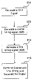
400. Referring now to both FIG's. 4 and 5, in a step 604, the system clock 416
generates CLK signal at a first frequency. In a step 608, the coarse timing
generator 404 generates a coarse timing signal 428. This coarse timing signal
428
CA 02342883 2001-03-02
WO 00/14910 PCT/US99/20I02
-15-
is a signal relative to the frame reference signal 432 and is a function ofthe
timing
command input 420.
In a step 612, the fine timing generator 408 generates a series of fine
timing signal transitions placed in time relative to the framing signal
according to --
the timing command input 420.
In step 616, the combiner 412 selects one of the fine timing signal
transitions according to the coarse timing signal 428 and outputs the
resulting
timing signal 436.
FIG. 7 is a block diagram illustrating an example implementation for the
precision timing generator 400. The timing generator 400 includes the system
clock 416 (shown as a voltage controlled oscillator or VCO) that produces the
CLK signal, a synchronous counter 704, a reference signal generator 708 (also
referred to as a reference clock or REF CLK), a phaselfrequency detector 712,
a
phase locked loop (PLL) filter 716, a comparator 720, a delay word latch 728.
The fine timing generator 408 and combiner 412 are shown as a single block for
simplicity.
In a preferred embodiment, the counter 704 is a synchronous counter that
divides the CLK signal generated by system clock 416 into a lower-rate signal,
which is the frame reference signal 432. Also, in a preferred embodiment, the
comparator 720 is an eight bit comparator and the (delay word) latch 728 is an
eight bit latch. The frame reference signal 432 defines an interval of time,
so it is
also referred to as a "frame interval." The frame interval is defined by the
period
of the most significant bit of the counter 704.
The counter 704 also outputs a count value 764. The count value 764
defines the coarse time interval. More specifically. the count value 764
indicates
the number of periods 436 that have occurred in the current frame. In other
words, the count value 764 indicates the amount of time elapsed since the
beginning of the current frame.
In order to enable a user to select the timing of the coarse timing signal
428 (i.e., the timing of the occurrence of the coarse delay pulse in the
preferred
CA 02342883 2001-03-02
WO 00/14910 PCT/US99/20102
-16-
embodiment), the illustrated embodiment utilizes the comparator 720 and the
latch
728. A count value 764 corresponding to a desired coarse time interval is
loaded
into the latch 728, as represented in the figure as coarse delay word DCO-DC7.
The comparator 720 compares the value of DCO-DC7 latched in the latch 728 --
S with the value in counter 704, as counter 704 counts pulses of VCO 416. When
the value in the counter 704 matches the value in the latch 728, the coarse
timing
signal 428 changes state. In a preferred embodiment, the comparator 720 simply
outputs the coarse timing signal 428 in the form of a coarse timing pulse.
The coarse timing signal 428 is used to enable the fine timing generator
408 to trigger at the next interval. The combiner 412 then produces the timing
output 436.
One difficulty in implementing a high-precision timing generator is the
availability of a stable and accurate frequency source at high frequencies.
One
especially troublesome characteristic of high frequency signal generators is
the
tendency to drift over time. However, for high speed, high resolution or wide
bandwidth systems, high frequencies are often required.
In the present invention, the timing generator 400 utilizes a phase locked
loop (PLL) to maintain the stability of the VCO 416. In the embodiment
illustrated in FIG. 7, the PLL comprises the phase/frequency detector 712
(simply
referred to as the phase detector), the REF CLK 708 and the PLL filter 716.
Accuracy and stability are provided by phase locking the VCO 416 to a very
precise REF CLK 708. At frequencies such as, for example, 10 MHZ, extremely
stable and accurate reference signal generators are commercially available
(e.g.,
a crystal oscillator).
The phase detector 712 compares and synchronizes the output of the
synchronous counter (frame reference signal 432) with a reference signal 766
generated by the REF CLK 708. Because the frame signal 432 is divided down
from the pulse repetition frequency (i.e., 416's CLK signal), the phase
detector
712, and hence the REF CLK 708 operate at this much lower frequency. The
phase detector 712 outputs an error signal, which is received by the PLL
filter
CA 02342883 2001-03-02
WO 00/14910 PCT/US99/20102
-17-
716. The PLL filter 716 adjusts the VCO 416 so that the VCO is synchronized
to the REF CLK 708. In a preferred embodiment, the phase detector is a
phase/frequency type of detector known to those skilled in the art (e.g.,
Motorola
MC 14046). This detector allows a wide lock-in range and ensures a
deterministic --
lock-in of the VCO.
To further clarify the operation of the precision timing generator 400,
consider the following example. In a system with a 100ns frame interval, the
inventors desire to produce a timing signal delayed 56ns after the 100ns frame
signal. The 100ns frame interval is divided into 256 coarse delay intervals of
390.6ps each. The coarse delay value would then be the integer part of (56*
100/256), which is 21. The fme delay value would be the remainder, which is
0.875. The fine delay value would be used to select 0.875 of a cycle at the
coarse
delay rate. Thus, an "In0" value from a sine lookup table (described below)
would
be In0=sin(2*pi*0.875) _ -0.707 and an "In90" value from a cosine table would
be In90= cos(2*pi*0.875) = 0.707. Typically these values are read from a
sin/cos
lookup table and applied to a digital-to-analog (DAC; described in detail
below),
whereupon the resulting analog voltage is applied to the In0 and In90 inputs
of the
time delay system (also to be described in detail below}. If there is a fixed
time
delay offset between the coarse delay system and the fme delay system, this
can
be accounted for by adding a phase angle correction factor to the above
equations.
FIG. 8 is a diagram of one embodiment in which a portion of the timing
circuitry is implemented using an ASIC chip 802. Fig 8 illustrates how the
system
can be partitioned for optimum match with ASIC and component technology. In
this diagram the coarse delay 404, fine delay 408 and combiner 412 functions
are
on the Site chip 802 and DAC, RAM and VCO functions are off chip. This
allows maximum use of conventional technology for DAC's and RAM's, while
focusing the power of the Site process on the timing functions. This has the
added advantage of separating RAM and DAC transients from the sensitive timing
of ASIC 802. In keeping with this architecture the VCO 416's input, and timing
and frame clock outputs are differential signals to help reduce common mode
CA 02342883 2001-03-02
WO 00/14910 PCT/US99/20102
_18_
noise coupling, which can influence fitter. These signals are not shown as
differential in this figure for simplicity.
Additional advantages can be obtained by implementing the ASIC circuits
in differential form. The logic is implemented in fully differential current
steering
logic and the analog circuits include differential amplifiers and filters such
that the
chip draws a constant current independent of clock frequency. This minimizes
on-
chip transients that could introduce fitter in the output. These circuits will
be
apparent to one skilled in the art, and indeed example circuits that can be
adapted
to Site are substantially available in several cell libraries. However, for
completeness, as example Site differential AND gate is described below in
connection with FIG. 22.
Referring now to FIG. 8, a 16 bit delay value 808 is input to the timing
system 800 for each cycle of frame reference output 432 in which a timing
signal
is desired. The delay value 808 is stored in a register 876. The most
significant
bits (MSB's) are provided directly to a coarse delay latch (described below as
936) in the ASIC 802. The MSB's comprise a coarse delay word 840 (DCO-
DC7) 824. The least significant bits (LSB's) comprise a fine delay word (DFO-
DF7), and are converted to analog levels via an IQ RAM's 872,871 and DAC's
843,845. An E/L signal 841 is the specific MSB of DFO-DF7.
An ASIC serial bus 804 is a 3 wire input with Data In (DIN), shift Clock
(SCLK), and Chip Select (CS) signals. The serial bus 804 is made to operate in
a slave mode, with SCLK is provided to the ASIC module 802 from an external
source. When the chip select pin goes high data is clocked into an internal
shift
register via the DIN pin. as will be described below in connection with FIG.
9.
The ASIC 802 has four pins associated with an external 2.56GHz clock
(VCO 416). Typically a 20MHz to 40 MHZ reference clock708 is provided to the
ASIC on the VIN pin (shown at 812) and the 2.56GHz VCO 416 is provided via
differential pins (shown generally at 816). These clock signals are passed to
a
frequency/phase comparator inside the ASIC 802, which generates a VCO
correction signal 820 on a PFDOut pin. This PFDOut signal is fed back to the
CA 02342883 2001-03-02
WO 00/14910 PCT/US99/20102
-19-
VCO 416 to keep it and the frame reference output 432 phase locked to the
reference clock 708.
A blanking signal 828 is an active low signal that disables the output of the
ASIC 802, inhibiting timing pulses from being generated. --
There are two modes that the ASIC uses to latch coarse data words and
control signals selected by shifting a value of one into the FE bit of the
configuration shift register 920 (see FIG. 9, below). When the ASIC 802 is in
FE
mode it latches at the beginning of every frame. In this mode, an LE (Latch
Enable) signal 832 must remain low at all times. When the ASIC is not in FE
mode, LE 832 is used as an externally provided latch enable.
An A/B input 836 is used to select which internal fine delay circuits will
be used to delay the coarse pulse inside the ASIC. The primary purpose of this
is to allow less expensive and slower support components to be used. As an
example, while the A-DAC's 843 are settling the B-DAC's 848 are in use and
vise-versa. Since only one pair of DAC's needs to be stable at one time, each
set
of DAC's only need to run at half the speed of what a single non 'ping ponged'
set
of DAC's would need to run. The only inputs affected by the A/B circuitry are
the
InOA, In90A, InOB, and In90B lines.
The A/B signal 836 is produced by a flipflop 854. The frame reference
output signal 432 is applied to a clock input of flipflop 855 and the Q output
is
fed to the flipflop input. The Q output is provided to the ASIC and the A
channel
IQ RAM 872. Because the A and B channels function in a ping pong fashion, the
Q output is provided to an inverter 856, which is used to drive the B channel
IQ
RAM 871.
The fine timing channels A and B introduce propagation delays causing the
fine timing signals InOA. In90A, InOB, and In90B to lag the coarse delay word
DCO-DC7. This delay is compensated by delaying DCO-DC7 and the E/L signal
841 via a pair of pipeline delays 860 and 858. 'thus, the coarse and fine time
CA 02342883 2001-03-02
WO 00/14910 PCT/US99/20102
-20-
values are synchronized using the frame reference output signal 432 as a clock
input to flipflop 855 and pipeline delays 860 and 858.
Some economy can be obtained by not using the A/B function. In this
case, the A/B signal 836 is tied high or low by designer's choice and only one
corresponding set of DAC's is necessary, and pipeline delay blocks 858 and 860
can be eliminated. The impact on the system performance is that successive
code
positions cannot be closer than the DAC setup time. Although all code
positions
can still be reached in the LE latch mode, this configuration is typically
used in a
simplified system in which 50% of the code space is given up for setup time.
In
such a system, the delay word is latched on the rising edge of the FE signal
and
the first 50% of the frame (50ns for a IOOns frame) is not used. Codes are not
generated for this region.
The MSB's from register 876 comprise the coarse delay word 724, which
provides the ASIC 802 with an 8 bit parallel coarse delay value. This value
selects
a coarse delay window to be combined with a fme delay value produced by fme
delay circuits inside the ASIC, as describe below. A pipeline delay 860 is
provided
to synchronize the loading of the coarse delay word 724 with the frame
reference
output 432, in a manner that would be apparent to a person skilled in the
relevant
art is view of the discussions herein.
There are five analog inputs to the fine delay circuits of ASIC 802. InOA
and In90A are the IQ (sine, cosine) inputs to the A fine delay circuit, and
InOB and
In90B are the IQ inputs to the B fine delay circuit. The InRef 868 is an
analog
signal that gives a reference voltage to the IQ inputs. InRef should be set in
the
middle of the other analog input ranges. For example, if In0 and In90 go
between
1 and 4 volts, InRef should be set for 2.5 volts.
An E1L (early/late) signal 841 is provided to select which internal coarse
delay pulse the fine delay circuit will use as a reference. Inside the ASIC
chip 802,
as described below, the coarse delay pulse is run through a flipflop that
creates a
version of the signal that is delayed by a half clock cycle. The original
coarse
delay pulse is known as the early pulse and the delayed version is known as
the
CA 02342883 2001-03-02
WO 00/14910 PCT/US99/20i02
-21-
late pulse. The E/L signal tells the fine delay circuit which coarse pulse to
reference for creation of the final output delay. The timing of this signal is
dependent on the configuration of the IQ RAM 872. Without the E/L circuitry
the
ASIC would not be able to cover a full 100% coding span because there is no -'
single coarse delay pulse that is available over the entire fine delay span.
The E/L
signal allows for the selection of an alternate coarse delay pulse to fill in
the areas
that the original coarse delay pulse cannot cover.
In the implementation shown in FIG. 8, the digital values for the fine delay
are the lower 8 bits of register 876. These digital values are used to look up
a sine
and cosine value in the IQ RAM's 872,871 and are then converted to analogue
values by the DAC's 843 and 845. These analogue values are used by the ASIC
802 to generate the fine delay, as discussed in further detail below.
In an example setup, the blank signal 828 will be tied high so that the
ASIC outputs are enabled. The A/B line 836 will either be high, low, or
toggling
with each frame depending on which analog inputs are being used. The LE line
832 will be tied low and the serial bus will be used to select FE mode. This
sets
the ASIC to internally latch on every clock. A 16 bit digital delay word 876
will
be used to set up the ASIC for creating the delay. The most significant 8 bits
of
the delay word 876 will be directly used as an 8 bit coarse word 844 to be
applied
to the ASIC coarse word input. The least significant 8 bits will contain an
address
that will be sent to the IQ RAM's 872. The data coming out of the I and Q
RAM's for the specified address will be applied to two different DAC's. One
DAC for the 0 degree signal and one DAC for the 90 degree signal. When the IQ
RAM's are loaded with the shifted data table (see IQ RAM section) the most
significant bit of the fine delay word will be routed to the E/L input 841 of
the
ASIC. The ASIC will then create a pulse at the timing output 436 delayed to
match whatever value is supplied by the 16 bit delay word 808.
The present invention is preferably implemented with two fine delay
systems/circuits, A and B . Having two fine delay circuits allows one circuit
to be
CA 02342883 2001-03-02
WO 00/14910 PCT/US99/20102
-22-
set-up while the other is being used. This allows for the use of lower cost
components, while maintaining the same performance.
FIG. 9 illustrates the coarse timing generator 404 in greater detail in
accordance with a preferred embodiment of the present invention. This --
embodiment contains features for adapting the operation of the timing
generator
for different clock rates and different modes. Referring now to FIG. 9, a
configuration shift register 920 is used to set various internal states. Two
inputs
labeled DIN and SCLK, supply the configuration data and associated clock for
storing the data in the register, respectively, when enabled by the CS (chip
select).
Two bits, labeled SS and S6, are configuration bits that control the modulo
size
and associated divide ratio of the coarse delay system, respectively. The DO
and
D1 configuration bits control the divide ratio applied to the reference clock,
and
an FE bit sets the delay register latch mode. When the SCLK input is applied
to
the configuration shift register 920, the desired values for SS, S6, D0, D 1
and FE
are serially applied to the DIN input and stored at successive locations in a
shift
register format, as would become apparent to those skilled in the art.
The detailed operation of the coarse delay system of FIG. 9 is as follows:
a reference signal from the reference clock 708 passes through a buffer 904
and
is received at a multiplexes (MUX) 908. The output of the buffer 904 also
passes
through a pair of serially connected flipflops 912 and 916, each configured to
divide by two. Each flipflop provides its own output. The outputs of the
flipflops
912 and 916 are received at the MUX 908. The MUX then selects one of the
outputs according to the DO and D 1 inputs. Thus, the MUX can select among a
direct reference clock, a divided by two and a divided by four version of this
clock. The output of the MUX is fed to the frequency/phase detector (PFD) 924
as the reference clock input. The VCO 416 also goes through a selectable
divide
chain, which will be described later, and is supplied to the VCO input of the
PFD
924. The output of the PFD 924 drives a charge pump (CP) 948 that is coupled
to a loop filter 716 (see FIG. 7) that drives the VCO frequency control input
to
complete the phase locked loop function.
CA 02342883 2001-03-02
WO 00/14910 PCTNS99/20102
-23-
A differential clock buffer 928 receives differential inputs VCO+ and
VCO- (there VCO signals are illustrated in FIG's. 4, 5 and 7 as a single VCO
416). The purpose of the clock buffer 928 is to provide isolation and common
mode noise rejection ofthe 2.56 GHz input signal. In one embodiment, this is
an
input signal to an ASIC (comprising the precision timing generator on the
present
invention) and ground bounce isolation is desirable. The output of the clock
buffer 928 is a main clock signal CLK that drives various on-chip circuits.
The CLK signal is used to drive a synchronous counter 932, which is a
variable length, free running, synchronous counter. The effective length of
the
counter and resulting divide ratio is set by selecting one of the three most
significant bits as the output bit in MUX 944. The output of the MUX 944 is
called the frame signal or frame reference pulse (FRP) 964. FRP 964 is either
the
sixth, seventh or eight bit of the synchronous counter 932 (as selected by the
SS
and S6 signals via MUX 944). The FRP is then output via a differential buffer
968
to minimize ground bounce and noise coupling. The SS and S6 configuration bits
select the counter bit that is fed to the output.
In typical operation. the input V CO clock may be 2.56 GHz and the divide
ratio may be set to 256. In this case, the divided output signal is 10 MHZ.
This
results in a system frame rate of 10 MHZ. In a like manner a divide ratio of
128
or 64 results in a 20 MHZ or 40 MHZ system frame rate respectively.
Latch 936 receives the coarse delay word DCO-DC7, an Early/Late (E/L)
signal input, and an A/B signal input. These inputs are latched and held
constant
during their required operation time. An internal strobe (ITSB) signal 966
permits
loading of the latch 936. The ITSB signal 955 is produced based on the FE
configuration command, the frame reference pulse (FRP) 964, and the latch
enable
LE input signal, via logic gates 969 and 970.
A feature of the invention is an internal frame reference latching mode. In
this mode, a new delay value is latched on the falling edge of the frame clock
signal. In order to use the internal frame reference latching mode, FE must be
stored into the shift register 920 high and LE must be held low. (LE can
simply
CA 02342883 2001-03-02
WO 00/14910 PCT/US99/20102
-24-
be provided as an external signal to the circuit, which is biased high or low
as
necessary to bypass the internal frame signal latching mode.) When FE is low a
high transition of the LE signal latches the input data (i.e., AB, E/L and DCO-
DC7). Externally controlling the LE latching mode thus permits for 100% frame
coverage. (100% frame coverage means that all possible coarse frame values are
programmable.) This allows the setup time to be moved as necessary by this
external control to keep setup time metastable effects away from the coarse
time
delay value. The setup time moves as a consequence of moving the LE signal.
This does, however, require that the external circuitry supply the LE signal
at
different times in the frame to properly latch the input data. The position of
the
LE signal can calculated on-the-fly or precomputed and stored with the
associated
coarse and fine delay values.
The LE signal is used to load the latch when FE is law instead of the FRP
964. An internal blanking signal ILB blanks the CDP for two clock cycles after
1 S the ITSB signal so that if the FRP is used to latch the data, the first
two coarse
bins of the frame are not able to generate a CDP pulse signal. The lack of a
CDP
signal also inhibits the FDP output signal. The ILB signal is produced by a
clock
delay block 956.
Thus, LE is an asynchronous input that can occur anywhere in the frame;
however, the two coarse bins after the LE edge are not available for an output
pulse due to setup issues in a comparator 940 (described below). It is up to
the
user of the system to coordinate the position of LE with the timing input word
to
ensure that setup times are not violated. In one embodiment, two LE signals
may
be used -- one delayed at least two coarse delay intervals from the other. An
LE
signal selection bit can be generated based on the value of the coarse delay
word
DCO-DC7 to select the appropriate LE signal for that coarse delay value.
Either
LE signal could be used as long as it is at least two coarse delay intervals
before
the delay value corresponding to the coarse delay word.
For example, as illustrated in FIG. 10, ifthe desired coarse delay (the delay
value associated with the coarse delay word DCO-DC7) is in the first half of
frame
CA 02342883 2001-03-02
WO 00/14910 PCT/US99/20102
-25-
X, then LE 1 should be used to load the latch allowing any coarse delay value
in
the first half of the frame. If the desired coarse delay is in the second half
of frame
X, then LE 2 should be used. It should be noted that with only two choices for
the
LE position, there is a limitation on the minimum time spacing between
successive
output pulse signals. Thus, loading with LE1 prevents a pulse in the last'/4
of X-
1 from being used. This prevents pulses from being closer the'/2 frame from
one
another. If pulses must be closer than %2 frame with respect to one another,
then
more than two possible locations for LE must be provided by the system.
The comparator 940 forms the heart of the coarse delay function. The
comparator 940 compares the necessary bits of the data word DCO-DC7,
depending on the number of bits selected by the SS and S6 bits, with the
corresponding number of bits output by the counter 932.
When the value in the counter 932 matches the value in the latch 936, a
coarse delay pulse (CDP) is generated. As discussed previously, SS and S6
control the effective length of the counter. Correspondingly, they must also
control the length of the comparison operation so that only the desired bits
are
compared. The comparator 940 compares 8, 7 or 6 bits when the divider 932 is
configured to divide by 256, 128 or 64, respectively. In this manner, a CDP
will
be generated once every frame.
The output of the comparator 940 is received by a flipflop 948, which is
clocked by the CLK signal. This resynchronizes the timing ofthe resulting
signal.
The output of the flipflop 948 is received by an AND gate 952. The AND gate
952 also receives a signal ILB from the clock delay block 956 and a blanking
signal 960. The blanking signal input 960 is made available to the user to
suppress
the production of output pulses according to application requirements. The AND
gate 952 outputs the course delay pulse (CDP). The CDP has a duration equal to
one VCO time period.
FIG. 11 ties together the LE, E/L and A/B concepts. The LE timing
handles latching of the coarse delay word at the beginning of each frame at
1102.
The E/L timing selects which internal coarse delay pulse the fine delay
circuit will
CA 02342883 2001-03-02
WO 00/14910 PCT/US99/20102
-26-
use as a reference on a frame-by-frame basis at 1104. Finally, the A/B timing
handles frame-to-frame fine timing set-up.
FIG. 12 shows greater detail for the fine delay and combiner functions for
one embodiment of the present invention. As described previously, the CDP '
signal has a duration of one VCO time period. This length of time is too short
to
drive external circuitry. A pulse stretcher 1204 is used to insure that the
CDP is
sufficiently long. The pulse stretcher uses the main clock signal CLK (from
the
clock buffer 928) to extend the length of the CDP signal.
The CDP pulse is received by a pulse stretcher 1204, which stretches the
CDP by a desired amount. In one embodiment of the present invention, the pulse
stretcher 1204 stretches a 400ps CDP to a 6.4ns pulse. The pulse stretcher
1204
is coupled to flipflop 1212, who's Q output is coupled to the D input of
flipflop
1208. The stretched CDP is received by the flipflops 1208 and 1212. The
flipflop
1208 is clocked by the negative edge of CLK and the flipflop 1212 is clocked
by
the positive edge of CLK. Each flipflop is coupled to a MUX 1216, which
selects
a CDP based on an early late (E/I,) signal. Note that two flipflops are used
here
because each frame has a different delay value. In fact, the delay value can
be
anywhere in the 400ps period. The E/L signal is used by the MUX 1216 to select
the CDP having the correct delay. The output of the MUX 1216 is provided as
the D input of a combiner flipflop 1232.
As noted above, the precision time generator comprises two fine time
generators A and B, illustrated as 1220 and 1224 in FIG. 12. Two f ne time
generators are used to overcome the setting time required for the fine time
generator inputs. For example, fine time generator 1220 is used to create a
fine
time delay during a first frame, while the inputs for the next frame are being
furnished to fine time generator 1224. This permits the invention to achieve
100%
coverage of all possible fine time delay intervals within a frame on a frame-
to-
frame basis.
Fine time generator 1220 is used to create the fme time portion of the time
for a first frame and fine time generator 1224 is used to create the fine time
delay
CA 02342883 2001-03-02
WO 00/14910 PCTN599/20102
-27-
for the next frame. Because the fine timing periods are on the order of l.6ps
(assuming an 8 bit DAC, or 100ns divided by 2562), there in not enough time
for
the a single fine time generator to produce the necessary fine time delay
toward
the end of a first frame and then received the time requirements for the next
frame '
if the fme time delay for the next frame is at the beginning of that frame.
Fine time generator selection is performed using an AB select signal 1219.
The fine timing delay generators 1220 and 1224 are implemented using digital-
to-
analog converters (DAC's). The A/B select signal 1219 is provided to allow the
use of slower DAC's while still maintaining the ability to provide 100% frame
coverage. In this mode of operation, 1220 or 1224 is driven and allowed to
settle
while the delay output is being taken from the other. For the next output
pulse,
the first fine timing delay generators is selected and the second receives a
new
value and begins settling in order to produce the next frame's fine time
delay.
The combiner circuit in this embodiment is an edge triggered flipflop 1232
with a clock input connected to a fine delay output signal from MUX 1228 and a
data input connected to the coarse delay output signal from MUX 1216. Thus the
precise timing is determined by the fine delay signal and the coarse delay
signal
serves only to select which fine delay transition is used. In order to
accomplish
this, the setup time of the flipflop 1232 must be observed. This is ensured by
the
E/L signal, which selects one of two alternate CDP signals via MUX 1216. The
algorithm for determining the EL signal will be described later. The output of
the
flipflop 1232 drives a differential output buffer circuit 1236, which
minimizes
ground bounce and noise coupling, to produce fine delay differential outputs
FDP+ and FDP-.
FIG. 13 illustrates one embodiment of a fine timing generator in detail.
Briefly stated, this fine time generator is an I/Q modulator used for a
precision
delay or a phase shift. This I/Q phase shift circuit implements the standard
trigonometric relationship for angle addition:
sin (A+B) = sin A cos B + cos A sin B.
CA 02342883 2001-03-02
WO 00/14910 PCT/US99/20102
-28-
where, A represents the time dependency of the phase shifted signals 1344 and
1348:
A=2~ft,
(Where f is the frequency of the CLK signal, and t is time.) The angle B is
the
desired phase shift angle that is applied to the input of multipliers 1320 and
1328,
respectively, in the form of their respective sine and cosine level signals:
INCOS = cos B = INO - InRef
INSIN = sin B = IN90 - lnRef,
Where InRef is a DC reference signal that can be used to allow INCOS and INSIN
to be unipolar signals and can also correct for circuit offsets.
Thus,
sin(2 ~t f t + B} = sin (2 ~ f t) * INCOS + cos (2 ~ f t ) * INSIN
where,
sin(2 ~ f t + B) is the output signal 1356,
1 S sin (2 ~t f t) * INCOS is the output 1360 of multiplier 1320, and
cos (2 ~ f t ) * IIVSIN is the output 1364 of multiplier 1328.
Initially, three low pass filters 1304, 1308, and the RC network
RC 1301 /C 1303 connected in series, filter the CLK signal. The low pass
filters
1304 and 1308 remove the high frequency components from the CLK signal and
output a sinusoidal wave. A poly-phase filter 1312 is coupled to the filter
1308
to receive the sinusoidal wave and outputs a sine wave {Sin 2 ~ f t) 1344 and
a
cosine wave (Cos 2 n f t) 1348. At an amplifier 1316, a signal INCOS = cos B
(B is the desired delay phase shift angle) is received. Also, at an amplifier
1324
a signal INSIN = sin B, is received. A multiplier 1320 receives INCOS and Sin
2
~t f t and outputs the product signal 1360. Multiplier 1328 receives INSIN and
Cos 2 ~t f t and outputs the corresponding product signal 1364. A summer 1332
CA 02342883 2001-03-02
WO 00/14910 PC1'/US99/20102
-29-
coupled to the multipliers 1320 and 1328 receives their respective product
signals
and outputs Sin (2 ~ f t + B). The output 1352 of the summer 1332 is, thus, a
sinusoidal wave having the desired delay B. A comparator 1336 receives Cos (wt-
tB) from the summer 1332 and outputs a square wave clock having the desired --
delay B, as shown at 1356. The circuit components can introduce additional
phase shifts, but careful circuit design and a calibration step described
herein can
eliminate these phase shifts.
FIG.14 depicts an exemplary ploy-phase filter that can be used for the PFF
function of Fig 13. In this figure, C1306 and 81303 form a lead network that
shifts the output signal 1344 45 degrees ahead of the input signal 1340. This
output signal is labeled OUTO for convenience. 81304 and C1307 form a lag
network that shifts the output signal 1348 45 degrees behind the input signal
1340.
This output signal is labeled OUT90 for convenience. The input drive must be
low impedance and the output load must be high impedance so that it will not
load
the phase network.
FIG. 15 is a timing diagram illustrating the basic operation of the fine delay
and combiner circuit in accordance with one embodiment of the present
invention.
Referring now to FIG's. 13 and 15, the CLK signal input is filtered by filter
circuits 1304 and 1308 with associated components. This filterremoves harmonic
energy from the square wave CLK signal and results in a near sine wave signal
1340. This sine wave signal can have some fixed phase shift as a result of
this
filtering, but is shown synchronous with CLK for simplicity. The sine wave
signal
is shifted by the phase shift network 1312,1320.1328,1332. This results in a
shifted sine wave 1356. This shifted sine wave is amplified and level shifted
as
necessary to convert back to a logic clock in amplifier 1336. Schmidt trigger
style
positive feedback may be helpful for this function.
The FRP signal 432 represents a frame time during which only one output
pulse will be generated. The CDP signal 428 signal is the output of the coarse
delay generator and is synchronous with CLK. It too can have a fixed phase
offset
from CLK, but is shown synchronous for simplicity. The delayed pulse 429
results
CA 02342883 2001-03-02
WO 00114910 PCT/US99/20102
-30-
from the first rising edge of the fine delay output 1356 after the CDP signal
goes
high. It can be appreciated that the fine positioning of the output pulse is
primarily
dependent on the fine delay signal and that fitter in the edge of the CDP
signal
should be attenuated to only second order effects as long as setup times are --
adequate. The CDP acts to select which edge of the fine delay signal is
active.
FIG. 16 is a timing diagram illustrating the details of the early/late (E/L)
signal discussed above in connection with FIG's. 9 and 12. The E/L signal is
used
to position the fine delay pulse (FDP) anywhere in the coarse delay interval
(also
called a slot or bin) with 100% coverage. Since the fine delay pulse rising
edge
can be anywhere in the coarse delay interval, there is some range of fine
delay
values that fall too close to the metastable range of the combiner flipflop
1232 to
yield accurate results. To solve this problem, two reclocked versions of the
stretched CDP (output of pulse stretcher 1204) are created. As illustrated in
FIG.
12, an early version (E) is created by flipflop 1212 on the falling edge of
CLK. A
late version (L) is created by flipflop 1208 on the rising edge of CLK. Either
the
E or the L signal is selected by MUX 1216 using E/L as the MUX control signal.
The output of MUX 1216 is used as the D input of the combiner flipflop 1232.
FIG. 16 shows the timing relations of the above signals. CLK is the clock
signal with a period of 100/256ns (=390ps), which is the result of dividing a
1 OOns
frame into 256 coarse delay intervals (via data word DCO-DC7). SCDP(T) is the
stretched coarse delay pulse for delay time T. Delay time T means the value T,
0 <= T < 256, is loaded into the latch 936 (via coarse data word DCO-DC7) at
the
beginning of the frame (in internal FE latch mode.) E(T} is the early pulse if
T
was loaded. L(T) is the late pulse if T was loaded. Also shown are L(T-1 ) is
the
late pulse if T-1 is used and E(T+1 ) is the early pulse for T+1.
If the desired output is to occur in the first'/4 of the coarse delay slot
each
rising edge of the fine delay MUX 1228 will be in a hashed area of the line
labeled
FQ in Fig 16. For the FDP rising edge to be in the first quarter of time T
then it
can be seen that L(T-1 ) should be used as the D input to flipflop 1232. This
CA 02342883 2001-03-02
WO 00/14910 PCT/US99/20102
-31-
requires that the latch 936 is loaded with T-1 and the E/L should be set to
select L.
If the desired output is to occur in the middle half of the coarse delay slot,
each rising edge of the fine delay MUX 1228 will be in a hashed area of the
line
S labeled MH in FIG. 16. For the FDP rising edge to be in the middle half of
time
T, then it can be seen that E(T) should be used as the D input to 1232. This
requires that the latch 936 is loaded with T and the E/L should set to select
E.
If the desired output is in the last quarter of the coarse delay slot, each
rising edge of the fine delay MUX 1228 will be in a hashed area of the line
labeled
LQ in FIG. 16. For the FDP rising edge to be in the last quarter of time T
then it
can be seen that L(T) should be used as the D input to 1232. This requires
that
the latch 936 is loaded with T and the E/L should be set to select L.
The above insures that the clock of the Flipflop 1232 is at least a quarter
of a coarse delay time from the D input, avoiding any set up or hold
violations.
There are fixed delays in the fme delay generator ( 1220, 1224 and 1228)
due to propagation delays, phase shifts in the clock to sine wave converter
and
other sources. These delays are removed using calibration by adding a fixed
offset, which is determined by locating the metastable point and then
adjusting the
sine/cosine RAM tables to place this point in a predetermined address
location.
The metastable point may be found by setting E/L to E then varying the digital
fine
delay value while monitoring the FDP. At some value of the fine delay, the
output
FDP will jump a time equal to one coarse delay. This point gives the sine and
cosine values need for zero time delay. This error can be corrected either by
adding (modulo the number of fine delay bins per coarse delay interval) an
offset
to the digital fme delay or by rotating the contents of the sine/cosine RAM's
such
that an address value of zero points to the location found in the above
calibration
procedure.
The sine/cosine RAM table can also correct for other errors such as
nonlineaities or periodic errors due to an imperfect 90 degree phase shift
between
the sine and cosine signals or departures from an ideal sine function in the
CA 02342883 2001-03-02
WO 00/14910 PCT/US99/20102
-32-
waveforms. This can be accomplished by running a calibration sweep and storing
the corrected values in the appropriate RAM instead of the ideal sine and
cosine
values described above.
In another embodiment, a simpler E/L may be implemented by shifting the -
contents of the IQ RAM's an amount equal to'/4 of a coarse delay time such
that
a zero digital value makes the clock occur '/4 of a clock pulse into the
coarse
delay. This shift is in addition to the calibration step described above.
The resulting clock edge at RAM address zero is labeled A in FIG. 17.
When this is done, if the desired fine delay is in the first half of the
values so the
rising edge of the fine delay clock is in the hatched area of line SE of FIG.
17, a
value of T will be loaded for the coarse delay, as above, and E(T) will be
used as
the D input. If the desired fine delay is in the second half, as in SL of FIG.
17, a
value of T will be loaded and L(T) will be used. Note that only the value T is
used
and the E/L signal is the upper bit of the fine delay value from register 876.
This
scheme also insures that the clock of the flipflop 1232 is at least a quarter
of a
coarse delay time from the D input - avoiding any set up or hold violations.
FIG. 18 illustrates an alternate I-Q phase shift approach for fine timing.
The digital CLK input is converted to a sine wave, typically by filtering as
in (note
that 1804 is same as FIG. 13 1304-1308). This output can be buffered
1808,1812,
and then is applied to two analog multipliers 1816,1820. The multipliers 1816,
1820 are controlled by a DC level representing the sine and cosine of the
desired
phase shift angle (In0 and In90). The outputs of the multipliers 1816, 1820
are
then in-phase sine waves with relative amplitudes proportional to the
respective
sine and cosine values applied to the multipliers. Buffers 1832, 1836 are used
to
assure that the multiplier outputs have a near zero impedance as they are fed
to the
RC network comprising R1 and C1. The top sine wave lags 45 degrees from
point A to B. The bottom sine wave leads 45 degrees from point C to B. The
result is two sine waves 90 degrees out of phase forming a phase shifter based
on
the same math as FIG. 13. The summed signal 1840 is then high impedance
amplified at 1844 to avoid loading the RC circuit. This signal is fed to a
CA 02342883 2001-03-02
WO 00/14910 PCT/US99/20102
-33-
comparator 1846 (see the same function performed by Schmidt trigger 1336 in
FIG. 13) or other high gain stage to convert the sine wave to a digital
signal.
FIG. 19 shows an alternate phase shifter block 508. In this embodiment,
the timing command signal is a parallel set of digital signals representing
respective --
phase shift values. These values are configured to be binary weighted values
for
convenience in some systems, but this is not necessary. In one embodiment, a
memory device is included to map true timing command values (LSB's from 1676
DFO - DFN-1 ) to actual sets of phase shifts (~ 1 - Vin). These values (DFO -
DFN-1) can be calculated during a calibration step in the manufacture of an
individual device and stored in the memory for that device.
In FIG. I 9, the input signal 1904 is a sine wave with no phase shift. Signal
1904 passes through each phase shifter 1908 and accumulates additional phase
shift according to the digital command input (D0, etc.) for that stage. The
output
signal 1916 is a sine wave with the sum of the phase shifts from all of the
stages
1908, each stage contributing phase shift according to its respective digital
command DO - DN-1 bit input.
FIG. 20 shows an example phase shift stage 1908 that can be used in FIG.
19. In FIG. 20, the input signal 1904 is buffered by buffer 2004 and fed to
the
following RLC network shown generally at 2005. This network forms a resonant
circuit near the sine wave frequency of the input signal at 1904. The Q of
this
circuit is ideally in the neighborhood of 1, that is R=XL=XC, where R is the
value
of 82001, XL is the reactance of L2001, and XC is the reactance of C2001. This
low Q is desirable to minimize settling time in response to the transients
associated
with changing the phase shift command. Use of the RLC CKT 2005 also
minimizes sensitivity to component tolerances and drift.
Transistor Q2001 is operated as a switch. When Q2001 is off, the phase
of the signal at 2008 is determined by 82001, C2001, and L2001. When the
Q2001 is on (closed), C2002 is added in parallel and detunes the circuit,
shifting
the phase. In practice, for best operation, the two phase shift states should
be
adjusted such that the amplitude of the signal at 2008 is the same for both
phase
CA 02342883 2001-03-02
WO 00/14910 PCT/US99/20102
-34-
states. This operation generally involves trimming both C2001 and C2002.
Q2001 should be a device with low parasitic capacitance. To extend operation
to
the highest frequencies, GaAs MESFET devices can be used, (such as NE76118.)
(A phase shift circuit of this type was operated by the inventors at a sine
wave --
frequency of 120 MHZ.) This is an unusual use for these devices because they
are
normally thought of as being used for low noise front end amplifiers to 18
GHz.
Their data sheets do not characterize them for use as digital devices;
however,
because of their 0.1 pf parasitic capacitance, they make near ideal devices
for this
application. Typical discrete FETs and transistors have much greater parasitic
capacitance, however, in an ASIC implementation, very small junction
conventional FET's, or the like, can be specified to minimize parasitic
capacitance.
Numerous variations are possible, for instance, the switch may be placed
in the inductive path rather than in the capacitive path; 180 degree phase
shifts
may be achieved by selecting an inverted signal. The RLC network can be
configured in the emitter, or collector circuits of an amplifier; several
switched
capacitors can be coupled to one RLC circuit - especially for low value phase
shifts. These variations are presented by way of example. Numerous other
variations are possible within the scope of the present invention, as may be
appreciated by one skilled in the art.
The system can be designed without the E/L function. The advantage
would be slightly less complexity, which is virtually transparent in an ASIC
implementation, but may be significant in a discrete implementation. The
impact
would be that code positions near the combiner flipflop 1232 metastable point
would not be available. This results in a repetitive "comb" shape code
availability
pattern, as illustrated in the "Region of Allowed Code Positions" in FIG. 21
A.
As shown in the figure, the shaded repetition periods 2102 are
synchronous with the CLK period, but avoid the metastable points adjacent the
falling edge of the CLK. One frame interval is shown with several codes, but
hundreds of codes can map to a single frame. A code pattern of this type,
however, can be mapped so as not to damage the correlation properties of the
CA 02342883 2001-03-02
WO 00/14910 PCT/US99/20I02
-35-
channelization code. Such a mapping arrangement is illustrated in FIG. 21B. A
linear segment of codes 2104 is linearly mapped to a segment of delay space
such
that the delay space bins are '/z or less the spacing they would be with 100%
coverage. Example code positions 1-10 are listed are mapped to time positions -
-
2106 (0-100ns per a single frame). Code position 6 is mapped to the interval
between 55-60ns and a emitted pulse 2108 is timed according to this code
mapping.
In this situation, the correlation and autocorrelation properties may be
analyzed in two regimes as shown in FIG. 21 C. For any time slip between the
two
patterns 2110 and 2112. there are two regions: an overlap region (B} and two
non-overlap regions (the A's and C's) for each comb "finger." In the overlap
region B, code correlation properties can be analyzed using conventional test
methods or mathematics. which assumes no gaps in the mapping. That is because
incremental bins (n, n+l ,n+2...) from one signal line up with incremental
bins from
the correlated signal in the same order that they would with no gaps in the
code
mapping. In the non-overlap regions (D), there is no correlation. For a given
time
slip, only a fraction of the sites have an opportunity to correlate and no
sites line
up out of order with their corresponding non-gapped mapping. Thus, the
correlation must be equal or less than that for non-gapped mapping.
The penalty for this advantage is that the bins are '/2 size or less, which
means there are %z or less as many of the same size available. The bins must
be
kept larger than the waveform for the correlation properties to be maintained.
The
net result is slightly poorer performance, but a slight economy in hardware
may
be obtained.
Figure 22 is a representative differential AND gate illustrating typical
current steering logic that can be used to minimize noise in an ASIC
implementation of the present invention. The circuit comprises two
differential
pairs Q1-Q2 and Q3-Q4. There are two differential input pairs AP, AN and BP,
BN. Two emitter follower and level shifting stages QS and Q6 follow the
differential stages. Q7 and Q8 provide another level shift. OHP and OHN are
use
CA 02342883 2001-03-02
WO 00/14910 PCT/US99/20102
-36-
to drive the top stage (like Q 1 and Q2) of the next level of logic. OMP and
OMN
are use to drive the bottom stage (like Q3 and Q4) of the next level of logic.
Q 10
and Q 11 are the current sources for the emitter followers and level shifters.
All
current sources are biased with a control voltage VCS.
In operation, the current generated by current source Q9 is steered to R1
when both AP is positive with respect to AN and BP is positive with respect to
BN; otherwise, it is steered to R2. This results in OHP (and OMP) being more
positive than OHN (and OMN) only when AP and BP are high. This is an AND
gate by definition.
Since the current are always flowing and just steered to R1 or R2 the
current drawn by the circuit is independent of the input resulting in low
transients
due to power supply current variations. This concept can be extended to have
three levels of logic and three output levels to make optimum use of the
supply
voltage in an ASIC implementation.
4. Conclusion
While various embodiments of the present invention have been described
above, it should be understood that they have been presented by way of
example,
and not limitation. It will be apparent to persons skilled in the relevant art
that
various changes in form and detail can be made therein without departing from
the
spirit and scope of the invention as defined in the claim(s). Among other
reasons,
this is true in light of (later) developing technology and terms within the
relevant
art(s). Thus the present invention should not be limited by any of the
above-described exemplary embodiments, but should be defined only in
accordance with the following claims and their equivalents.