Note: Descriptions are shown in the official language in which they were submitted.
CA 02342998 2001-03-08
WO 00/14832 PCT/US99/I-8823
RJ CONTACT/FILTER MODULES
BACKGROUND OF THE INVENTION
1. Field of the Invention
5 This invention relates to the field of electrical
connectors, and in particular to modules having arranged
thereon a plurality of RJ contacts, electrical filtering
and isolation components (sometimes referred to for
convenience as filter components), and contact tails, the
10 modules being arranged to be inserted into a shielded
connector housing. The invention also relates to a
multiple port (multiport) filter connector utilizing such
modules, although those skilled in the art will appreciate
that the modules could also be utilized in a single port
15 connector housing.
The invention makes use of the principle of forming
the ends of RJ contacts and contact tails into terminals to
which the electrical filter components can easily be wired
or otherwise connected as disclosed in copending U.S.
20 Patent Application Ser. No. 08/866,107, filed May 30, 1997,
and may also employ the filtering and isolation structure
described in copending U.S. Patent Application Ser. No.
08/657,209, filed June 3, 1996, both of which are
incorporated by reference herein. In addition, aspects of
25 the multiport filter connector of the present invention are
-1-
CA 02342998 2001-03-08
WO 00/14832 PCT/US99/18823
disclosed in U.S. Patent Nos. 5,531,612 (Goodall et a1.),
5,639,267 (Loudermilk), and 5,775,946 (Briones), all of
which are incorporated by reference herein.
2. Description of Related Art
5 electrical connectors known as modular phone
receptacles or jacks have been available for many years.
Although connectors of this type were originally designed
for use in telephone systems, they have found wide
acceptance in a variety of other contexts. For example,
10 modular jacks referred to as RJ connectors, which may be
incorporated into single port or multiport arrangements,
are now commonly used as input/output (I/O) interface
connectors for enabling computers to communicate with each
other and with a variety of peripheral equipment, and in
15 particular as connectors between a local area network (LAN)
and an appropriately configured interface card.
~n order to receive a corresponding modular plug, the
conventional modular jack or RJ connector is generally made
up of a socket housing which :includes a plug-receiving
20 opening, opposed top and bottom surfaces joined by opposed
side surfaces extending from the opening to a back surface,
and a plurality of stamped, metallic elongated contacts
mounted in the housing for engaging contacts of the
corresponding plug. Each contact in this type of connector
25 includes a contact mating portion at one end extending
diagonally into the socket, a vertically extending lead
portion at the other end, and a horizontally extending
intermediate portion between the contact mating portion and
the lead portion. Generally, the lead portions of the
30 contacts are inserted directly into openings in the
interface card and soldered in place.
Because the above-described type of modular j ack or RJ
connector is often used for digital communications, wires
and contacts in this type of connector emit high frequency
35 radiation which can interfere with other electrical
-2-
CA 02342998 2001-03-08
WO 00/14832 PCT/US991.18823
equipment. In addition, circuitry to which the connector
is connected are vulnerable to noise or transients induced
in an incoming line by external sources. While adding
filtering circuitry to the interface card can often be used
5 to solve such problems, the difficulty of designing
circuitry which meets current emissions requirements as
well as space considerations suggests that inclusion of
filtering or transient suppression capabilities in the
connector would be desirable under certain circumstances,
10 and in particular where the cost of providing on-board
filtering exceeds the cost of adding filters to the
connector.
Historically, attempts to add filtering or isolation
components o interface connectors for LANs and similar
15 applications have fallen into one of three categories:
1.) connectors in which the filter components are
provided on a miniature circuit board fitted into or onto
the connector, as described in U.S. Patent No. 5,069,641
(Sakamoto et al.), or on circuit board traces applied
20 directly to the connector, as described in U.S. Patent No.
5,282,759 (Sakamoto et al.);
2.) connectors in which the connector contacts are
inserted through central openings in a ferrite block which
forms the inductive component of the common mode filter, as
25 described in U.S. Patent Nos. 4,772,224 (Briones) and
5,397,250 (Talend); and
3.) connectors in which the contacts are wrapped
around the filter components, as described in U.S. Patent
Nos. 5,015,204 (Sakamoto et al.) and 5,139,442 (Sakamoto et
30 a1. ) .
Filters of the first type, in which the circuitry is
provided on a printed circuit board, have the disadvantage
that they are relatively expensive in comparison with
corresponding circuitry mounted on a host interface card or
35 circuit board, due to the limited space available within
-3-
CA 02342998 2001-03-08
WO 00/14832 PCT/US99/18823
the standard connector and the consequent need for
miniaturization. Filters of the second and third types, on
the other hand, are simpler to install and use less
expensive components, but have the disadvantage of failing
5 to offer electrical isolation between input and output
circuits, as a result of which the isolation circuitry must
still be provided on the host circuit card.
More recently, techniques have been developed for
including both "filtering" and isolation components within
10 RJ connectors without the need for internal circuit boards
while at the same reducing the number and complexity of
assembly steps. Copending U.S. Patent Application Ser. No.
08/866,107, for example, discloses an arrangement for
including within the connector both a common mode filter
15 and an isolating transformer. In this arrangement, the
mating portion of the contact structure is separated from
the terminals or PCB tails extending from the connector to
form the connection to circuits on the card on which the
connector is mounted, and the components are arranged on a
20 module and connected tc the contacts by wire wrapping the
leads of the components to ends of the contacts that have
been formed into terminals.
The arrangement disclosed in copending U.S. Pat. Appl.
Ser. No. 08/866,107 greatly simplifies assembly of the
25 connector, while increasing design flexibility because the
terminal pattern and interconnections between the terminals
can easily be varied without varying the housing footprint
or the component mounting arrangement.
The present invention extends this concept still
30 further by applying it to modules suitable for use in
stacked or multiport RJ type connectors (although the
modules can also be used in single port connectors), and by
including on the modules various filter components in
addition to the inductive or magnetic components described
35 in U.S. Pat. Appl. Ser. No. 08/866,107.
-4-
CA 02342998 2001-03-08
WO 00/14832 PCT1US99/18823
Multiport RJ type connectors are well-known, including
modular versions in which the RJ contacts are arranged on
modules that can be inserted into the RJ connector housing.
U.S. Patent Nos. 5,639,267 and 5,531,612 show typical
5 examples of such connectors. However, none of the prior
multiport connectors that utilize a modular design provides
for i nclusion of filter components on the modules, and none
of the prior RJ component mounting arrangements, except for
that of copending U.S. Pat. Appl. Ser. No. 08/866,107
10 appears to be suitable for use in a multiport connector,
where space is even more limited than is the case with a
single port connector.
The modular RJ filter connector arrangement disclosed
in U.S. Patent No. 5,587,884 (Raman), for example, requires
15 that she electrical filter and isolation components be
mounted on a circuit board that is potted into the
connector, and that is separate from the module to which
the contacts are secured. Similarly, the arrangement
disclosed in U.S. Patent No. 5,687,233 requires a separate
20 RJ contact module and isolation/filter component module.
Such separate mounting of components would be difficult to
achieve in a multiport connector.
In addition, even though these prior filtering and
isolation arrangement provide for the inclusion of
25 capacitors or other components in addition to inductors and
transformers, the components are generally soldered to the
circuit boards or modules to which they are mounted, which
causes difficulties in the case of modules arranged to fit
within a standard multiport RJ connector footprint. While
30 solderless filtering arrangements for RJ connectors are
also known, for example from U.S. Patent Nos. 4,695,115
(Talend) and 5,387,250 {Briones), such arrangements are not
suitable for use in filter modules of the type disclosed in
the above-cited U.S. Patent Nos. 5,587,584 and 5,687,233.
35 Other prior isolation and/or filtering arrangements for RJ
-5-
CA 02342998 2001-03-08
WO 00/14832 PCT/US99/18823
or similar connectors that have even less applicability to
RJ contact modules or multiport filter connectors, are
disclosed in U.S. Patent Nos. 5,403,207 (Briones) and
5,736,910 (Townsend et a1.).
5 Finally, the inclusion of LEDs in RJ filter connectors
is known from a number of prior patents, including U.S.
Patent No. 4,987,317 (Pocrass), but it appears that no
attempt has previously been made to include such LEDs in
modular multiport connectors of the type described above.
10 SUMMARY OF THE INVENTION
It is accordingly a first objective of the invention
to provide an RJ contact module that includes a plurality
of electrical isolation and filter components, and yet that
is suitable for use in a multiport filter connector as well
15 as in a single port filter connector.
It is a second objective of the invention to provide
a multiport filter connector in which the contacts are
provided on modules that also include isolation and filter
components, and yet which can be easily assembled and that
20 fits within a standard multiport connector footprint.
It is a third objective of the invention to provide a
contact/filter module for an RJ connector that includes not
only magnetic components, but also capacitors and/or
resistors, and yet that can be easily assembled and that
25 permits a wide variety of circuit design variations.
It is a fourth objective of the invention to provide
an RJ contact module that includes magnetic components and
additional electrical components such as capacitors and/or
resistors, at least one of the additional components being
30 connected to ground via a solderless connection upon
insertion of the module into a connector, and the remaining
additional electrical components being assembled to the
connector and electrically connected to the RJ contacts,
magnetic components, and/or contact tails by solderless
35 connections.
-6-
CA 02342998 2001-03-08
WO 00/14832 PCTNS99/18823
It is a fifth objective of the invention to provide a
multiport filter connector having an improved LED indicator
mounting arrangement.
These objectives of the invention are achieved, in
5 accordance with the principles of a preferred embodiment of
the invention, by providing an RJ contact module having
secured thereto a plurality of RJ contacts, a plurality of
contact tails separate from the RJ contacts, and a
plurality of filtering and isolation components. The ends
10 of the RJ contacts that are opposite the mating ends of the
contacts, and the ends of the contact tails that extend
into the connector are either formed into vertically
extending wire-wrap terminals to which wire leads of the
components may be connected, or solderless contact
15 extensions arranged to engage electrodes on chip-type
capacitors or electrodes, with additional solderless
connections being provided as necessary between the
components, and between the components and a shield or
ground plate external to the module.
20 The objectives of the invention are further achieved
by providing a multiport electrical connector which
includes a main housing and a plurality of contact modules
inserted therein, each module having secured thereto a
plurality of RJ contacts, a plurality of contact tails
25 separate from the RJ contacts, and a plurality of filtering
and isolation components. The ends of the RJ contacts that
are opposite the mating ends of the contacts, and the ends
of the contact tails that extend into the connector, are
either formed into vertically extending wire-wrap terminals
30 to which wire leads of the components may be connected, or
solderless contact extensions arranged to engage electrodes
on chip-type capacitors or electrodes, with additional
solderless connections being provided as necessary between
the components, and between the components and a shield or
35 ground plate within the connector.
CA 02342998 2001-03-08
WO 00/14832 PCT/US99/18823
The objectives of the invention are further achieved
by providing an RJ contact module and a multiport connector
having the aforementioned construction and further
including sub-modules to which L~Ds may be optionally
5 mounted.
Although the preferred embodiments of the invention
are directed in particular r_o RJ type modules and
connectors, such as a high speed RJ-45 connector of the
type typically used on network or communications interface
10 cards, it will be appreciated by those skilled in the art
that the principles of the invention could possibly be used
in other types of multiple contac~ connectors requiring
isolating and filtering components.
BRIEF DESCRIPTION OF THE DRAWINGS
15 Figure 1 is an isometric view of a multiport filter
connector constructed in accordance with the principles of
a first preferred embodiment of the invention.
Figure 2 is an isometric view showing the principal
components of the multiport filter connector illustrated in
20 Fig. 1.
Figure 3 is an isometric view of a first
contact/filter module for use in the multiport filter
connector of Fig. 1.
Figure 4 is an isometric view showing the principal
25 components of the contact/filter module illustrated in Fig.
3.
Figure 5 is an isometric view of a second
contact/filter module for use in the multiport filter
connector of Fig. 1.
30 Fig. 6 is an isometric view showing the principal
components of the contact/filter module illustrated in Fig.
5.
Fig. 7 is an isometric view of a multiport filter
connector constructed in accordance with the principles of
35 a second preferred embodiment of the invention.
_g_
CA 02342998 2001-03-08
WO 00/14832 PCT/US99/18823
Figure 8 is an isometric view showing the principal
components of the multiport filter connector illustrated in
Fig. 7.
Figure 9 is an isometric view of a first
5 contact/filter module for use in the multiport filter
connector of Fig. 7.
Figure 10 is an isometric view showing the principal
components of the contact/filter module illustrated in Fig.
9.
10 Figure 11 is an isometric view of a second
contact/filter module for use in the multiport filter
connector of Fig. 7.
Fig. 12 is an isometric view showing the principal
components of the contact/filter module illustrated in Fig.
15 11.
Fig. 13 is a schematic diagram of a circuit which can
be arranged from the components :illustrated in Figs. 1-12.
Fig. 14 is a schematic diagram of a variation of the
circuit illustrated in Fig. 13.
20 Fig. 15 is an exploded isometric view of a single port
RJ connector which utilizes some of the principles of the
preferred embodiment of the invention.
DETAILED DESCRIPTION OF THE PREFERRED EMBODIMENTS
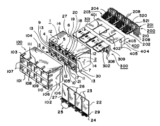
As illustrated in Figs. 1 and 2, the multiport filter
25 connector of the first preferred embodiment of the
invention includes a main dielectric housing 1 having two
rows 2 and 3 of respective openings 4-7 and 8-11, each
arranged to receive an RJ connector plug, and commonly
referred to as ports. Adjacent openings in each row are
30 separated by partition walls 12 which form side walls of
the openings, with the outside sidewalls 13 of the outside
openings 4, 7, 8, and 11 being defined by the side walls 14
of the main dielectric housing 1. The side walls of the
openings include steps 15 for defining notches 16 arranged
35 to receiving latches provided on the standard RJ connector
_g_
CA 02342998 2001-03-08
WO 00/14832 PCT/US99/18823
plugs, as is well known. Each of the side walls also
includes, between the steps 15, a groove 17 for
accommodating a ground tab 108, described below in
connection with the outer shield 100, with the portions of
5 partition walls 12 and outside side walls 13 that extend
vertically between the horizontal rows 2 and 3 having
formed therein three parallel slots 18-20 extending from a
horizontal wont wall section 21 to the rear of the
openings, the slots being open at the rear for receiving,
10 respectively, upper contact modules 200, lower contact
modules 300, and intermediate shielding member 400.
Main dielectric housing member 1 is open at the rear
but is arranged, in known fashion, to receive a rear wall
22 after insertion of the contact assemblies. The rear
15 wall includes ribs 23 that fit between inserted
contact/filter modules, a base portion 24 having openings
for permitting passage of respective contacts extending
downwardly from the contact/filter modules for insertion
into a circuit board on which the connector assembly is to
20 be mounted. Extending inwardly from the base are
trapezoidal tabs 25 which engage corresponding openings at
the rear of the base of the bottom wall of the housing
member (not shown), and extending upwardly from ribs 23 are
tabs 26 that fit within openings 27 in the top wall 28 of
25 the main dielectric member 1, tabs 25 and 26 cooperating to
help hold the rear wall 22 to the dielectric housing 1 upon
assembly of the rear wall to the housing after insertion of
the contact/filter modules and shield. Although not shown,
vertical grooves may be formed in the rear side walls of
30 the main housing for receiving rear wall 22, with dimples
29.serving to provide an interference fit with the side
wall of the main housing and further secure the rear wall
22 thereto. Also shown in Figs. 1 and 2 are mounting posts
30 extending from the bottom wall of the main dielectric
-10-
CA 02342998 2001-03-08
WO 00/14832 PCT/US99/18823
housing member for insertion into openings in the circuit
board on which the connector is mounted.
Shield 100 is preferably made up of a stamped and
formed member which may be similar to the shield described
5 in U.S. Patent No. 5,775,946 (Briones), and which prior to
assembly to the main dielectric housing 1 has been soldered
to form a parallelepiped-shaped structure made up of a
front panel 101, side panels 102 and 103, a top panel 104,
and a rear panel 105, the rear panel being arranged to
10 extend parallel to the top panel until the shield has been
fitted over the housing, after which it is folded to cover
the rear of the housing and secured by latching structures
(not shown) to the housing or to the side panels of the
shield. Extending from side panels 102 and 103 are
15 grounding tabs 106 for insertion into apertures in the
circuit board, and extending from the front panel adjacent
openings 107 are grounding tabs 108 for engaging shields on
the plug connectors to be inserted through apertures 109 in
the front panel and into corresponding openings 4-11 in the
20 main dielectric housing member 1. In addition, shield 100
may include optional external side grounding tabs 110,
lower grounding tabs (not shown), rear grounding tabs (not
shown), and/or top grounding tabs 111 for grounding the
shield to a panel or other conductive structure depending
25 on where the panel or other conductive structure is
situated relative to the connector.
Modules 200 and 300 are similar in structure to each
other but are oriented such that the contacts in module 200
extend downwardly and rearwardly into the corresponding
30 upper openings 4-7 of the dielectric housing 1, and such
that the contacts extend downwardly and rearwardly into the
lower openings 8-11 of housing 1. The vertically mirror
symmetric orientation of the contacts corresponds to the
vertically mirror symmetric arrangement of notches 16 so
35 that the upper openings receive connector plugs with the
-11-
CA 02342998 2001-03-08
WO 00/14832 PCT/US99/18823
latching structure on the upper side of the plugs, and the
lower openings receive the plugs oriented so that the
latching structure is at the bottom of the plugs.
In order to implement the symmetric contact structure,
5 modules 200 and 300 differ in the disposition of the slots
that accommodate the contacts, in the surface to which the
electrical filter and isolation components are mounted, and
in the shape of the contacts, but otherwise are generally
similar. Modules 200 and 300 each have generally L-shaped
10 dielectric bodies 201,301 the horizontal portions 202,302
of which include molded in front contacts 203,2031. The
mating ends 204,304 of the front contacts respectively
extend upwardly and rearwardly at an acute angle, as is
well-known, through slots 205 in a top surface 206 of
15 horizontal portion 202 of module 200, and downwardly and
rearwardly at an acute angle through slots 305 in a lower
surface 306 of horizontal portion 302 of module 300. The
opposite ends of four of the front contacts 203,2031, which
have been bent into an L-shape or after before being molded
20 into the horizontal main body sections 202,302 extend
upwardly from surfaces 206,306 and include terminal
structures 207,307 in the form of notched ends to
facilitate winding of leads of filter components, in a
manner similar to the terminals disclosed in copending U. S .
25 Pat. Appl. Ser. No. 08/866,107.
The remaining four front contacts 2031 are arranged to
form direct solderless connections to resistor chips to be
described below. Advantageously, front contacts 2031 may
be formed as dual contacts in which the angled portions
30 204,304 of a pair of contacts share a single horizontal
rearwardly extending section in order to implement the
connections illustrated in Fig. 13. In the alternative
circuit of Fig. 14, none of the front contacts are paired
and the resistors are omitted.
-12-
CA 02342998 2001-03-08
WO 00/14832 PCT/US99/-18823
I:: addition to the front set of contacts, modules
200,300 are arranged to accommodate rear contacts 208,308.
In module 200, the rear contacts 208 extend downwardly
througr passages 209 in vertical section 210 of the module
5 main body 200. To facilitate positioning of the contacts
in the passages, the contacts include lateral extensions
211 and passages 209 having corresponding enlarged openings
212 at their to. As illustrated, the upper sections 212 of
the rear contacts forwardly at an oblique angle, and
10 include vertical terminal structures 213 in the form of
notched ends to facilitate connection to the filter
components described below.
Because of the different orientation of modules 300,
which are shown upside-down in Fig. 6, rear contacts 308 of
15 module 300 are positioned at the bottom of vertical section
309. dear contacts 308 include vertical sections 310 that
extend vertically from grooves 311 and horizontal sections
312 that are molded into or extend through openings 313 in
the vertical section and include notched terminal portions
20 314 to which leads of the filter components can be wound.
The remaining elements of the modules 200 and 300 are
identical and therefore are given the same reference
numbers. Preferably, the illustrated modules each include
commonly packaged magnetic assemblies X20,521 including
25 transformers and/or inductors having wire leads (one of
which is schematically indicated by the dashed line
labelled 521L1 and a second of which is indicated by the
dashed line labelled 522L2, the remaining wire leads having
been omitted for clarity) extending from the packages and
30 connected to terminal structures 207,307 and 211,312 of the
respective front and rear contacts, as well as to terminal
structures 522 of intermediate contacts 523. By way of
example, each of the magnetic packages can include two
cores corresponding to the inductors and transformers
35 illustrated in the schematic of Fig. 13 (and which may be
-13-
CA 02342998 2001-03-08
WO 00/14832 PCT/US99/18823
similar to those disclosed in U.S. Pat. Appl. Ser. No.
866,107, herein incorporated by reference) or,
alternatively, four cores each, or four packages with two
cores each may be provided, and so forth, depending on the
5 requirements of the filter and isolation circuits. In
addition, the cores can be identical or constructed of
different materials and configurations, and continuously
wound, as disclosed for example in U.S. Pat. Appl. Ser. No.
08/657,209, or separately wound, with or without additional
10 taps. In any case, the magnetic packages are positioned by
upwardly extending structures 524 whose configuration
depends on the shape and dimensions of the magnetic
packages in question, and which may include spindles for
guiding wire leads extending from the magnetic packages to
15 the terminal structures.
While the preferred embodiment of the invention could
be implemented just using magnetic packages, according to
an especially preferred aspect of the preferred embodiment
of the invention, the contact/filter modules further
20 include capacitor and resistor structures. As illustrated
the resistors are in the form of a resistor chip 526 having
a set of four upper electrodes and a set of four lower
electrodes, and a capacitor chip 527 also having an upper
electrode and a peripheral electrode. Resistor chip 526
25 and capacitor chip 527 are seated in slots 528 and 529
molded into respective horizontal sections 202 and 302 of
modules 200 and 300. Extending into the bottom of slot 528
are two contact sections 530, which are integrally formed
with the angled sections 204 of respective pairs of front
30 contacts 2031, as described above, in order to implement
the circuit shown in Fig. 13, and horizontal extensions 531
of the two intermediate contacts 523, with each of contact
sections 530 and extensions 531 engaging one of the four
bottom electrodes of resistor chip 526. Intermediate
35 contacts 523 extend upwardly through slots 532, while
-14-
CA 02342998 2001-03-08
WO 00/14832 PCT/US99/18823
between slots 528,529 and slot 531 is a slot 533 for
accommodating a second intermediate contact structure 534
arranged to electrically connect four upper electrodes of
resistor chip 526 with an upper electrode of the capacitor
5 chip 527.
As a result of this structure, dual front contacts
2031 are connected via two of the resistors formed by
resistor chip 526 to the capacitor chip 527, and the
magnetic packages 520,521 are connected via the remaining
10 two resistors of resistor chip 526 to capacitor chip 527,
thus implementing the circuit shown in Fig. 13.
In an especially advantageous aspect of this
embodiment of the invention, the lower electrode of
capacitor chip 527 is connected to ground via an L-shaped
15 contact 538 extending into the slot S29 from below, and
secured therein by barbs 534, contact 538 including a
horizontal extension 535 with a dimple arranged to engage
the internal ground plate structure 400 described below.
Finally, those skilled in the art will appreciate that
20 the connections between the cores (not shown) provided
within the magnetic packages 520 and 522 are not visible in
Figs. 3-6, but can easily be chosen to correspond to the
connections illustrated schematically in Fig. 13. In
addition, those skilled in the art will appreciate that the
25 arrangement of the components and connecting contacts may
be varied as necessary to implement different circuit
configurations, such as the circuit illustrated in Fig. 14,
which uses the same circuit components as the circuit
illustrated in Fig. 13 (indicated by primed reference
30 numerals), but in which the number of resistors within the
resistor chip is increased (or additional resistors
provided), and in which each of the front contacts is
separately connected to the resistors or magnetic packages.
In order to position the modules 200 and 300 within
35 respective slots or grooves 18 and 19 in the dielectric
-15-
CA 02342998 2001-03-08
WO 00/14832 PCT/US99/~8823
housing 1, each of the modules further includes a track 540
extending laterally from sides of the horizontal portions
202,302 and arranged to slide within slots or grooves 18
and 19 so that the modules can be inserted into the
5 dielectric housing from the rear. As illustrated, the
tracks 540 are provided with dimples 541 for providing an
interference fit with slots or grooves 18 and 19 in order
to secure the modules in the connector.
Assembly of the muitiport connector of this embodiment
10 of the invention is accomplished by first inserting tracks
540 of lower modules 300 into slots 18, and then inserting
intermediate shield 400 into slots 20 and tracks 540 of
upper modules 200 into slots 19 of the dielectric housing
1. The intermediate shield 400 is arranged such that
15 partition walls 6 fit within slots 401 of the shield, slots
401 dividing the shield into panels 402 that extend between
the upper and lower modules 200 and 300, thereby shielding
the upper modules from the lower modules in order to
prevent mutual interference or cross-talk between adjacent
20 contacts in the upper and lower modules. If capacitor chip
527 or other grounded components are included on the
modules, then contacts corresponding to contact 538 will
engage the panels 402 upon assembly of the connector,
connecting the component to ground via vertical extensions
25 including made up of rear panel 403 and side panels 4.04.
Extending from side panels 404 are ground tails 405 for
insertion into corresponding openings on the circuit board
on which the connector is mounted, although those skilled
in the art will appreciate that the shield could also be
30 grounded to the external connector shield, which is also
grounded to the circuit board via grounding tabs 108
described above.
The embodiment illustrated in Figs. 7-12 is identical
to that of Figs. 1-6, except that LED sub-modules are
35 further included. In order to accommodate the LEDs, the
-16-
CA 02342998 2001-03-08
WO 00/14832 PCT/US99/18823
dielectric housing includes openings 600 corresponding to
apertures 601 in the external shield, and the rear panel of
the housing includes openings f.or the LED leads. Because
the construction of the housing, shield, panels, and
5 modules is otherwise identical to that of the embodiment
shown in Figs. 1-6, these elements are not described in
detail in connection with Figs. 7-12.
As in the first preferred embodiment of the invention,
modules 200 and 300 are arranged to provide symmetrical
10 contacts, and thus two different LED sub-modules 700 and
800 are required. The first sub-module 700, shown in
detail in Figs. 9 and 10, consists of a main body 701
having pockets 702 for accommodating LEDs 703, and grooves
704 extending rearwardly for accommodating the leads 705 of
15 the LEDs. The grooves 704 are open at the rear so that the
leads 705 can be bent vertically to extend behind the rear
contacts down through openings in the rear panel into the
circuit board. In order to facilitate mounting of sub-
module 700 onto module 200, sub-module 700 is provided with
20 posts 706 having tabs 707 at the end for insertion into
slots 708 provided in module 200. Alternatively, sub-
module 200 could be supported by posts extending upwardly
from the sub-module and slots or holes in the horizontal
section 706. In addition, at the rear of sub-module 700,
25 as illustrated, is a tab 709 that fits within a slot 710 at
the top of an upwardly extending vertical section 711 of
module 200. Preferably, pockets 702 are provided in
forwardly extending sections 712 that fit within openings
601 in dielectric housing 1 and openings 602 in the shield
30 400.
Sub-module 800 is similar to sub-module 700 and
includes extensions 801 arranged to fit through openings
600 in dielectric housing 1 and openings 601 in shield 100,
and which include pockets 802 for receiving LEDs 803. In
35 this embodiment, the leads 804 of the LEDs extend along
-17-
CA 02342998 2001-03-08
WO 00/14832 PCT/US99/18823
projections 805 and bent downwardly past the ends of the
extensions. Support for the sub-module 800 is provided by
mounting posts 806 having extensions 807 arranged to fit
into holes (not shown) in the top of the sub-module main
5 body 808.
Those skilled in the art will appreciate that the
contact/filte~ modules illustrated in Figs. 7-12 may be
inserted into the dielectric housing _ either with or
without the LSD modules, and that the muitiport connector
10 may include combinations of LED modules with modules that
do not include LEDs, and modules without any filter or
isolation comDOnents, or with different combinations of
components.
In addition, as illustrated in Fig. 15, any of the
15 contact/filter modules described above may be adapted for
use in a single port connector. In the embodiment of Fig.
15, the contact/filter module supports a plurality of lower
front contacts 900 and a plurality of upper front contacts
901 positioned on a main body 902 that forms the base of
20 the connector. Also positioned on main body 902 are a
plurality of rear contacts 903. Some of contacts 900 and
901 have ends that are formed into terminals 904 to which
leads of magnetic packages 905 are connected, for example
according to the schematic illustrated in Fig. 14, and
25 others of contacts 900 and 903 have ends that form contact
tails 906. The opposite end of each of front contacts 900
and 901 are respectively formed into mating sections of the
contacts, while rear contacts 903 all have at their upper
ends terminals 907 to which leads of electrical components
30 may be connected, and contact tails 908 at the lower ends.
Finally, the contact/filter module thus formed is fitted
into a main housing 910 to which a rear housing section 911
is secured in the manner described in U.S. Patent
Application Ser. No. 08/866,107, which discloses the basic
35 principles of providing an RJ connector base having front
-18-
CA 02342998 2001-03-08
WO 00/14832 PCT/US99/18823
and rear contact sections, some of which have ends that are
formed into terminals to which filtering and/or isolation
components may be connected, and others of which are formed
into contact tails. It will of course be appreciated that
5 the main body 902 of this embodiment may include LEDs in a
manner similar to that illustrated in Figs. 7-12.
Having thus described preferred embodiments of the
invention with sufficient particularity to enable those
skilled in the art to easily make and use the invention,
10 and having described several possible variations and
modifications of the preferred embodiment, it should
nevertheless be appreciated that still further variations
and modifications of the invention are possible, and that
all such variations and modifications should be considered
15 to be within the scope of the invention. For example,
while the upper and lower ports may be symmetrically
arranged, it is also within the scope of the invention to
arrange the upper and lower ports to have the same
orientation. Furthermore, instead of grounding the
20 intermediate shield directly to the circuit board, it could
be grounded to the outer shield of the connector and,
instead of mounting the cores on the base of the connector
or on a spindle, the cores could be mounted on a printed
circuit board within the connector, the general concept of
25 using the connector itself to secure the cores could be
extended to apply to filters other than the exemplary
filter illustrated in the drawings, and other circuit
elements could be added to the illustrated circuits. In
addition, it is within the scope of the invention to
30 replace the solderless connections between the various
components on the contact/filter modules, including the
solderless connection between the capacitor and the
intermediate shield, with soldered connections.
-19-
CA 02342998 2001-03-08
WO 00/14832 PCT/US99/18823
Accordingly, the scope of the invention should not be
limited by the above description, but rather should be
interpreted solely in accordance with the appended claims.
-20-