Note: Descriptions are shown in the official language in which they were submitted.
CA 02343241 2003-07-08
Adding DSL Services to a Digital Loop Carrier System
The present invention is related to the field of data communications in the
local access loop of the telephone network. In particular, a system and method
are
disclosed for providing high-speed data and voice services over standard
twisted-
' pair voice-lines in a digital loop carrier ("DLC") system.
In a typical DLC system, the digital transport capabilities of the phone
network are extended from the central office switch into a particular
neighborhood or business location. A remote digital terminal ("ItDT") is
placed
at a remote location from the central office and is connected to it via a
fiber-optic
cable, or some other high-bandwidth connection. The remote digital terminal
receives PCM-modulated voice information from the central office switch,
converts the digital PCM signals into analog voice signals, and routes the
analog
voice signals to a particular customer location via a plurality of line-cards
that
connect the RDT to the customer's location. Similarly, the RDT converts analog
voice information from the customer to a digital PCM format for transport back
to the central office switch. An example of a digital loop carrier system is
set
forth in United States Patent No. 5,046,067 ("the '067 patent', which is
assigned
2 0 to the assignee of the present invention.
The RDT typically includes an interface terminal for communicating
with the central office over the fiber-optic connection, a common equipment
shelf for
WO 00/16587 PCT/US99/20702
-2-
housing equipment that is capable of exchanging PCM voice signals with a
digital switch at the central office and that can also demultiplex high-
bandwidth
signals (such as DS-1 signals) into lower-bandwidth signals (such as DS-0)
signals, and a plurality of copper shelves for housing line-cards (also known
as
channel units). The line-cards convert the PCM digital voice signals from the
common equipment shelf into analog signals, and vice versa, for each customer
that is connected to the RDT.
Dial-up Internet access is a presently available technique for transporting
data to local customers. This mode of data communication transmits digital
data
over an analog voice line using a low-frequency (voice range) modem.
Presently,
the highest-bandwidth that such modems are capable of communicating is about
53 Kbps. This is not sufficient for many Internet applications, such as video-
conferencing, interactive gaming, large file downloads, etc.
Another presently available technique for transporting data to a local user
is via a dedicated digital line, such as a T-1 line, or an ISDN line. Although
these
alternatives provide higher-bandwidth capabilities than an analog modem, they
are very costly to the average consumer, and therefore have met with minimal
market penetration.
Recently, a series of new techniques for transporting data over voice lines,
2 0 known as digital subscriber line (or DSL) have been proposed. DSL
technologies
use advanced digital modulation schemes to transport orders-of magnitude more
information over copper phone lines than analog modems or ISDN lines. The
primary mechanisms for achieving such high throughput are higher-frequency
CA 02343241 2001-03-08
WO 00/I6587 PCT/US99/20702
-3-
transmission and advanced modulation schemes. Because of the promise of
higher transport speeds, DSL is very desirable for Internet applications. In
addition, DSL technology should be available at a fraction of the cost of
dedicated T-1 lines, since no dedicated link is required.
Regardless of what DSL technique is implemented, problems exists with
integrating DSL technology into existing digital loop carrier systems. Power
is
a primary concern. Typical DSL technologies require 4-8 watts per line-card to
operate the complicated modulation algorithms, thus limiting their
applicability
to existing DLC installations, which are power-limited. Limited range is
another
concern. Some customers are at significant distances from the RDT, and if the
DSL line-card range is limited, then additional hardware may be required to
connect to a particular customer that is far from the RDT. Noise introduced
into
the system is yet another concern. But perhaps the most vexing problem is how
to adapt the existing DLC infrastructure to support high-bandwidth digital
data
without reducing the voice-bandwidth capabilities of the system, or without
having to replace the RDT equipment already installed in the field. The
present
invention solves this problem, as well as many others.
Thus, there remains a general need in this field for a system and method
for integrating DSL capabilities into existing DLC systems.
2 0 There remains a more particular need for such a system and method in
which an auxiliary bus is converted into a digital data bus for transporting
data
directly between the interface terminal and the DSL line-cards in the RDT,
CA 02343241 2001-03-08
Image
23.JRN.2001 '14:27 'JONES DAY +49 69 97263993 ~'NR.380 ~S.9i15 '
JO' DAY
a~°~ D~h~ ~s~s 8~am a customer premises to a central ttetvvorlc. This
article is not ralatod, to digital loop carrier sye~ttems arc mochfjr~ing
eadsting remote digital
to~mina! (RDA stxuchues to more effcietitty transport data signals,
~C~F~
?he present invention ovcnco~te$ t~ proh~ nod dove and satires
I~ the weeds is this field fox a digital loop Carrier system that i9 capable
of
transporting both voice and DSL data, s~gnaIs. 'fhe digital loop cax~~ system
includes a remote digital terminal having an intcrFacc terminal, a common
equipment shelf for interfacing .~~~ voice signals ca the oe~l oi~ce switch,
and at least one copper shelf coupled to the common shelf for lmIding ~~oice
Iine
15 cards that convert digital voice signals into analog voice signals (axtd
vice versa)
far trdasport to customer premises, At Least one aopptr shelf fs configured to
include an auxiliary digital data bus (preferably a packst data bus) for
connecting
combination voice/DSL lice-cards and 9t Iea~st one dad uplink card. The data
uptink card is coupled directly to the inte~rfaoc ternainat to enable DSL data
CA 02343241 2001-03-08
CA 02343241 2003-07-08
transport without impacting digital voice capabilities through the common
equipment. Also disclosed is an optional Ethernet switch in the remote digital
terminal for concentrating multiple DSL signals prior to transport back to the
central office.
S As described in more detail below, the present invention can be used with
any DSL modulation scheme. However, because of the inherent power limitations
of existing DLC installations, the preferred embodiment of the present
invention
uitlizes a low-power QPSK-modulation technique. It is to be understood that
this
is only one example of the many types of modulation schemes that could be
integrated into the combination voice/DSL line-cards, and the overall system
of
the present invention.
In accordance with another aspect of the present invention, there is
provided a system for transporting voice and data signals in the local
telephone
loop, comprising:
a central office switch configured to transmit and receive voice and data
signals;
a plurality of customer interface devices for communicating voice and data
signals to and from the central office switch; and
a remote digital terminal (RDT) coupled between the central office switch
and the customer interface devices, the RDT comprising:
an interface terminal for communicating voice and data signals
between the central office switch and the RDT;
a common equipment shelf coupled to the interface terminal for
transmitting and receiving voice signals; and
CA 02343241 2003-07-08
6
at least one copper equipment shelf coupled to the common
equipment shelf, the copper equipment shelf including a plurality of
communication cards and a digital data bus for transporting data signals
between the communication cards,
wherein at least one of the communication cards is a data uplink card
coupled directly to the interface terminal for transmitting and receiving data
signals, and at least one other of the communication cards is a combination
voice/data communication card for simultaneously transmitting and receiving
voice and data signals between at least one of the customer interface devices
and
the RDT, and wherein the voice signals are routed to and from the interface
terminal through the common equipment shelf and the data signals are routed to
and from the interface terminal through the data uplink card.
In accordance with another aspect of the present invention, there is
provided a system for transporting voice and data signals in the local
telephone
1 S loop, comprising:
a central office switch configured to transmit and receive voice and data
signals;
a plurality of customer interface devices for communicating voice and data
signals to and from the central office switch; and
a remote digital terminal (RDT) coupled between the central office switch
and the customer interface devices, the RDT comprising:
an interface terminal for communicating voice and data signals
between the central office switch and the RDT;
a common equipment shelf coupled to the interface terminal for
CA 02343241 2003-07-08
7
transmitting and receiving voice signals; and
at least one copper equipment shelf coupled to the common
equipment shelf, the copper equipment shelf including a plurality of
communication cards and a digital data bus for transporting data signals
between the communication cards,
wherein at least one of the communication cards is a data uplink card
coupled directly to the interface terminal for transmitting and receiving data
signals, and at least one other of the communication cards is a combination
voice/data communication card for simultaneously transmitting and receiving
voice and data signals between at least one of the customer interface devices
and
the RDT, and wherein the voice signals are routed to and from the interface
terminal through the common equipment shelf and the data signals are routed to
and from the interface terminal through the data uplink card.
In accordance with another aspect of the present invention, there is
provided an improved digital loop carrier system including a remote digital
terminal (RDT) having an interface terminal, at least one common equipment
shelf for interfacing digital voice signals to a central office switch via the
interface
terminal, and at least one copper shelf coupled to the common shelf for
housing
line-cards that convert digital voice signals into analog voice signals for
transport
to customer locations, the improvement comprising:
at least one combination voice/data line card housed in the copper shelf for
communicating voice and data signals to a customer location;
at least one data uplink card housed in the copper shelf for communicating
data signals to the combination voice/data line-card; and
CA 02343241 2003-07-08
g
a digital data bus for connecting the combination voice/data line card to
the data uplink card;
wherein the digital voice signals are routed between the combination
voice/data line card and the interface terminal via the common equipment shelf
and the data signals are routed between the combination voice/data line card
and
the interface terminal via the data uplink card.
The present invention provides many advantages over presently available
techniques for transporting voice and digital data in the local loop,
particularly
when applied to DSL transport over existing DLC system. Not all of these
advantages are simultaneously required to practice the invention as claimed,
and
the following list is merely illustrative of the type of benefits that may be
provided, alone or in combination, by the present invention. These advantages
include: (1) existing DLC systems can be easily and cost-effectively upgraded
to
the present invention; (2) the preferred QPSK modulation scheme provides low
power in comparison to other presently known DSL techniques; (3) voice and
data
services are combined on a single line-card; (4) DSL data services can be
added or
designed-into a DLC system without impacting the voice carrying capabilities
of
the system; (5) DSL data can be combined at the RDT prior to
WO 00/16587 PCT/IJS99/20702
-9-
transmission to the central office switch; and (6) different types of DSL
technologies can be integrated into the same DLC system.
These are just a few of the many advantages of the present invention, as
described in more detail below. As will be appreciated, the invention is
capable
of other and different embodiments, and its several details are capable of
modifications in various respects, all without departing from the spirit of
the
invention. Accordingly, the drawings and description of the preferred
embodiments set forth below are to be regarded as illustrative in nature and
not
restrictive.
DRIEF DESCRIPTION OF THE DRAWINGS
The present invention satisfies the needs noted above as will become
apparent from the following description when read in conjunction with the
accompanying drawings wherein:
FIG. 1 is block diagram of a preferred digital loop carrier system capable
of transporting voice and DSL data services in the local loop;
FIG. 2 is a preferred backplane structure diagram of one copper shelf in
the remote digital terminal of the system in FIG. 1, including an auxiliary
packet
data bus;
2 0 FIG. 3 is block diagram of a preferred combination voice/DSL line-card
installed in one of the copper shelves of the remote digital terminal
connected to
a corresponding network interface device ("NID") at the customer premises for
delivering voice and DSL data services over a single copper pair;
CA 02343241 2001-03-08
WO 00/16587 PCT/US99/20702
-10-
FIG. 4 is an expanded block diagram of the preferred combination
voice/DSL line-card in FIG. 3;
FIG. 5 is an expanded block diagram of the preferred NID corresponding
to the preferred combination voice/DSL line-card in FIG. 3;
FIG. 6 is a circuit schematic showing the termination scheme of the
auxiliary packet data bus set forth in the backplane structure diagram of FIG.
2,
and a corresponding timing diagram; and
FIG. 7 is a bus state machine diagram of the auxiliary packet data bus.
Zo DETAILED DESCRrPTION OF THE D AWINGS
Referring now to the drawings, Figure 1 sets forth a block diagram of a
preferred digital loop carrier system capable of transporting voice and DSL
data
services in the local loop. This system includes central office equipment 12,
at
least one remote digital terminal 10, and customer premises equipment 14. The
central office equipment 12 includes at least one source of voice information
30,
such as POTS ("Plain Old Telephone Service") lines from a local digital switch
(not shown), at least one source of digital information 34, and a fiber optic
terminal 28 connected to the voice traffic and data traffic information 30,
34. The
POTS lines 30 provide a source of voice information, and are typically PCM-
2 0 modulated DS-0 or DS-1 lines, but could be other sources of voice
information.
The source of digital information could be a 10 Base-T data source, such as
from
an Internet server, or could be a DS-1 frame relay or ATM signal. The fiber
optic
terminal 28 couples the voice and data traffic to at least one fiber optic
cable 40
CA 02343241 2001-03-08
CA 02343241 2003-07-08
-11-
for distribution to the remote digital terminals) 10 of the DLC system. (Refer
to United States Patent No. 5,046,067, for a more detailed description of
this type of equipment.)
As described in the background section of this application, the purpose of
the digital loop carrier system is to extend the digital signal capabilities
of the
digital telephone network, which typically ends at the central office switch
12,
into the field to a point closer to the customer premises 14. This provides
numerous advantages, the primary one being that only a few number of optical
fibers need to be extended out from the central office instead of thousands of
pairs of copper wires, due to the high-bandwidth signal capacity of the fiber.
Presently available digital loop carrier systems are primarily designed to
transport
PCM digital voice signals to and from the central office on the one hand, and
analog voice signals to and from the customer premises on the other hand. The
bandwidth of information capable of being transported by the digital loop
carrier
system is typically constrained by the capabilities of the common equipment in
the RDT that interfaces to the PCM-modulated voice information from the
central
office. The voice-bandwidth of the RDT would be further constrained if high-
speed data cards were added to the system. Although this is possible to do
with
existing DLC systems, it would mean a reduction in the PCM voice-carrying
2 0 capabilities of the network, which is undesirable.
The present invention shown in Figure 1 overcomes this problem by
configuring an auxiliary bus in the remote digital terminal 10 as a special
packet
data bus, and by routing digitally modulated data signals, such as DSL data,
WO 00/16587 PCT/US99/20702
-12-
directly from the customer premises equipment 14 to the central office and
bypassing the common equipment 20 of the RDT 10. In this manner, DSL
capabilities can be added to an existing DLC system without impacting the PCM
voice-carrying capabilities of the network. As described in more detail below,
the present invention provides many other benefits and enhancements over
presently known DSL delivery systems in the local loop.
The preferred DLC system shown in Figure 1 includes at least one remote
digital terminal 10, although it could include many such terminals. The RDT 10
includes a fiber-optic interface terminal 16, an optional Ethemet switch 18,
at
least one common equipment shelf 20, one or more copper shelves 22, each
copper shelf including a plurality of slots 24 for receiving line-cards and a
backplane (not shown in this figure) that each line-card plugs into, and one
or
more ribbon cables 26 that couple the copper shelf 22 to the common equipment
shelf 20.
In a typical DLC system, the PCM voice data from the central office 12
is received from the fiber optic line 40 by the fiber-optic interface terminal
16 and
converted from an optical signal, such as an OC-3 signal, into an equivalent
electrical signal. This signal is then routed to the common equipment as one
or
more DS-1 signals, or a DS-3 signal, or some other equivalent electrical
signal.
2 0 The common equipment shelf 20 typically includes termination points for
the
DS-1 signals from the central office, each DS-1 providing 24 DS-0 PCM-
modulated phone links. These DS-0 voice channels are then distributed to the
various line-cards in the one or more copper shelves 22 via ribbon cables 26.
The
CA 02343241 2001-03-08
WO 00/16587 PCT/US99/20702
-13-
common equipment shelf also includes power circuitry for powering the common
equipment as well as the copper shelves 22, circuitry for detecting when a DS-
1
line has failed, and circuitry for handling system alarms and maintenance,
troubleshooting functions, inventory control functions, testing, and many
other
functions that are central to the DLC system. The '067 patent provides further
information on this functionality.
The fixed-bandwidth of the common equipment shelf 20 determines how
much voice information can be carried through a particular RDT via the line-
cards plugged into the one of more copper shelves 22. Each copper shelf 22 is
a chassis that includes a backplane having many traces and a plurality of
multi-
pin connectors into which the line-cards are plugged. The same traces on the
copper shelf backplanes are also preferably connected to the common equipment
shelf 20 via the various ribbon cable connections 26. In this manner, the
common
equipment 20 can communicate PCM voice signals to any of the line-cards in any
of the copper shelves 22.
Preferably, there is one line-card (or channel card) for each customer
premises 14. The PCM voice signals for a particular customer are routed from
the common equipment shelf 20 over the ribbon cable 26 to the backplane of a
copper shelf 22, and then to the line-card for the particular customer. The
Iine-
2 0 card converts the PCM digital voice information into an analog voice
signal and
routes that signal on a twisted-pair copper connection 38 to the customer
premises 42. At the customer premises, the analog voice signal is typically
terminated at a network interface device ("1VID") 42 and routed to the
telephones
CA 02343241 2001-03-08
WO 00/16587 PCT/US99/20702
-14-
(or other customer interface devices) on the customer's premises. Also shown
in
Figure 1 is a copper cross-connect 36. This is a wiring distribution box that
cross-connects a large number of bundled twisted-pair connections from the RDT
to numerous smaller bundles of connections for local routing.
The present invention improves upon this existing DLC architecture for
routing voice signals by providing the one or more copper shelves 22 with an
auxiliary digital bus that is preferably configured as a digital packet data
bus, and
by providing two types of special data cards, a combination voice/DSL line-
card
and a digital data uplink card. The configuration of the digital packet data
bus
and its operation are described in connection with Figures 2, 6 and 7, below,
and
a preferred QPSK-modulation voice/DSL line-card is described in connection
with Figures 3, 4 and 5.
The combination voice/DSL line-card 52 and the digital data uplink card
91 plug into the one or more copper shelves. There is one combination
voice/DSL line-card 52 for each customer that wants not only voice service,
but
high-speed DSL service as well. It is important to note at this point that
although
the preferred modulation scheme described in this application is a QPSK
scheme,
the present invention includes any type of DSL modulation, including, but not
limited to discrete mufti-tone ("DMT"), Garner-amplitude and phase modulation
2 0 ("CAP"), or multiple-virtual line ("MVL"). These are just a few of the
presently
known DSL modulation schemes that could be incorporated into line-cards for
use with the present invention. The primary reason that QPSK modulation is
disclosed as the preferred embodiment is because it is a very low-power
CA 02343241 2001-03-08
WO 00/16587 PC'T/US99/20702
-15-
modulation scheme, and for large RDT installations that could have as many as
2000 line-cards, power-consumption is a critical issue for successful
deployment
of a DSL system.
The digital data uplink card 91 could be either a DS-1 or Ethernet (or
some other type o~ uplink card that communicates over the auxiliary packet
data
bus on the backplane of the copper shelf 22 to the various combination
voice/DSL line-cards 52. This card 91 is coupled to the fiber optic interface
terminal so as to provide a digital data transport path 32 that bypasses the
PCM
voice circuitry of the common equipment shelf and therefore does not impact
the
PCM voice-carrying capabilities of the RDT. The packet data transported over
the packet data bus from the voice/DSL line-cards is converted by the uplink
card
91 into a DS-1 format, or could simply be passed along to an optional Ethernet
switch 18, if the data packets are already in Ethernet format. The purpose of
the
optional Ethernet switch 18 is to concentrate 10 Base-T level signals from
various
uplink cards prior to communication over the optical fiber 40, in order to
optimize bandwidth. The output of the optional Ethernet switch 18 is
preferably
a DS-1 or DS-3 signal, but it could, alternatively, be a 100 Base FX signal
over
fiber 40, or a separate fiber (not shown) back to the central office, or it
could be
a wavelength-division multiplexed signal ("WDM") over the same fiber 40 as the
2 0 PCM voice information is transmitted.
By providing a special-purpose digital packet data bus and special-
purpose line-cards for transporting both voice and DSL signals over the copper
shelf backplane, and by bypassing the conunon equipment shelf 20 for the DSL
CA 02343241 2001-03-08
WO 00/16587 PCT/US99/20702
-16-
data, the present invention provides the ability to add high-speed DSL
capabilities
to the existing DLC infrastructure without impacting the PCM voice carrying
capabilities of the system.
Assuming that the system in Figure 1 is configured as described above
with the digital packet data bus and the special-purpose line-cards, the
twisted-
pair copper connections 38 to the customer premises 14 can then be used to
transport both low-bandwidth voice signals and high-bandwidth DSL data
signals. These signals are terminated at the NID 42, which may include a
splitter
44 for splitting the voice information from the data information, and a DSL
modem 46 for demodulating the DSL signal into some other electrical signal
that
is compatible with a typical computer interface 50. The voice signal is routed
to
the internal phone connections 48. Having the splitter 44 and modem 46 in the
NID is optional. In some forms of DSL, such as the so-called "g.lite"
modulation, a splitter is not needed. Alternatively, the splitter could be
external
to the NID, or it could be incorporated into some type of DSL terminal that
includes the splitter and the modem. This equipment could be either inside the
computer 50, or connected nearby. The exact configuration of the NID and the
customer premises equipment is not important to the present invention. It is
only
described in order to convey a complete understanding of the inventive system.
2 0 Figure 2 is a prefer ed backplane 56 structure diagram of one copper shelf
22 in the remote digital terminal 10 of the system in Figure 1, including pins
68
that form the auxiliary packet data bus over which the DSL data packets are
transported from the combination voice/DSL line-cards to the data uplink
cards.
CA 02343241 2001-03-08
WO 00/16587 PC'T/US99/20702
-17-
The preferred copper shelf 22 includes a backplane 56 having numerous
connections. As shown in figure 2, there are preferably 54 connections,
although
the number of connections could be higher or lower depending on the
application
and the particular DLC system. There are preferably 48 slots in each copper
shelf
for receiving line-cards 52, although, alternatively there could be any number
of
slots. Each line-card 52 plugs into the chassis and the backplane 56 of the
copper
shelf 22 via a connector 54. This connector preferably includes 54 connections
that match with the 54 connections of the backplane 56. Again, these numbers
are arbitrary, and are only described for purposes of the exemplary system
shown
1 o in the drawings.
The 54-pin backplane preferably includes eight ground signals 62, ten
power signals 64, two ringing voltage signals 66, a twelve-pin test bus 68,
two-
pins for system-clock and sync 70, four pins for the Channel Unit Data Link
("CUDL") and DPCM information 72 (refer to the '067 patent for more
information on these signals), eight pins for the PCM voice signals 74-80,
eight
pins for the tip/ring signals 82, and six pins for physical address 84. These
bus
signals on the backplane 56 are connected externally to the copper shelf by
power
cable 58, ribbon cable 26, and drop cable 60. The power cable 58 and the
ribbon
cable 26 are preferably connected to the common equipment shelf 20. The
digital
2 0 PCM voice information is transported between the common equipment shelf 20
and the copper shelf 22 via the ribbon cable 26. These voice signals are then
routed over the backplane 56 to the appropriate line-cards 52 for conversion
to
analog signals and transport to the customer premises.
CA 02343241 2001-03-08
WO 00/16587 PCTNS99/20702
-18-
The test bus 68 is an auxiliary bus. It does not normally function to
provide active services to customers, but is only used in certain situations
where
a system problem has occurred that requires testing. At least 4 of the test
bus
pins are not used at all. Therefore, this bus is the type of connection that
could
be configured to provide another fimction. In the present invention, this
function
is the digital packet data bus that connects the combination voice/DSL line-
cards
to the digital data uplink cards.
Although a particular type of packet data bus is preferably used with the
present invention, as described in more detail below with reference to figures
6
and 7, it is to be understood that other types of digital bus protocols could
be
implemented using these pins, such as a mufti-point HDLC (High-level Data Link
Control) signaling scheme. HDLC is a bit-oriented, synchronous protocol that
applies to the data-link layer (layer 2 of the ISO/OSI model) for computer-
microcomputer communications. Messages in HDLC are transmitted in units
called frames, which can contain differing amounts of data but which are
organized in a particular way. This is just one additional example of the type
of
signaling scheme that could be implemented to transfer the DSL digital
information.
Although in the preferred embodiment an existing bus (i. e. the test bus)
2 0 is configured as a digital packet data bus, alternatively, the system of
the present
invention could be designed from the beginning to include a special-purpose
digital data bus on the copper shelf backplanes 56 that enable data to be
routed
directly to the interface terminal 16 and bypassing the common equipment shelf
CA 02343241 2001-03-08
WO 00/16587 PCT/US99/20702
-19-
20. Or, alternatively, a special digital data bus could be implemented through
the
ribbon cable connecting the copper shelves to the common equipment shelf and
special digital packet data handling circuitry could be built into the common
equipment. Other embodiments and configurations of the digital packet data bus
are possible and are within the scope of the invention.
Turning now to Figures 3, 4 and 5, these figures show a preferred example
of implementing DSL over voice lines using QPSK modulation. As noted
previously, the use of QPSK modulation as the DSL scheme is only the preferred
embodiment of the invention and unless specifically limited, the claims and
1 o coverage of this application are not limited to any particular DSL
technology.
QPSK, or Quadrature Phase Shift Keying is a modulation scheme that is known
in the art. The exact details of this scheme will not be described herein
since they
are known to one of ordinary skill in this art, as are the other DSL
modulation
schemes mentioned in this application, such as DMT, QAM, MVL, and others.
(For more information on DSL modulation schemes, refer to Leon W. Couch II,
Digital and Analog Communication Systems, Macmillan Publishing, 1993, in
particular the following pages -- QPSK at pp. 387-388, 391-393; QAM at pp.
389-393; PCM at pp. 142-145; HDLC at pp. 776-77; etc.) A key advantage to
using QPSK, particularly in conjunction with the present invention, is that it
is
2 0 an inherently low power technology. In addition, a high signal-to-noise
ratio is
not required in QPSK. This is very important for telephony applications were
noise immunity is typically a limiting factor.
CA 02343241 2001-03-08
WO 00/16587 PCT/US99/20702
-20-
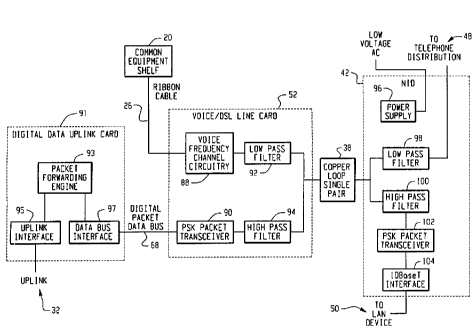
Figure 3 is a block diagram of the connections between a preferred
combination voice/DSL line-card 52 installed in one of the copper shelves 22
and the NID 42 at the customer premises, on the one hand, and the digital data
uplink card 91 and the common equipment shelf 20, on the other hand. The
purpose of the combination voice/DSL line-card 52 is to convert and transport
voice and data information back and forth between the customer premises
equipment 52 and the voice and data interface equipment 91, 20 in the RDT.
Figure 4 is an expanded block diagram of the preferred combination voice/DSL
line-card 52 in Figure 3, and Figure 5 is an expanded block diagram of the
preferred NID 42 corresponding to the preferred combination voice/DSL line-
card 52 shown in Figure 3.
Figure 3 shows the preferred combination voice/DSL line-card 52
according to the present invention. This card 52 plugs into the backplane 56
of
one of the copper shelves 22. The PCM digital voice information coming into
and going out from this card is transported over backplane pins 74-80 to the
ribbon cable 26 and onto the common equipment shelf 20, where this information
is combined with other PCM data and passed onto or received from the fiber
interface terminal 16. The QPSK-modulated DSL data is transported over the
auxiliary data bus pins 68, which have been configured to operate as a packet
data
2 o bus, to the digital data uplink card 91.
The digital data uplink card 91 preferably includes a data bus interface 97
for interfacing to the digital packet data bus 68, an uplink interface 95 for
interfacing either to the fiber optic terminal 16 of the RDT or to an optional
CA 02343241 2001-03-08
WO 00/16587 PCT/US99120702
-21-
Ethernet switch 18 via uplink 32, and a packet forwarding engine 93 for
managing the transport of data packets to and from the combination voice/DSL
line-cards 52 and the uplink interface 32. The packet forwarding engine 93
also
manages the conversion of packets from Ethernet to DS-1 and vice versa, in the
case where the uplink 32 is directly coupled to the fiber optic terminal 16,
and
may also be capable of converting from one packet type to another in the case
where the format of the data on the digital packet data bus 68 is not already
in
Ethernet format. The packet forwarding engine 93 could be either an embedded
microprocessor or microcontroller (including associated memory and support
1 o circuitry) operating under software control, or, alternatively could be
implemented as an FPGA or other programmable logic device for higher-speed
operation.
The preferred combination voice/DSL line-card includes a connector 54
for interfacing the card to one of the backplanes 56 in one of the copper
shelves
22, voice frequency channel circuitry 88, a QPSK packet transceiver 90, a low
pass filter, and a high pass filter 94. The voice frequency channel circuitry
converts the PCM digital voice information from the PCM data lines on the
backplane 74-80 into analog signals and transports them through low-pass
filter
92 (to remove high-frequency components that could disturb the DSL signals)
2 0 onto a copper-loop single twisted-pair 3 8 to the 1VID 42 at the customer
premises.
The QPSK packet transceiver 90 receives and transmits DSL modulated
data (preferably in QPSK form, but alternatively in any other high-frequency
CA 02343241 2001-03-08
WO 00/16587 PCT/US99/20702
-22-
digitally modulated fashion) between the I~TID and the auxiliary digital
packet
data bus 68 of the copper shelf backplane 56. Once on the packet data bus,
this
information is routed to a digital data uplink card and then coupled onto the
central office via the fiber optic terminal 16 and the fiber cable 40
connecting the
remote digital terminal 10 to the central office. The DSL information could be
converted into either a DS-1 type signal, or an optional Ethernet packet,
prior to
coupling to the fiber optical interface terminal 16. The high-pass filter 94
prevents the QPSK circuitry from interfering with the voice circuitry. In this
manner, a special-purpose combination card is provided that includes both low-
1 o frequency voice-channel capabilities and high-frequency DSL capabilities
in a
single line-card.
At the other end of the twisted-pair connection 38 is the customer
premises 14. This may include a NID 42 that may in turn include circuitry for
interfacing with the combination voice/DSL line-card 52. Alternatively this
circuitry could be external to the 1VID, closer to the customer's interface
devices
(telephone, fax machine, computer, etc.) The interface circuitry includes a
low
pass filter 98, a high-pass filter 100, a QPSK packet transceiver 102, and,
optionally, a 10 Base-T interface 104. Also shown in the 1VID 42 is an
optional
power supply 96 that is connected to a low voltage AC source at the customer
2 o premises. This power supply 96 converts the 120VAC line voltage from the
customer's premises into a set of DC voltages for operating the equipment in
the
IVID.
CA 02343241 2001-03-08
WO 00/16587 PCT/US99/20702
-23-
The low-pass filter 98 filters away the high-frequency DSL information
and only passes the lower-frequency analog voice information for distribution
to
the internal telephone network 48 at the customer location. Similarly, the
high-
pass filter 100 filters away the low-frequency voice information and only
passes
the higher-frequency DSL data information. This DSL data is then converted
into
some non-modulated form, such as 10 Base-T Ethernet packets, or some other
type of signal, by the QPSK packet transceiver 102. The filters and
transceiver
in the NID are similar in design to those in the combination voice/DSL line-
card
52. The output of the QPSK transceiver 102 is then passed on to an optional 10
Base-T Ethernet interface, or some other type of digital interface, for
distribution
to an internal LAN, such as an Ethernet network, or for direct connection to a
computer, fax machine, or other device. As noted above, all of the circuitry
shown in the NID could be external to this device, and, in particular, could
be
installed in an external or internal device located in a computer or other
device
within the customer premises.
Figure 4 shows an expanded block diagram of the circuitry in the
preferred combination voice/DSL line-card. This circuitry includes the QPSK
packet transceiver 90, high-pass filter 94, low-pass filter 92 and voice
frequency
channel circuitry 88, which have been discussed. Also shown in this diagram
are
2 0 the connections to the copper shelf backplane 56 on the one hand, and the
copper
loop single twisted pair 38 on the other. This diagram is expanded to show
that
the preferred QPSK packet transceiver includes a Field Programmable Gate Array
("FPGA") I 10, a memory buffer 112, a configuration EPROM 118, a receiver
CA 02343241 2001-03-08
WO 00/16587 PCTNS99/20702
-24-
114 and a transmitter 116. Also shown in this diagram is an Aux. Bus interface
circuit 108 (shown in more detail in Figure 6), and a channel card FPGA 106.
PCM voice information is transported in the upper path of the card 52,
and DSL digital data is transported in the lower path. Voice information from
the
PCM pins on the backplane 56 is connected to the channel card FPGA 106,
which is a controller that determines whether the data is for this particular
card,
and includes circuitry for extracting voice information from the bus and
transmitting information back onto the bus. From the channel card FPGA 106,
the extracted voice information is passed to the voice-frequency channel
circuitry
88, which, as noted above, converts the PCM digital voice information from the
PCM data lines on the backplane 74-80 into analog signals and transports them
through low-pass filter 92 (to remove high-frequency components that could
disturb the DSL signals) onto a copper-loop single twisted-pair to the 1VID 42
at
the customer premises. In similar fashion, analog voice information from the
customer premises 42 is transported over the copper-loop single twisted-pair
38
to the card 52, is filtered 92, converted into a digital PCM signal and
transmitted
onto the backplane 56.
The digital DSL information is transported on the lower path. First we
will consider the forward path, where information is being transmitted from
the
2 0 central office switch 12 to the customer premises 14 through this
combination
line-card 52. The digital information from digital source 34 is transmitted on
fiber 40 to the fiber optic terminal 16 of the RDT 10. From here, the
information
is preferably downlinked 32 as a DS-1 signal to a digital uplink data card 91
CA 02343241 2001-03-08
WO 00/16587 PCT/US99/20702
-25-
installed in one of the copper shelves 22. (Although, as noted in Figure 1,
this
information could be converted into some other format, such as Ethernet,
within
the RDT, and then routed to the digital data uplink card 91 as a l OBase-T
type of
signal.) The uplink card 91 then broadcasts this information onto the
auxiliary
data bus 68 in packet bursts. These packets are routed to the proper line-card
52
and are received by auxiliary bus interface circuitry 108.
Once on the card, these packets are then transmitted to the FPGA 110.
The FPGA 110 provides many functions. It controls the receipt and transmission
of DSL data through the card by communicating with receiver 114 and
l0 transmitter 116. Various signals such as "level detect," "blank (xmit),"
"gain
control," "equalize," and "hold" are used to control these circuits. The FPGA
110 also controls the conversion from packet data (or whatever form of data is
being transmitted on the auxiliary data bus) to DSL-modulated data. The
preferred DSL modulation scheme is QPSK. The QPSK modulated data is then
transmitted via transmitter 116, through high-pass filter 94 and onto the
copper
loop single twisted-pair 38. The frequency of transmission of this QPSK signal
is on the order of 320 KB/s, which is roughly an order of magnitude greater
than
current analog modem technologies. The FPGA also utilizes an external
memory 112, which is used as a store-and-forward buffer for the DSL data, and
2 o a configuration EPROM 118, which stores software-reprogrammable
configuration information for the DSL part of the line-card 52.
Going in the opposite direction, QPSK-modulated data from the customer
premises is filtered by band-pass filter 94, received by receiver 114, and
then
CA 02343241 2001-03-08
WO 00/16587 PCT/US99/20702
-26-
converted into a non-modulated digital packet data format by FPGA 110 and
transmitted out on the auxiliary data bus 68 through bus interface circuitry
108.
A state diagram showing the method of operation of the FPGA as it
communicates data over the auxiliary packet data bus is shown in Figure 7.
Figure 5 is an expanded block diagram showing the corresponding
voice/DSL circuitry in the 1'IID 42 at the customer premises 14. This
circuitry
includes low-pass filter 98, band-pass filter 100, QPSK packet transceiver
102,
power supply 96, 10 Base-T transceiver 104 and line interface 120. The low-
pass
filter 98 passes the low-frequency analog voice information to and from the
customer telephone equipment 48. The band-pass filter 100 passes the high-
frequency QPSK DSL data signal to and from the customer digital data
equipment 50 through the QPSK transceiver 102, 10 Base-T transceiver 104 and
line-interface 120.
The circuitry in the QPSK transceiver 102 includes an FPGA 124, which
corresponds fimctionally to the FPGA 110 in the voice/DSL line-card 52, a
receiver 126, transmitter 128, a buffer memory 130, and a configuration EPROM
122. These circuits operate in a manner similar to those in the voice/DSL line-
card 52. The QPSK DSL information is received by receiver 126, and then is
demodulated and converted into a digital data stream, such as a 10 Base-T
2 0 Ethernet packet stream, by the FPGA 124. This 10 Base-T data is then
transmitted to the customer's digital data equipment 50. Similarly, 10 Base-T
digital data is converted by the FPGA 124 into QPSK modulated data and
CA 02343241 2001-03-08
WO 00/16587 PCT/US99/20702
-27-
transmitted via transmitter 128 out onto the copper loop single twisted-pair
38
and then to the corresponding line-card 52 at the RDT.
Figure 6 is a circuit schematic showing the termination scheme of the
auxiliary packet data bus set forth in the backplane structure diagram of
Figure
2, and a corresponding timing diagram.
Figure 7 is a corresponding bus state machine diagram. As shown in Figure 6,
the auxiliary packet data bus 68 consists of four pins labeled OTDR[3:OJ 142.
Because there are 8 bits to transfer on the bus for each data byte in a
typical
packet (which preferably consists of 64 bytes), the data is transferred on two
half
cycles of the system clock (SCLK) 140, which is preferably a 1.544 Mbit clock.
The most-significant nibble is transferred in the positive half of the clock
cycle
and the least-significant nibble is transferred in the negative half. The
preferred
digital packet data bus implemented according to Figures 6 and 7 is a
collision
domain bus in which 64 byte packets are transmitted, although, alternatively,
other packet sizes could be utilized.
Each line-card that is connected to the auxiliary packet data bus 68 is
configured with a pull-up network 108 as shown in Figure 6. This network
includes two inverting buffers 132, 134 connected to OUTx and INx signals,
where the OUTx signal is the signal driven onto the bus, and the INx signal is
the
2 0 signal read from the bus, and a pull-up resistor 136 connected between the
buffers
and a high voltage (VCC). The OTDRx signal is the connection to the auxiliary
data bus.
CA 02343241 2001-03-08
WO 00/16587 PC'T/US99/20702
-28-
The auxiliary data bus is 4 bits wide in the preferred embodiment, but
could, alternatively be less than or greater than this number. Line-cards
connected to the bus can start a packet at any time. The state machine
circuitry
implemented in the FPGA on each card will monitor the bus signal for
collisions
and stop transmitting immediately if the bus does not match with what is being
transmitted. When a collision is detected, the line-card waits for an idle
flag plus
a delay before attempting retransmission. Packets that are less than 64 bytes
will
be dropped. There are several flags that are used in the data bus protocol.
These
are: OxFF = idle flag; Ox 1 B = escape flag; and 0x01 = start flag.
Figure 7 sets forth an exemplary state machine, implemented in the FPGA
110 of the line-cards, for transmitting and receiving data on the auxiliary
packet
data bus. When a card is plugged into the chassis of a copper shelf 22 it
powers-
up in a reset WAITIDLE state 144. In this state, the card is simply waiting
for
the idle flag to appear on the bus. This is to prevent a new card from doing
anything that might disrupt the transmission of a current packet. Once an idle
flag is detected, the card moves to the IDLE state 146, and now it is prepared
to
either transmit or receive data from the bus. If the start flag is detected,
then data
is being transmitted on the bus by another card, such as a data uplink card.
In this
case, the card moves into the WRTCHK state 158. In this mode, the card is
2 0 writing data from the bus into a local memory 112. If 64 consecutive bytes
are
received, then the card moves into the WRT state, indicating that one complete
packet has been received. If, prior to 64 bytes being received in the WRTCHK
state, another flag appears on the bus, such as another start flag or an
escape flag,
CA 02343241 2001-03-08
WO 00/16587 PCTIUS99120702
-29-
then a "runt' packet has been detected. Runt packets are generally caused by
collisions (i.e., more than one card trying to transmit data at the same time)
or
short packets. If a runt packet is detected, then the card cycles back to the
IDLE
state 146, and waits for the beginning of another transmission or a message to
transmit onto the bus.
Assuming 64 bytes were received, the card is in the WRT state 160. From
this state, an idle flag would be the next expected signal on the bus. If an
idle
flag is detected after the 64-byte transmission, this indicates a valid
packet. The
card then moves to the WRTIDLE state 162. In the WRTIDLE state, a valid
packet has been received, and this information is then moved out of memory and
processed by the FPGA on the line-card. For example, if it is a packet to be
transmitted to the customer premises, the FPGA would modulate the packet data
using whatever DSL scheme is implemented in the card, and would then transmit
this information onto the twisted-pair connecting the line-card to the
customer
premises. From the WRTIDLE state 162, control of the bus state machine reverts
back to the IDLE state 146. If additional data was received while the card was
in the WRT state 160, i.e. instead of an idle flag, more data were received,
then
an overflow condition has occurred, and control of the bus state machine
reverts
back to the WAITIDLE state 144, waiting for an idle flag to indicate that the
bad
2 0 data has been flushed from the bus. In this situation, any data stored in
the buffer
memory would be discarded.
Writing data to the bus begins when the card detects a non-zero value in
a variable, such as a message counter. At this point, the card moves from the
CA 02343241 2001-03-08
WO 00/16587 PCT/US99/20702
-30-
IDLE state 146 to the WRTDRV 1 state 148. This could be triggered by, for
example, data arnving from the customer premises. This data is written to the
buffer memory 112 of the line-card 52, and the message counter is incremented.
In the WRTDRV 1 state 148 a byte is requested from RAM 112 for driving onto
the bus. Then in the WRTDRV2 state 150, the start flag (0x01 ) is driven onto
the
bus. Control then passes to the WRTDRV state 152, which controls driving the
first 32 bytes of data onto the bus. While the data is being driven onto the
bus,
it is also being re-written into the RAM so that if a collision occurs the
data is not
lost and can be retransmitted. If, during the first 32 bytes of data driving a
collision occurs, then the remaining packet data is not transmitted onto the
bus,
and control reverts to the WRTCHK state 158 so that the data can be flushed
from the bus as noted above.
Assuming that the first 32 bytes are successfully driven onto the bus,
which, in general indicates that there will probably not be a collision, then
control
passes to the DRV state 154 where the remaining 32 bytes are driven onto the
bus. Once the packet end is detected, the card moves into the DRVIDLE state
156, and the idle flag is driven onto the bus, indicating to all the other
cards that
the transmission is over. Control then passes back to the idle state 146.
In one implementation of this packet data bus, the data is broadcast to all
2 0 of the cards and acted on by each card. In another implementation, special
processing functions are built into the FPGA, or some other external
processor,
that enable each card to detect and act upon only those packets that are meant
for
that card by detecting the addressing infonmation that is typically stored in
each
CA 02343241 2001-03-08
WO 00/16587 PCT/US99/20?02
-31-
packet. An example of this type of addressing information is the MAC
addressing information present in Ethernet-type packets. This is the preferred
implementation of the invention.
Having described in detail the preferred embodiments of the present
invention, including the preferred modes of operation, it is to be understood
that
this operation could be carried out with different elements and steps. This
preferred embodiment is presented only by way of example and is not meant to
limit the scope of the present invention which is defined by the following
claims.
1o
CA 02343241 2001-03-08