Note: Descriptions are shown in the official language in which they were submitted.
CA 02343724 2001-03-08
WO 00/18042 PCT/SE99/01496
TUNEABLE ADD/DROP MULTIPLEXER
FIELD OF INVENTION
The present invention relates to a method, an arrangement and
the use of an arrangement for tuneable add/drop multiplexing
and for wavelengt'.: selective switching.
BACKGROUND OF THE INVENTION
There are known to the art a number of different methods for
further enhancing the capacity of an optical transmission
line (point-to-point connection) or in an optical network
(multipoint-to-mu_Lipoint connection). One method involves
the use of a so-called wavelength division multiplexing (WDM)
technique for i:,tproving the extent to which available
bandwidths are utilised on an optical fibre in the optical
network, where the information is multiplexed with the aid of
an optical wavelength multiplexer. The wavelength can also be
used as an information address in an optical network.
Enhancement of the flexibility of the network necessitates
the presence of devices that are able to reroute traffic in
the optical network. Such traffic rerouting devices, or
arrangements, are also suitable for using the network in the
most effective manner possible, and in the case of a network
crash or gilch.
In the case of bus and ring networks for instance, add/drop
multiplexers are central to effective communication with the
network. It is important that the add/drop multiplexer can be
tuned (change add/drop wavelength), when a node wishes to
change communication channels.
Swedish Patent Application SE 9700865-0 describes a
wavelength selective 1-N switch and mufti-add/drop with fixed
add/drop wavelength channels.
CA 02343724 2001-03-08
WO 00/18042 2 PCTISE99/01496
This Swedish pate.~.~ application also describes an arrangement
which does not provide tuneable (selectable) add/drop
multiplexing.
SU~iA,RY OF THE INVENTION
A number of different, known methods can be used to enhance
the capacity of an optical transmission system.
In wavelength r~,ultiplexing, for instance, transmission
channels are respectively multiplexed and demultiplexed to
and from an information flow on different carrier
wavelengths. This multiplexing and demultiplexing process
requires the presence or optical wavelength selective
devices. In bus and ring networks for instance, add/drop
multiplexers are central to effective communication with the
network. If a node wishes to change a communication channel,
it is important to be able to tune the add/drop multiplexes
(change add/drop wavelength).
One problem in this regard is that a known tuneable add/drop
multiplexes may be consistent with high channel-dependent
losses, crosstalk problems, and a high price.
The present invention addresses the aforesaid problem with a
tuneable add/drop multiplexes that includes at least one MMI-
waveguide, at leasr. N-number of Michelson waveguides, where N
>_ 4, at least one Bragg grating for each Michelson waveguide,
and at least one phase control element -n at least N-1 number
of Michelson waveguides. The Michelson ~~~aveguides include
said phase contro~ elements and said gragg gratings and are
arranged for at least one MMI-waveguid~. Each Michelson
waveguide can be provided with a broadband reflection
grating.
CA 02343724 2001-03-08
WO 00/18042 3 PCT/SE99/01496
In a preferred er~.bodiment, the broadband reflection gratings
are arranged at the end of each Michelson waveguide.
In another embodiment of the inventive tuneable add/drop
multiplexer, here is included at least one MMI-waveguide
which is provided on a first side with at least four access
waveguides and on a second side with at least four Michelson
waveguides, one N-channel (de)multiplexer for each said
Michelson waveguide, one reflection section per Michelson
waveguide, wherein said reflection section includes N-number
of Michelson waveguides for each said N-channel
(de)multiplexer, wherein each such Michelson waveguide
includes at least one Bragg grating, and wherein at least N
number of Michelson waveguides include at least one phase
control element.
In another embodiment, the inventive tuneable add/drop
multiplexer includes at least two MMI-waveguides, at least M-
number of Michelson waveguides per MMI-waveguide, where M >_
3, at least one Bragg grating per Michelson waveguide, and at
least one phase control element in at least M-I number of
Michelson waveguides per MMI-waveguide. The Michelson
waveguide includes said phase control element and said Bragg
grating and ~~s provided on a second side of the MMI-
waveguides. An access waveguide provided on a first side of a
first MMI-waveguide and an access waveguide provided on a
first side of a second MMI-waveguide are mutually connected
via a connection waveguide.
In a preferred embodiment of the aforesaid inventive,
tuneable add/drop multiplexer, there is arranged an 1XN
switch for each Michelson waveguide in connection with the
second side of the MMI-waveguides, and a reflection section
that includes said Bragg grating and said phase control
element is provided for each such switch.
CA 02343724 2001-03-08
WO 00/18042 4 PCT/SE99/01496
The MMI-waveguides are preferably a 3?!~ ~ype waveguide. The
tuneable add/drop multiplexer may also include a broadband
refle.c_tion grating for each Michelson waveguide. These
gratings are preferably arranged at the end of each Michelson
waveguide.
In a further embodiment of the inven:.ine tuneable add/drop
multiplexer, said M-number of Michelson aaveguides, where M >_
3, are arranged between a second side of the first MMI-
waveguide and a second side of the secc::u MMI-waveguide. Each
Michelson waveguide includes at least t::o Bragg gratings, and
at least M-1 numbers of Michelson wavegu~des include at least
three phase control elements. The compo~e.~.ts thus function as
an MMIMZI (Multi Mode Inter-~rence Mach-Zehnder
Interferometer) for transmitted channe?s.
According to yet another embodiment of the inventive add/drop
multiplexer, the multiplexer includes a third and a fourth
MMI-waveguide. At least M-number of Michelson waveguides,
where M >_ 3, are arranged between the third and the fourth
MMI-waveguide. Each Michelson waveguide includes at least two
Bragg gratings, and at least M-1 number of Michelson
waveguides include at least three phase control elements. An
access waveguide provided on the third ~r on the fourth MMI-
waveguide via a connecting waveguide, and an access waveguide
provided on the third MMI-waveguide is coupled to an access
waveguide on the fourth MMI-waveguide via a connecting
waveguide.
The third and the fourth MMI-waveguides are preferably of the
3X3 type.
The invention also relates to a firs'. method for add/drop
multiplexing optical waveguide charnels in an optical
network. Optical wavelength channels are excited into an
access waveguide arranged on a first side of an MMI-
CA 02343724 2001-03-08
WO 00/18042 5 PCT/SE99/01496
waveguide. No optical add-wavelength channel or at least one
optical add-wavelength channel is excited into a second
access waveguide arranged on the first side of the MMI-
waveguide. The optical wavelength channels, including the
add-wavelength channel, are transmitted through said first
MMI-waveguide and are imaged on at least one Michelson
waveguide arranged on the opposite side relative to said
access waveguide. The optical wavelength channels, including
the add-wavelength channel, are transmitted through the
Michelson waveguides. The phase of no optical wavelength
channel or at least one of the optical wavelength channels is
changed by any of the phase control elements in any of the
Michelson waveguides.
At least one optical wavelength channel is reflected by a
Bragg grating section arranged in the Michelson waveguide. No
or at least one wavelength channel is dropped to a third
access waveguide arranged on the first side of the MMI-
waveguide. No or at least one wavelength channel is
transmitted out through a fourth access waveguide arranged on
the first side of the MMI-waveguide.
Those wavelength channels that have not been reflected by a
Bragg grating can be reflected by a broadband reflection
grating arranged in each of the Michelson waveguides.
The invention also relates to a second method for tuneable
add/drop multiplexing of optical wavelength channels in an
optical network. Optical wavelength channels are excited into
a first access waveguide arranged on a first side of a first
MMI-waveguide. The optical wavelength channels are
transmitted through said first MMI-waveguide and imaged on at
least one Michelson waveguide arranged on an opposite side in
relation to said access waveguide. The optical wavelength
channels are transmitted through the Michelson waveguides.
The phase .of none or at least one of the optical wavelength
CA 02343724 2001-03-08
WO 00/18042 6 PCT/SE99/01496
channels is chanced by any of the phase control elements
arranged in each Michelson waveguides. At least one optical
wavelength channel is reflected by at least one Bragg grating
section arranged in the Michelson waveguides. None or at
least one wavelength channel is dropped to a second access
waveguide arranges on the first side of the first MMI-
waveguide. At least one wavelength channel is transmitted out
through a third access waveguide arranged on the first side
of the first MMI-waveguide. Said wavelength channel is
transmitted through a connecting waveguide arranged between
the first and the second MMI-waveguide. Said wavelength
channels) is/are transmitted through said second MMI
waveguide and imaged on at least one C~ichelson waveguide
arranged on the opposite side relative to said access
waveguide.
The phase of no wavelength channel or at least one optical
wavelength channel is changed by any phase control element
arranged in any of the Michelson waveguides. At least one
optical wavelength channel is reflected by a Bragg grating
section arranged in the Michelson waveguides. None or at
least one add-wavelength channel is excited into a second
access waveguide arranged on the first side of the second
MMI-waveguide. None or at least one wavelength channel is
transmitted out through a third access waveguide arranged on
the first side of the second MMI-waveguide.
Those wavelength channels that have not been reflected by a
Bragg grating can be reflected by at least one broadband
reflection grating arranged in each Michelson waveguide.
The wavelength: channel or wavelength channels that is/are
transmitted out through the third access waveguide arranged
on the first side of the second MMI-waveguide can be excited
in via a connecting waveguide in a first access waveguide
arranged on a first side of a third MMI-waveguide. The
CA 02343724 2001-03-08
WO 00/18042 7 PCT/SE99/01496
optical wavelength channels are transmitted through said
third MMI-waveguide and imaged on at least one Michelson
waveguide arranged on an opposite side relative to said
access waveguide., The optical wavelength channels are
transmitted through the Michelson waveguides. The phase of at
least one of the optical wavelength channels is changed by a
phase control element arranged in a Michelson waveguide. At
least one optical wavelength channel is reflected by at least
one Bragg grating section arranged in the Michelson
waveguides. No wavelength channel or at least one wavelength
channel is dropped to a second access waveguide arranged on
the first side of the third MMI-waveguide. At least one
wavelength channel is transmitted out through a third access
waveguide arranged on the first side of the third MMI-
waveguide. Said wavelength channel is transmitted through a
connecting waveguide arranged between an access waveguide on
the third MMI-waveguide and an access waveguide arranged on
the fourth MMI-waveguide. Said wavelength channel is
transmitted through said fourth MMI-waveguide and imaged on
at least one Michelson waveguide arranged on an opposite side
relative to said access waveguide. The phase of no optical
wavelength channel or at least one optical wavelength channel
is changed by any phase control element arranged in any of
the Michelson waveguides. At least one optical wavelength
channel is reflected by at least one Bragg grating section
arranged in the Michelson waveguides. No add-wavelength
channel or at least one add-wavelength channel is excited
into a second access waveguide arranged on the first side of
the fourth MMI-waveguide. No wavelength channel or at least
one wavelength channel is transmitted out through a third
access waveguide arranged on the first side of the fourth
MMI-waveguide.
The aforesaid MMI (Mufti Mode Interference) structure is used
for splitting and as a phase-dependent combiner of light. The
intensity distribution of light at the inputs of an MMI
CA 02343724 2001-03-08
WO 00/18042 8 PC'T/SE99/01496
structure is imaged on all outputs c. the MMI s~ructure,
provided that its length has been correctly chosen. A more
profound theory behind this is found in L.B. Soldano and
E.C.M. Pennings, 'Optical Multi Mode Interference Devices
Based on Self Imaging: Principles and Application", J.
Lightwave Technology, Vol. 13(4), pp. 6_5-627, 1995.
Bragg gratings are used to filter ligh~. The grating allows
light of certain wavelengths to pass through while reflecting
light of other wavelengths. Bragg gratings can be said to
form some kind of wavelength selective mirror. A more basic
theory can be read from Phase-shifted Fiber Gratings and
their Application for Wavelength Demult~alexing, IEEE Photon.
Tech. Lett., Vol. 6(8), pp. 995-997, 1994. In, for instance,
Si02/Si, a periodic material index is created in the
waveguide, by illuminating said waveguide periodically with
UV light.
The aforesaid phase control elements are required for certain
switching functions and for correcting process imperfections.
Several types of phase control elements are known. However, a
basic feature of these elements is that the optical
wavelength is influenced by an applied external signal
(voltage, current, light or heat) . Normally, there is used a
so-called thermooptical element, that is to say the
refractive index and therewith the wavelength is influenced
with the aid of heat (a temperature change results in a
change of the refractive index.
The invention also includes the use of a wavelength selective
switch and a tuneable add/drop multiplexer. The wavelength ,
selective switch includes at least one MMI-waveguide, at
least four Mach-Zehnder waveguides, at least one Bragg .
grating, and at least one phase control element with each
Mach-Zehnder waveguide. Where said Mach-Zehnder waveguide
CA 02343724 2001-03-08
WO 00/18042 9 PCT/SE99/01496
includes said phase control element and said Bragg grating
and is provided fir at least one MMI-waveguide.
The object of the,oresent invention is to provide a tuneable
add/drop multiplex~r that can achieve lower losses, channel-
independent losses, and less crosstaik problems than are
experienced with available, tuneable add/drop multiplexers,
and also to obr.ain a wavelength selective switch with
dimensions MxN, wzere M and N are positive integers.
The invention will now be described in more detail with
reference to preferred embodiments thereof and also with
reference to the accompanying drawings.
BRIEF DESCRIPTION OF THE DRAWINGS
Figure 1 illustra~es one embodiment of an inventive tuneable
add/drop multiplexer.
Figure 2 illustrtes another embodiment of an inventive
tuneable add/drop :~ultiplexer.
Figure 3 illustra~es a further embodiment of an inventive,
tuneable add/drop :~ultiplexer.
Figure 4 illustrates still another embodiment of an
inventive, tuneable add/drop multiplexer.
Figure 5 illustrates still another embodiment of an
inventive, tuneable add/drop multiplexer, which can be
considered as a series-coupling (cascade coupling) of the
configuration according to Figure 4.
Figure 6 illustrates another embodiment of an inventive,
tuneable add/drop multiplexer.
CA 02343724 2001-03-08
WO 00/18042 10 PC'f/SE99/01496
Figure 7 illustrates an example of an 1XC1 switch that can be
used in the inventive add/drop multipiexer according to
Figure_ 6.
Figure 8 illustrates an embodiment of a reflection section
that can be used in the inventive add/drop multiplexer
according to Figure 6.
Figure 9 illustrates still another embodiment of an
inventive, tuneable add/drop multiplexer or an embodiment of
a wavelength selective switch.
Figure 10 illustrates an example of an N-channel
demultiplexer that can be used in the inventive add/drop
multiplexer or the wavelength selective switch according to
Figure 9.
Figure 11 illustrates an embodiment of a reflection section
that can be used in the inventive add/drop multiplexer or the
wavelength selective switch according to Figure 9.
DESCRIPTION OF PREFERRED EMBODIMENTS
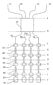
In figure 1 there is shown a tuneable add/drop multiplexer
according to the invention. The support lines A-J illustrate
sections that are used to describe the invention. In the case
of the Figure 1 embodiment, the tuneable add/drop multiplexer
includes four access waveguides 11, 12, 13, 14, one MMI-
waveguide 10, four phase control elements 51, 53, 55 and 57
per Michelson waveguide, three Bragg gratings 62, 64 and 66
Michelson waveguide, and one broadband reflection gratings 70
per Michelson waveguide. One of the Michelson waveguides is
able to manage without a phase control element. The access
waveguides 11, 12, 13 and 14 are arranged on a first side of
the MMI-waveguide. The Michelson waveguides are arranged on a
second side of the MMI-waveguide 10. Arranged in the
CA 02343724 2001-03-08
WO 00/18042 11 PCT/SE99/01496
Michelson waveguides 31, 32, 33 and 34 are said phase control
elements Sl, 53, 55 and 57, the Bragg gra~ings 62, 69 and 66,
and the broadband reflection gratings 70. The broadband
reflection gratings 70 have been placed at the end of the
Michelson waveguidles 31, 32, 33 and 34 in this embodiment.
However, these broadband reflection gratings 70 may
conceivably be arranged at the beginnir_g of said Michelson
waveguides 31, 32, 33 and 34. When the ~roadband reflection
gratings are arranged at the beginning of the Michelson
waveguides, their reflection sections must be provided with
openings (windows) for those channels that shall later be
handled by the Bragg gratings. An example of one such
broadband reflection grating provided with windows is
described in G.P. Agrawal and S. Radic, Phase-shifted Fiber
Gratings and their Application for Wavelength Demultiplexing,
IEEE, Photon. Tech. Lett., Vol. 6(8), pp. 995-997, 1994.
The tuneable add/drop multiplexer according to the Figure 1
embodiment is able to handle three different wavelengths ~.I,
~,2 and ~,3 individually, i.e. each of these wavelengths can be
chosen to be excited out to one of the four access waveguides
I1, 12, 13 and 14 on the first side of t~:e MMI-waveguide 10.
Since this arrangement is primarily conceived for use as a
tuneable add/drop multiplexer, only two c- the four available
access waveguides 11, 12, 13 and 14 will be concerned, partly
that wavelength or those wavelengths to be dropped and partly
those wavelengths or wavelength that will not be dropped. The
wavelength channels that have not been reflected by a Bragg
grating 62, 64 or 66 can be reflected by the broadband
reflection grating 70 arranged at the end of the Michelson
waveguide 31, 32, 33 and 34. Those wavelengths that are
reflected by the broadband reflection gratings 70 can be
chosen to be dropped or not to be dropped with the aid of the
phase control element 57.
CA 02343724 2001-03-08
WO 00/18042 12 PCT/SE99/01496
Of course, the aforesaid tuneable add/drop mult_plexer can be
upgraded to include Q-number of wavelengtz charnels that can
be handled individually, instead of solely three wavelength
channels ~.1, t~2 and ~.3 as in the aforesaid embodiment.
However, in order for the tuneable add/drop multiplexer to be
able to handle Q-number of wavelength channels independently
of one another, it will be necessary for said multiplexer to
include QXN-number of Bragg gratings, (N-1)XQ-number of phase
control elements, N-number of access waveguides arranged on
the first side of the MMI-waveguide, and N-number of
Michelson waveguides arranged on the other side of said MMI-
waveguide in respect of one Nx.N MMI-waveguide.
Assume that light is excited in at the access waveguide 11
belonging to the MMI-waveguide 10 at sect=on A. The length of
the MMI-waveguide 10 is selected so that N-number of images
or reproductions of the light intensity from the access
waveguide 11 at section A is achieved in the MMI-waveguide 10
along section B. Also assume that the structure and
dimensions of the MMI-waveguide IO have been selected so that
four images, i.e. N=4, of the original distribution in the
access waveguide 11 is achieved. Then, if the access
waveguides 11, 12, 13 and 19 have been arranged at the MMI-
waveguide 10 correctly, i.e. have been dimensioned and
positioned correctly, and if the cross-sectional dimensions
and positions of the Michelson waveguides 31, 32, 33 and 34
have been chosen correctly, a large part of the energy in the
images will be coupled to the Michelson waveguides 31, 32, 33
and 34. The maximum energy of these images is <1/N of the
energy along section A if perfect uniformity is achieved, in
this case <1/4 of the energy along section A. Deviation of
this intensity distribution will be very small if light is
excited from one of the access waveguides 12-14 along section .
A instead.
CA 02343724 2001-03-08
WO 00/18042 13 PCT/SE99/01496
Sections along tie support lines D, F and H denote Bragg
grating sections. The Bragg grating sections along respective
support lines may be mutually identical, in which case the
grating sections will reflect respective wavelengths along
respective suppor~ lines for each of the Michelson waveguides
31, 32, 33 and 3=. The wavelengths that are reflected by a
Bragg grating return to the MMI-waveguide 10 with the phase
relationship determined by the phase control elements 51, 53
and 55.
For instance, assume that the Bragg gratings along section D
reflect a wavelength a.l and that the Bragg gratings along
section F reflect a wavelength ?~2. The phase control element
51 along section C will then determine ~r:hich access waveguide
11-14 will be the output port for wavelength ~.1, and the
phase control element 53 along section E will determine which
access waveguide 11-14 will be the output port for wavelength
~.2. The same applies along section G, i.e. respective phase
control element 55 along said section will determine which of
the access waveguides 11-14 will be the output port for the
wavelength ~,3 that has been reflected by the Bragg gratings
along section H.
The phase relationship into the MMI-waveguide 10 in the
reverse direction can thus be chosen individually for each
wavelength. In other words, each wavelength channel can be
given an outport =ndependently of other wavelength channels.
This presumes, of course, that the phase control element 53
along section E, for instance, can comr~ensate for the phase
control element 51 along section C, and that phase control
element 55 along section G can compensate for the phase
control elements 51 and 53 along section C and E
respectively, and that phase control element 57 along section
I can compensate for the phase control elements 51, 53 and 55
along respective sections C, E and G. Generally speaking,
CA 02343724 2001-03-08
WO 00/18042 14 PCT/SE99/01496
each phase contrc_ element shall be able to compensate for
those upstream phase control elements in the transmission
paths of the channels along said Michelson waveguide.
The phase contrcl element 51 along the line C will, of
course, also inf 1 uence the wavelength channels ?_2 and ?~3 .
However, this compensation can be easily controlled with the
aid of software ~:~ accordance with theories that are well
known to the person skilled in this art and that need not
therefore be described in more detail in this document. If it
is not desired to control this compensation with the aid of
software, the phase control elements 51, 53, 55 and 57 can be
successively extended from section C in a direction towards
section I in some suitable way.
The wavelength channel or channels that has/have not been
reflected by a Bragg grating will reach the broadband
reflection gratings 70. When the Michelson waveguides 31, 32,
33 and 34 have equivalent lengths, those wavelength channels
that are reflected by the broadband reflection gratings 70
will be focused on the same access waveguides arranged on the
first side of the MMI-waveguide.
Figure 1 illustrates the principle according to which Q+Y
wavelength channels are handled by a 4X4 MMI-waveguide. Q
channels can be dropped and/or added to a channel stream on
Q+Y channels. The number of channels Q is restricted by the
number of Bragg gratings and phase control elements. Those
wavelength channels Y that are not reflected individually are
reflected in the broadband reflection section and controlled
by forwardly lying phase control elements. Three wavelength
channels can be handled individually in the illustrated case,
whereas the remaining wavelength channels cannot be
controlled individually. Add and drop are both performed in
the same structure in this case. The MMI structure functions
as a splitter from above and down, according to Figure 1, for
CA 02343724 2001-03-08
WO 00/18042 15 PCT/SE99/01496
both transmission channels and add-channels. The channels are
then reflected in respective Bragg grating sections. When the
reflected power again reaches the MMI structure, the relative
phase distribution in the interface between the Michelson
waveguides along section B will determine where the power
will be focused along section A. .wo of the access
waveguides, for instance waveguides 1i and 12, function as
wavelength channel inputs, where one cf said channels is
intended for the add-wavelength channel and the remaining two
access waveguides function as outputs for the wavelength
channels, where one of said channels is intended for the
drop-wavelength channel.
Figure 2 illustrates another embodi:~ent of a tuneable
add/drop multiplexer according to the invention. The support
lines A-H show sections used to describe the invention. This
embodiment includes two MMI-waveguides 10 and 20, six
Michelson waveguides 31, 32, 33, 41, 42 and 43, six access
waveguides 11, 12, 13, 21, 22 and 23, a connecting waveguide
5, an isolator 80, eighteen Bragg gratings 62, 63, 64, 65, 66
and 67, and eighteen phase control elements 51, 52, 53, 54,
55 and 56. Only twelve phase control elements are required in
principle, since one Michelson waveguide per MMI-waveguide
may be without a phase control element.
Three access waveguides 11, 12 and 13 are arranged on the
first side of the MMI-waveguide 10. The Michelson waveguides
31, 32 and 33 are arranged on the opposite side relative to
said access waveguides 11, 12 and 13. Three Bragg gratings
63, 65 and 67 and three phase control elements 52, 54 and 56
are arranged on each of these Michelson waveguides 31, 32 and
33.
Three access waveguides 21, 22 and 23 are arranged on the
first side of the MMI-waveguide 20. The Michelson waveguides
41, 42 and 43 are arranged on the opposite side in relation
CA 02343724 2001-03-08
WO 00/18042 16 PCT/SE99/0149G
to said access waveguides 21, 22 and 23. Three Bragg gratings
62, 64 and 66 and three phase control elements 51, 53 and 55
are arranged on each of these Michelson waveguides 41, 42 and
43.
The access waveguide 13 arranged on the first side of the
first MMI-waveguide 10 is coupled to the access waveguide 21
arranged on the first side of the second MMI-waveguide 20,
via a connecting waveguide 5. This connecting waveguide 5 is
provided with an isolator 80. The tuneable add/drop
multiplexer will also function in the absence of the isolator
80.
Assume that at least one wavelength cannel is sent into an
I5 access waveguide li arranged on the L~~MI-waveguide 10. This
wavelength channel passes through the MMI-waveguide 10. The
length and the structure of the MMI-~aaveguide is chosen so
that N-number of images of the light intensity from the
access waveguide 11 at section A is reached in the MMI-
waveguide along section B. We assume in this case that the
length and the structure have been chosen so as to obtain
three images. If the access waveguides 11, 12 and 13 have
been arranged at the MMI-waveguide 10 correctly, i.e. have
been positioned and dimensioned correctly, and if the cross-
sectional dimensions and positioning of the Michelson
waveguides 31, 32 and 33 have been chosen correctly, a large
part of the energy in the images will be coupled to the
Michelson waveguides 31, 32 and 33. T!:e maximum energy for
these images is <1/N of the energy along section A when
perfect uniformity is achieved, in this case thus <1/3 of the
energy along section A. This intensity distribution will
deviate to a very small extent when light is instead excited
from one of the access waveguides 12 or 13 along section A.
Sections along support lines D, F and H denote Bragg grating
sections. The Bragg gratings 63, 65 and 67 along respective
CA 02343724 2001-03-08
WO 00/18042 17 PC'T/SE99/01496
support lines ma_~ be mutually identical. When the Bragg
gratings are ider.Lical, the grating sections will reflect
respective wavele~gths along respective support lines for
each of the Mich~?son waveguides 31, 32 and 33. Reflected
wavelengths reLU=:: to the MMI-waveguide 10 with the phase
relationship dete~-tined by the phase control elements 52, 54
and 56 respective~y.
Assume, for insta::ce, that the Bragg grating 63 along section
D reflects the wavelength ?~1 and that the Bragg grating 65
along section F re=lects the wavelength ~.2. The phase control
element 52 along section C will then determine which of the
access waveguides 11-13 will be the output port for the
wavelength ~,1, the phase control element 54 along section E
will determine wh-ch of the access waveguides 11-13 will be
the output port fo= the wavelength ~.2. The same applies along
section G, i.e. =sspective phase control elements 56 along
said section will determine which of the access waveguides
11-13 will be the output port for the wavelength ~,3 that has
been reflected by the Bragg grating 67 along section H.
The phase relatio:~ship entering the MMI-waveguide 10 in the
reverse direction can thus be chosen individually for each
wavelength, i.e. each wavelength channel can be given an
output independent of other wavelength channels. This
naturally presumes that, e.g., the phase control element 54
along section E can compensate for the phase control element
52 along section C, and that the phase control element 56
along section G can compensate for the phase control elements
52, 54 along respective sections C and E. In general, each
phase control element shall be able to compensate for the
upstream phase control elements in the channel transmission
paths along the same Michelson waveguide.
Naturally, the phase control element 52 along the support
line C will also influence wavelength channels ~.2 and ~,3.
CA 02343724 2001-03-08
WO 00/18042 18 PCTlSE99/01496
This compensation, however, can be easily controlled with the
aid of software in accordance with theories that are well
known _to the person skilled in this art and that do not
therefore need to be described in more detail here. If it is
not desired to control said compensation with the aid of
software, it is possible to extend the phase control elements
52, 54 and 56 successively from section. C in a direction
towards section G in some suitable way.
The wavelength channel or channels not reflected individually
by a Bragg grating will be excited from respective Michelson
waveguides 31, 32 and 33.
Figure 2 illustrates the principle in which Q wavelength
channels are handled by two 3X3 MMI-waveguides. Three
wavelength channels can be handled individually in this
embodiment. In this case, add and drop are performed in
separate structures. The MMI structures function as a
sp utter f nom the bottom and upwards in accordance with
Figure 2, for both transmission channels and add-channels.
The channels are then reflected in respective Bragg grating
sections. When the reflected power again reaches the first
MMI structure 10 or the second MMI structure 20, the relative
phase distribution in the interface between respective
Michelson waveguides 31, 32, 33 and 41, 42 and 43 along
section B will determine where the power shall be focused
along section A for the first MMI-waveguide 10 and the second
MMI-waveguide 20 respectively. One of the access waveguides,
for instance waveguide 11, functions as a wavelength channel
input while the two remaining access waveguides function as
wavelength channel outputs, where one of said channels is
intended for none or at least one of the drop-wavelength
channels. Access waveguide 13 is coupled to access waveguide
2I via a connecting waveguide 5.
CA 02343724 2001-03-08
WO 00/18042 19 PCT/SE99/01496
The wavelength channel or channels that has or have not been
dropped to the access waveguide 12 is/are transmitted through
said connecting waveguide 5 to the second MMI-waveguide 20.
These wavelength channels pass through the MMI-waveguide 20.
S The length and the structure of the MMI-waveguide 20 are
chosen so that N-number of images of the ?ight intensity from
the access waveguide 21 at section A w>>1 be achieved in the
MMI-waveguide along section B. It is assumed in this case
that the length and the structure have been chosen so as to
obtain three images. If the access waveguides 21, 22 and 23
have been arranged correctly at the M:-lI-waveguide 20, i.e.
have been correctly dimensioned and positioned, and if the
cross-sectional dimensions and positicns of the Michelson
waveguides 41, 42 and 43 have been correctly chosen, a large
part of the energy in the images will be coupled to the
Michelson waveguides 41, 42 and 43. Tne maximum energy for
these images is <1/N of the energy along section A when
perfect uniformity is achieved, in this case thus <1/3 of the
energy along section A. Deviation of this intensity
distribution will be very small when light exits instead from
one of the access waveguides 22 or 23 along section A.
Sections along support lines D, F and ~ denote Bragg grating
sections. The Bragg gratings 62, 64 ar.d 66 along respective
support lines may be mutually identical, in which case the
grating sections will reflect respective wavelengths along
respective support lines for each of the Michelson waveguides
41, 42 and 43. Reflected wavelengths wi~l return to the MMI-
waveguide 20 with the phase relationship determined by the
phase control elements 51, 53 and 55.
Assume, for instance, that the Bragg gratings 62 along
section D reflect the wavelength ~.1, and that the Bragg
gratings 64 along section F reflect the wavelength ~,2. The
phase control element 51 along section C will then determine
which of the access waveguides 21-23 will be the output port
CA 02343724 2001-03-08
WO 00/18042 2 0 PCT/SE99/01496
for wavelength 7~1, and the phase control element 53 along
section E will determine which of the access waveguides 21-23
will _be the output port for the wavelength i_2. The same
applies along section G, i.e. respective phase control
elements 55 along said section will determine ~~rhich of the
access waveguides 21-23 shall be an output port for the
wavelength ~,3 reflected by the Bragg grati;~gs 66 along
section H. In practice, this will be either the access
waveguide 22 or the access waveguide 23, since the access
waveguide 21 of this embodiment is intended for incoming
wavelength channels.
The phase relationship entering the M~~I-:~aveguide 20 in the
reverse direction can thus be selected i::dividually for each
wavelength, that is to say each wavelength channel can be
given an output independent of other wavelength channels.
This naturally assumes that, for instance, the phase control
element 53 along section E can compensate for the phase
control element 51 along section C, and that the phase
control element 55 along section G can compensate for the
phase control elements 51 and 53 along respective sections C
and E. In general, each phase control element shall be able
to compensate for those control elements that are arranged
upstream in the transmission paths of said channels along the
same Michelson waveguide.
The phase control element 51 along the support line C will,
of course, also influence the wavelength channel s ~.2 and ~.3.
This compensation, however, can be read_ly controlled with
the aid of software in accordance with theories that are well
known to the person skilled ~ n this art and tt-~at should not
therefore need to be described in more detail here. When it
is not desired to control said compensation with the aid of '
software, the phase control elements 51, 53 and 55 can be
extended successively from section C in a direction towards
section G in_some suitable way.
CA 02343724 2001-03-08
WO 00/18042 21 PCT/SE99/01496
The wavelength channel or channels that is/are not reflected
by a Bragg gratin~ will be excited from respective Michelson
waveguides 41, 42 end 43.
S
The isolator 80 i~ used to isolate the drop channel from the
add channel. The _::vention illustrated in Figure 2, however,
can function in L::~ absence of an isolator 80. One type of
isolator that can ~e used with the invention is described in
Electronics Letters, 19 June 1996, Vol. 22, No. 13, pp. 711-
713, "Single Mode optical Isolator at I.3 ~.~m using all fibre
components".
Figure 3 illustrates another embodiment of an inventive
tuneable add/drop multiplexer. The support lines A-J show
sections that are used to describe the invention. ~ This
embodiment includes two MMI-waveguides 10 and 20, six
Michelson waveguid~s 31, 32, 33, 41, 42 and 43, six access
waveguides 11, 12, 13, 21, 22 and 23, a connecting waveguide
5, an isolator 80, eighteen Bragg gratings 62, 63, 64, 65, 66
and 67, twenty-four phase control elements 51, 52, 53, 54,
55, 56, 57 and 58, and six broadband reflection gratings 70.
In principle, sixteen phase control elements are sufficient,
since one Michelson waveguide per MMI-waveguide can manage
without a phase control element.
Three access waveguides 11, 12 and 13 are arranged on the
first side of the MMI-waveguide 10. Three Michelson
waveguides 31, 32 and 33 are arranged on the opposite side in
relation to said access waveguides Il, 12 and I3. Three Bragg
gratings 63, 65 and 67, four phase control elements 52, 54,
56 and 58, and one broadband reflection grating 70 are
arranged on each o. said Michelson waveguides 31, 32 and 33.
Three access waveguides 21, 22 and 23 are arranged on the
first side of the MMI-waveguide 20, while three Michelson
CA 02343724 2001-03-08
WO 00/18042 2 2 PCT/SE99/01496
waveguides 4i, 42 and 43 are arranged on the opposite side of
said MMI-waveguide 20 in relation to said access waveguide
21, 22_ and 23. Three Bragg gratings 62, 64 and 66, four phase
control elements 51, 53, 55 and 57, and one broadband
reflection grating 70 are arranged on each of said Michelson
waveguides 41, 42 and 43.
The access wavegu_de 13 arranged on the first side of the
first MMI-waveguide 10 is coupled to the access waveguide 21
on the first side of the second MMI-r~aveguide 20 via a
connecting waveguide 5, said waveguide S being provided with
an isolator 80.
Assume that Gt least one wavelength channel is sent into an
access waveguide 11 arranged on the MMI-waveguide 10. This
wavelength channel passes through the MMI-waveguide. The
length and the structure of the MMI-waveguide 10 is chosen so
that N-number of images of the light intensity from the
access waveguide 11 at section A are obtained in the MMI-
waveguide 10 along section B. We assume in this case that the
length and the structure have been chosen so that three
images will be obtained. If the access waveguides 11, 12 and
I3 have been correctly arranged at the MMI-waveguide 10, i.e.
have been correctly dimensioned and positioned, and if the
cross-sectional dimensions and positioning of the Michelson
waveguides 31, 32 and 33 have been chosen correctly, a large
part of the energy in the images will be coupled to the
Michelson waveguides 31, 32 and 33. The maximum energy for
these images is <1/N of the energy along section A when
perfect uniformity is obtained, in this case thus <1/3 of the
energy along section A. Deviation 'n this intensity
distribution will be very small when light is excited instead
from one of the access waveguides 12 or 13 along section A.
Sections along support lines D, F and H denote Bragg grating
sections. The Bragg gratings along respective support lines
CA 02343724 2001-03-08
WO 00/18042 2 3 PCT/SE99/01496
may be mutually identical, in which case ~he grating sections
will reflect respective wavelengths alone respective support
lines for each of the Michelson waveguides 31, 32 and 33.
Reflected wavelengths return to the MMI-.raveguide 10 with the
phase relationship determined by the phase control elements
52, 54 and 56. Wavelengths that have nor been reflected by a
Bragg grating along the support lines ~, F and H can be
reflected by the broadband reflection gratings 70 along
section J. The phase control element 58 determines on which
access waveguide the wavelengths that have been reflected by
the broadband reflection grating will be =ocused.
Assume, for instance, that the Bragg gratings 63 along
section D reflect the wavelength )~l and that the Bragg
gratings 65 along section F reflect t~:~ wavelength n,2. The
phase control element 52 along section C will then determine
which access waveguide 11-13 will be the output port for the
wavelength ~.1, and the phase control element 54 along section
E will determine which access waveguide 11-13 will be the
output port for the wavelength ~,2. The same applies along
section G, that is to say respective phase control element 56
along said section will determine which access waveguide 11-
13 shall be the output port for the wavelength ~,3 that has
been reflected by the Bragg gratings 67 along section H. In
the illustrated embodiment, this will be either access
waveguide 12 or access waveguide 13 in practice, since access
waveguide 11 is intended for incoming wavelength channels.
The phase relationship within the MMI-waveguide 10 in the
reverse direction can thus be chosen individually for each
wavelength, that is to say each wavelength channel can be
given an output independent of other :ravelength channels.
Naturally, this assumes that, for instance, the phase control
element 54 along section E can compensate for the phase
control element 52 along section C, and that the phase
control element 56 along section G can compensate for the
CA 02343724 2001-03-08
WO 00/18042 2 4 PCT/SE99/01496
phase control eler.~.ents 52 and 54 along respective sections C
and E. Generally, each phase control element shall be capable
of compensating for upstream phase control elements in the
transmission paths of said channels along the same Michelson
waveguide.
The phase control element 52 along the support line C will,
of course, also i~fluence the wavelength channels ~,2 and ~.3.
This compensation. can, however, be readily controlled with
software in accordance with theories well known to the person
skilled in this art and should therefore not need to be
described in more detail here. When ~t is desired not to
control said compensation with the aid of software, the phase
control elements 52, 54, 56 and 58 can be extended
successively from section C towards section G in some
suitable manner.
Figure 3 illustrates the principle in which Q+Y wavelength
channels are handled by two 3X3 MMI-waveguides. Q channels
can be dropped and/or added to a channel stream on Q+Y
channels. The number of channels Q is restricted solely by
the number of separate Bragg gratings and phase control
elements. The Y wavelength channels that are not reflected
individually are reflected in the broadband reflection
section 70 and controlled by the forwardly lying phase
control elements. The illustrated embodiment is able to
handle individually three wavelength channels. In this case,
add and drop are performed in separate structures. The MMI
structures 10 and 20 function as a splitter from below and
upwards in accordance with Figure 3, for both transmission
channels and add-channels. The channels are then reflected in
respective Bragg grating sections. When the reflected power
again reaches the first MMI structure 10 and the second MMI .
structure 20 respectively, the relative phase distribution in
the interface between the Michelson waveguides along section
B will determine where the power will be focused along
CA 02343724 2001-03-08
WO 00/18042 2 5 PCT/SE99/01496
section A for the =first MMI-waveguide 10 and for the second
MMI-waveguide 20. Jne of the access waveguides, for instance
waveguide 11, arra~ged on the MMI-waveguide 10 will function
as a wavelength c::annel input while the remaining two access
waveguides will f~:-~ction as wavelength channel outputs, where
one of these is intended for no or at least one drop-
wavelength channel. Access waveguide 13 is coupled to access
waveguide 21 via G connecting waveguide S.
The wavelength channel or wavelength channels that has/have
not been dropped to the access waveguide 12 is/are
transmitted through said connecting waveguide 5 to the second
MMI-waveguide 20. Said wavelength channel or channels
passes/pass throu;the MMI-waveguide 20. The length and the
structure of the ~~_~!I-waveguide are chosen so that N-number of
images of the ligh~ intensity from the access waveguide 21 at
section A will be obtained in the MMI-waveguide along section
B. We assume in this case that the length and the structure
have been chosen so that three images are obtained. If the
access waveguides 21, 22 and 23 have been correctly arranged
at the MMI-waveguide 20, in other words have been positioned
correctly, and if the cross-sectional dimensions and
positions of the f:ichelson waveguides 91, 42 and 43 have been
chosen correctly, a large part of the energy in the images
will be coupled t~ the Michelson waveguides 41, 42 and 43.
The maximum energy for these images is <1/N of the energy
along section A when perfect uniformity is achieved, in this
case thus <1/3 of the energy along section A. Deviation in
this intensity distribution will be very small when light is
excited instead from either the access waveguide 22 or the
access waveguide 23 along section A.
Sections along support lines D, F and H denote Bragg grating
sections. The Bragg gratings along respective support lines
can be mutually identical, in which case they will reflect
respective wavelengths along respective support lines for
CA 02343724 2001-03-08
WO 00/18042 2 6 PC'T/SE99/01496
each of the Michelson waveguides 41, ~2 and 43. Reflected
wavelengths return to the MMI-waveguide 20 with the phase
relationship determined by the phase control elements 51, 53,
55 and 57.
Assume, for instar:ce, that the Bragg gray=ng 62 along section
D reflects the wavelength ~.1 and that the Bragg grating 64
along section F reelects the wavelength i.2. The phase control
element 51 along section C will then d~~ermine which of the
access waveguides 21-23 will be the cutput port for the
wavelength ~.1, while the phase control element 53 along
section E will determine which of the access waveguides 21-23
will be the output port for the wavelength ~.2. The same
applies along section G, which means that respective phase
control element 55 along said section will determine which of
the access waveguides 21-23 will be the output port for the
wavelength ~,3 that has been reflected by the Bragg grating 65
along section H.
The phase relationship entering the MMI-waveguide 20 in the
reverse direction can thus be chosen individually for each
wavelength, i.e. wavelength channels can be given an output
independent of other wavelength channels. Naturally, this
presumes that, e.g., the phase control element 53 along
section E can compensate for the phase control element 51
along section C, and that the phase control element 55 along
section G can compensate for the phase control elements 51
and 53 along respective sections C and E. Generally, each
phase control element shall be able to compensate for
upstream phase control elements in the transmission path of
the channels along the same Michelson waveguide.
Naturally, the phase control element 51 along the support
line C will also influence the wavelength channels ~.2 and ~.3.
This compensation, however, can be readily controlled with
CA 02343724 2001-03-08
WO 00/18042 2 7 PCT/SE99/01496
software in accordance with theories that are well known to
the person skilled in this art, and should not therefore need
to be described in more detail here. If it is not desired to
control said compensation with the aid of software, the phase
control elements 51, 53, 55 and 57 can be extended
successively from section C in a directio:~ towards section G
in some suitable way.
The wavelength channel or channels that has/have not been
reflected by a Bragg grating can be reflected by the
broadband reflection grating 70 arranged at the end of the
Michelson waveguides 41, 42 and 43. The broadband reflection
gratings can conceivably be arranged a~ the beginning of the
Michelson waveguides 31, 32, 33, 41, -~_2 and 43. However, the
broadband reflection sections must then have openings
(windows) for those channels that shall be handled by the
Bragg grating sections. An example o~ one such broadband
reflection grating provided with openings is described in
G.P. Agrawal and S. Radio, Phase=shifted Fiber Gratings and
their Application for Wavelength Demultiplexing, IEEE Photon.
Tech. Lett., Vol. 6(8), pp. 995-997, 1994.
The isolator 80 is used to isolate the drop channel from the
add channel. The invention illustrated in Figure 3 can,
however, function in the absence of an isolator 80. One type
of isolator that can be used in the invention is described in
Electronics Letters, 19 June 1996, Vol. 22, No. 13, pp. 711-
713, "Single Mode optical Isolator at 1.3 ~m using all fibre
components".
Figure 4 illustrates a further embodiment of an inventive,
tuneable add/drop multiplexer. The s~:pport lines A-Q show
sections that are used to describe the invention. This
embodiment includes two MMI-waveguides 10 and 20, three
Michelson waveguides 31, 32 and 33, six access waveguides 11,
12, 13, 21, 22 and 23, one connecting waveguide 5, eighteen
Bragg gratings 63, 65 and 67, and t~.renty-one phase control
CA 02343724 2001-03-08
WO 00/18042 2 8 PCT/SE99/01496
elements 52, 54, ~o' and 58. Fourteen phase control elements
will suffice in p=inciple, since one Michelson waveguide can
manage without phase control elements.
Three access wave.~uides 11, 12 and 13 are arranged on the
first side of tie MMI-waveguide 10 and three Michelson
waveguides 31, 32 and 33 are arranged on the opposite side of
said MMI-waveguid~ in relation to said access waveguides. Six
Bragg gratings 63, 65 and 67 and seven phase control elements
52, 54, 56 and 58 are arranged on each of these Michelson
waveguides 41, 32 and 33.
Three access waveguides 21, 22 and 23 are arranged on the
first side of the :~IMI-waveguide 20. The Michelson waveguides
31, 32 and 33 including said Bragg gratings 63, 05 and 67 and
said phase contro~ elements 52, 54, 56 and 58 are arranged on
said Michelson waveguides 31, 32 and 33 on the opposite side
of said MMI-waveguide 20 in relation to said access
waveguides.
The access waveguide 13 arranged on the first side of the
first MMI-waveguide 10 is coupled to the access waveguide 23
on the first side of the second MMI-waveguide via a
connecting waveguide 5.
In the Figure 4 embodiment, the Bragg grating sections D, F
and H and the phase control sections C, E and G are mirror
images around section I of the Bragg grating sections N, L
and J and the phase control sections 0, M and K. It is also
conceivable that the phase control sections and Bragg grating
sections respectively are not in the same order as seen from
the two MMI-waveguides up to the phase control section I,
i.e. when the Bragg grating section C reflects a wavelength
~,1, the Bragg grating section N, for instance, can reflect
either the wavelength 7~2 or the wavelength ~,3. If the Bragg
grating section F reflects a wavelength ~.2, the Bragg grating
CA 02343724 2001-03-08
WO 00/I8042 2 g PCT/SE99/01496
section L can reflect a wavelength ~1 or ~3, and when the
Bragg grating section H reflects a wavelength ~.3, the Bragg
grating section J can reflect a wavelength ~,1 or ~.2.
Assume that a wavelength channel is sent into the access
waveguide 11 on t::e MMI-waveguide 10. This wavelength channel
passes through t~e MMI-waveguide 10. The length and the
structure of the I~_'~!I-waveguide 10 are chosen so that N-number
of images of the i'_ght intensity from the access waveguide 11
at section A will be obtained in the MMI-waveguide 10 along
section B. We assume in this case that the length and the
structure have been chosen so as to obtain three images. If
the access wavegLides 11, 12 and 13 have been correctly
arranged at the _~=~~I-waveguide 10, i.e. have been correctly
I5 dimensioned and positioned, and if the cross-sectional
dimensions and positions of the Michelson waveguides 31, 32
and 33 have been chosen correctly, a large part of the energy
in the images will be coupled to the Michelson waveguides 31,
32 and 33. The maximum energy for these images is <1/N of the
energy along section A when perfect uniformity is obtained,
in this case thus <1/3 of the energy along section A.
Deviation in this intensity distribution will be very small
when light is excited instead from one of the access
waveguides 12 or 13 along section A.
Sections along support lines D, F, H, J, L and N denote Bragg
grating sections. The Bragg gratings along respective support
lines may be mutually identical, in which case the grating
sections will reflect respective wavelengths along respective
support lines for each of the Michelson waveguides 31, 32 and
33. Wavelengths that arrive from the MMI-waveguide 10 and are
reflected by the Bragg gratings 63, 65 and 67 along
respective sections D, F and H return to the MMI-waveguide 10
with the phase relationship determined by the phase control
elements 52, 54 and 56 along respective sections C, E and G.
The wavelengths arriving from the MMI-waveguide 20 and
CA 02343724 2001-03-08
WO 00/18042 30 PCT/SE99/01496
reflected by the Bragg gratings 63, 65 and 67 along
respective sections N, L and J return to the MMI-waveguide 20
with the phase relationship determined by the phase control
elements 52, 54 and 56 along respective sections O, M and K.
Transmitting wavelengths that are not reflected by Bragg
gratings 63, 65 or 67 are controlled ~-_~ the phase control
element 58 along section I in respect of wavelengths that
arrive both from the MMI-waveguide 10 and the MMI-waveguide
20.
Assume, for instance, that the Bragg gratings along sections
D and N reflect the wavelength ~.l and that the Bragg gratings
along sections F and L reflect the wavel ength ~,2. The phase
control element 52 along respective sections C and O will
then determine which of the waveguides 11-13 and 21-23
respectively will be the output port for the wavelength ~,1,
while the phase control elements 54 along respective sections
E and M will determine which of the access waveguides 11-13
and 21-23 respectively will be the output port for the
wavelength ~.2. The same applies along sections G and K, i.e.
respective phase control elements 56 along said sections will
determine which of the respective waveguides 11-13 and 21-23
will be the output port for the wavelength ~.3 that has been
reflected by the Bragg gratings along sections H and J.
The phase relationship entering the MMT_-~~~aveguides 10 and 20
in the reverse direction can thus be c~osen individually for
each wavelength, i.e. each wavelength channel can be given an
output independent of other wavelength channels. This
presumes, of course, that, e.g., the phase control element 54
along respective sections E and M cn compensate for the
phase control element 52 along respective sections C and O,
and that the phase control element 56 along respective
sections G and K can compensate for the phase control
elements 52 and 54 along sections C and E and along sections
CA 02343724 2001-03-08
WO 00/18042 31 PCT/SE99/01496
O and M respectively. Generally, each phase control element
shall be able to compensate for upstream phase control
elements in the transmission paths of the channels along the
same Michelson waveguide.
Naturally, the phase. control element 52 along respective
support lines C and O will also influence the wavelength
channels ~,2 and ~.3. This compensation, however, can be
readily controlled with software in accordance with theories
IO well known to the person skilled in ti:is art and should not
therefore need to be described in more detail here. If it is
not desired to control said compensation with software, the
phase control elements 52, 54 and 56 can be extended from
section C in a direction towards secticn R and from section O
in a direction towards section K respectively, in some
suitable manner.
Figure 4 illustrates the principle in which Q+Y wavelength
channels are handled by two 3X3 and MMI-waveguides. Q
channels can be dropped and/or added separately to a channel
stream on Q+Y channels. The number of channels Q+Y is
restricted solely by the bandwidth of the MMI-waveguides 10
and 20. The number of channels Q is res~ricted by the number
of Bragg gratings 63, 64 and 67 and phase control sections
52, 54 and 56. The non-reflected wavelength channels Y are
transmitted from the access waveguide 11 through the MMIMZI
structure and controlled to the access waveguide 21 with the
phase control section I between tha mutually identical
reflection sections D-H and N-J respectively. Three
wavelength channels can be handled individually in the
illustrated embodiment.
The wavelength channel or channels that has/have not been
dropped to the access waveguide 12, is/are transmitted
through said connecting waveguide ~ to the second MMI-
waveguide 20. These wavelength channels pass through the MMI-
CA 02343724 2001-03-08
W O 00/ 18042 3 2 PCT/S E99/01496
waveguide 20. Ti:e length and the structure of the MMI-
waveguide are chosen so that N-number of images of light
intensity from the access waveguide 23 at section Q will be
obtained in the M:-!=-waveguide along section P. We assume in
this case that the length and the structure is chosen so that
three images are obtained. If the access waveguides 21, 22
and 23 have been G=ranged correctly at the MMI-waveguide 20,
i.e. have been ..orrectly positioned, and if the cross-
sectional dimens_ons and positions of the Michelson
waveguides 31, 32 and 33 have been correctly chosen, a large
part of the energy in the images will be coupled to the
Michelson waveguides 31, 32 and 33. The maximum energy for
these images is <1/N of the energy along section K when
perfect uniformity .s achieved, in this case thus <1/3 of the
energy along section K. Deviation of this intensity
distribution will be very small when light is excited instead
from one of the access waveguides 21 or 22 along section Q.
Sections along support lines N, L and J denote Bragg grating
sections. The Bragg gratings along respective support lines
may be mutually identical, in which case the grating sections
will reflect respective wavelengths along respective support
lines for each oz the Michelson waveguides 3i, 32 and 33.
Reflected wavelengths return to the MMI-waveguide 20 with the
phase relationship determined by the phase control elements
52, 54 and 56.
Assume, for instance, that the Bragg gratings along section J
reflect the wavelength a.3, and that the Bragg gratings along
section L reflect the wavelength i.2. The phase control
element 56 along section K will then determine which access
waveguide 21-23 will be the output port for the wavelength
~.3, and the phase control element 5~ along section M will
determine which access waveguide 21-23 will be the output
port for the wavelength ~.2. The same applies along section O,
i.e. respective phase control element 52 along said section
CA 02343724 2001-03-08
WO 00/18042 3 3 PCT/SE99/01496
will determine which access waveguide 21-23 will be the
output port for the wavelength t~l, which has been reflected
by the, Bragg gratings along section N.
The phase relationship entering the MMI-:aaveguide 20 in the
reverse direction can thus be c~osen i::dividually for each
wavelength, i.e. each wavelength channel can be given an
output independent of other wavelength channels. This, of
course, presumes shat, a g, the phase control element 54
along section M can compensate for the phase control element
52 along section 0, and that the phase control element 56
along section K can compensate for the phase control elements
52 and 54 along respective sections 0 and M. Generally, each
phase control element shall be able Lo compensate for
upstream phase control elements in the t=ansmission paths of
the channels along the same Michelson waveguide.
The wavelength channel or channels that are excited into the
access waveguide 11 and not reflected by a Bragg grating are
led to the access waveguide 21 arranged on the first side of
the second MMI-waveguide 20.
Figure 5 illustrates yet another embodiment of an inventive
tuneable add/drop multiplexer. The support lines A-Q show
sections used to describe the invention. This embodiment
includes four MMI-waveguides 10, 20, 30 and 40, six Michelson
waveguides 31, 32, 33, 34, 35 and 36, twelve access
waveguides 11, 12, 13, 21, 22, 23, 37, 38, 39, 41, 42 and 43,
three connecting waveguides 5, 6 and 7, thirty-six Bragg
gratings 62, 63, 64, 65, 66 and 67, and forty-two phase
control elements 51, 52, 53, 59, 55, 56, 57 and 58. Twenty-
eight phase control elements will suffice in principle, since
one of the Michelson waveguides 31, 32 or 33 and one of the
Michelson waveguides 34, 35 or 36 are able to manage
completely without phase control elements.
CA 02343724 2001-03-08
WO 00/18042 3 4 PCT/SE99/01496
Three access waveguides 11, 12 and 13 are arranged on the
first side of a first MMI-waveguide 10, wzile three Michelson
waveguides 31, 32 and 33 are arranged on the other side
relative to said access waveguides. Six Bragg gratings 63,
65, 67 and seven phase control elements 52, 54, 56 and 58 are
arranged on each of these Michelson wavew::ides 31, 32 and 33.
Three access waveguides 21, 22 and 23 Gre arranged on the
first side of a second MMI-waveguide 20, :~,hile said Michelson
waveguides 31, 32 and 33 that include said six Bragg gratings
63, 65, 67 and said seven phase control dements 52, 54, 56
and 58 are arranged on the opposite side relative to said
access waveguides.
The access waveguide 11 arranged on the first side of the
first MMI-waveguide 10 is coupled to the access waveguide 21
on the first side of the second NI!~I-waveguide via a
connecting waveguide 7.
Three access waveguides 37, 38 and 39 are arranged on the
first side of a third MMI-waveguide, Gnd three Michelson
waveguides 34, 35 and 36 are arranged c:~ the opposite side
relative to said access waveguides. Arranged on each of these
Michelson waveguides 34, 35 and 36 are six Bragg gratings 62,
64, 66 and seven phase control elements 5., 53, 55 and 59.
Three access waveguides 41, 42 and 43 are arranged on the
first side of a fourth MMI-waveguide 40, ;rhile said Michelson
waveguides 34, 35 and 36 that include said six Bragg gratings
62, 64, 66 and said seven phase control elements 51, 53, 55
and 59 are arranged on the opposite side relative to said
access waveguides 41, 42 and 43.
A third access waveguide 23 arranged on the first side of the
second MMI-waveguide 20 is coupled to a first access
waveguide 37 arranged on the first side of the third MMI-
CA 02343724 2001-03-08
WO 00/18042 3 5 PCT/SE99/01496
waveguide, via a connecting waveguid~ 6. A third access
waveguide 39 arranged on the first side of the third MMI
waveguide 30 is coupled to a third access waveguide 43
arranged on the first side of the fourth MMI-waveguide 40,
via a connecting waveguide 5.
In the Figure 5 embodiment, the Bragg gratings 63, 65 and 67
and the phase control elements 52, 54 and 56 along respective
sections D, F and H and C, E and G are a mirror image around
section I of the Bragg gratings 52, 54 and 56 and phase
control elements 63, 65 and 67 along respective sections N, L
and J and O, M and K. In other words, the Bragg gratings 63
reflect a wavelength ~,1, the Bragg Gratings 65 reflect a
wavelength )~2, and the Bragg gratings 67 reflect a wavelength
~.3. It is conceivable that the Bragg gratings along the
sections D and N, F and L, and H and ~ respectively will not
reflect the same wavelengths. If the Bragg gratings 63 along
section D reflect a wavelength ~,1, the Bragg gratings 63
along section N may reflect a wavelength ~,2 or ~.3. If the
Bragg gratings 65 along section F reflect a wavelength ~.2,
the Bragg gratings 65 along section L may reflect a
wavelength ~.1 or ~,3, and if the Bragg gratings 67 along
section H reflect a wavelength ~.3, ~~e Bragg gratings 67
along section J may reflect a wavelength ~.1 or ~.2.
In the Figure 5 embodiment, the Bragg Gratings 62, 64 and 66
and the phase control elements 5I, 53 and 55 along respective
sections D, F, H and C, E, G are a mirror image around
section I of the Bragg gratings 62, 6~ and 66 and the phase
control elements 51, 53 and 55 along respective section N, L,
J and O, M, K. In other words, the Brag gratings 62 reflect
a wavelength ~.9, the Bragg gratings 64 reflect a wavelength
~.5, and the Bragg gratings 66 reflect a wavelength ~.6.
Conceivably, the Bragg gratings along respective sections D
and N, F end L, H and J will nom reflect the same
CA 02343724 2001-03-08
WO OO/I8042 3 6 PCT/SE99/01496
wavelengths. If tc:~ Bragg gratings 62 along section D reflect
a wavelength ~.4, ~.he Bragg gratings 62 along section N may
reflect a wavelenc~h ~,5 or ~.6. If the Bragg gratings 64 along
section F reflec~ a wavelength ~,5, the Bragg gratings 64
along section L may reflect a wavelength ~,4 or ~.6, while if
the Bragg gratin~s 66 along section H reflect a wavelength
~,6, the Bragg gratings 66 along section J may reflect a
wavelength ~.4 or i.5.
The Bragg gratings 63, 65 and 67 preferably reflect other
wavelengths than she Bragg gratings 62, 64 and 66, in other
words when the B=agg gratings 63, 65 and 67 reflect the
wavelengths n.l-?", :.he Bragg gratings 62, 64 and 66 will
reflect the wavelengths ~.4-~.6.
The phase contrc~ elements 58 and 59 can control those
wavelengths that are not reflected individually by a Bragg
grating.
Assume that at least one wavelength channel is excited into
the access waveguide 13 arranged on the MMI-waveguide 10.
This wavelength c::annel passes through the MMI-waveguide 10.
The length and tie structure of the MMI-waveguide 10 are
chosen so as to obtain N-number of images of the light
intensity from the access waveguide 13 at section A in the
MMI-waveguide 10 along section B. We assume in this case that
the length and s;.ructure have been chosen so as to obtain
three images. If the access waveguides 11, 12 and 13 have
been arranged correctly at the MMI-waveguide 10, i.e. have
been correctly positioned and dimensioned, and if the cross-
section dimensions and positions of the Michelson waveguides
31, 32 and 33 have been correctly chosen, a large part of the
energy in the images will be coupled to the Michelson
waveguides 31, 32 and 33. The maximum energy for these images
is <1/N of the energy along section A if perfect uniformity
CA 02343724 2001-03-08
WO 00/18042 3 7 PCT/SE99/0149b
is achieved, in this case thus <1/3 of the energy along
section A. Deviation of this intensity distribution will be
very slight when she light is excited? instead from one of
the access waveguides 11 or 12 along section A.
Sections along support. lines D, F and H denote Bragg grating
sections. The Bragg gratings 63, 65 and 67 along said support
lines may be mutually identical, in which case said grating
sections will reflect respective wavelengths that arrive from
the MMI-waveguide 10 along respective support lines for each
of the Michelson waveguides 31, 32 and 33. Reflected
wavelengths return to the MMI-waveguide 10 with the phase
relationship deter~~ined by the phase control elements 52, 54
and 56.
Assume, for instance, that the Bragg grating 63 along section
D reflects the wavelength ?~I, and the Bragg grating 65 along
section F reflects the wavelength ~.2. The phase control
elements 52 along section C will then determine which access
waveguide 11-13 will be the output port for the wavelength
~,1, and the phase control elements 54 along section E will
determine which access waveguide 11-13 will be the output
port for the wavelength ~,2. The same applies along section G,
i.e. respective phase control elements 56 along said section
determine which of the access waveguides 11-13 shall be the
output port for the wavelength ?.3 that has been reflected by
the Bragg gratings 67 along section H.
The phase relationship entering the MMI-:~~aveguide 10 in the
reverse direction can thus be chosen individually for each
wavelength, in other words each wavelength channel can be
given an output independent of other wavelength channels.
This naturally assumes that, e.g., the phase control element
54 along section E can compensate for the phase control
element 52 along section C, and that the phase control
CA 02343724 2001-03-08
WO 00/18042 3 g PCT/SE99/OI496
element 56 along section G can compensate for the phase
control elements 52 and 54 along respective sections C and E.
Generally, each phase control elemen~ shall be able to
compensate for upstream phase control elements in the
transmission paths of the channels along the same Micheison
waveguide.
Naturally, the phase control element ~2 along the support
line C will also influence the wavelength channels ~,2 and ?~3.
This compensation, however, can be readily controlled with
software in accordance with theories tt-:at are well known to
one skilled in this art and should not therefore need to be
described in more detail here. If i:. is not desired to
control said compensation with the aid cT software, the phase
control elements 52, 54 and 56 can be er.~ended successively
from section C towards section G in some suitable way.
The access waveguide 11 is coupled to the access waveguide 21
via the connecting waveguide 7. The wavelength channel or
channels that has/have been reflected and not dropped to the
access waveguide 12 is/are transmitted out through the access
waveguide 11 and through said connecti~g waveguide 7 to the
access waveguide 21 arranged on the seconc MMI-waveguide 20.
These wavelength channels pass through she MMI-waveguide 20.
The length and structure of the MMI-waveguide have been
chosen so as to obtain in the MMI-waveguide along section P
N-number of images of the light intensity from the access
waveguide 21 at section Q. We assume =~ this case that the
length and structure have been chosen so as to obtain three
images. If the access waveguides 21, 22 and 23 have been
correctly arranged at the M~:I-waveguice 20, i.e. correctly
positioned and dimensioned, and if the cross-sectional
dimensions and positions of the Michelson waveguides 31, 32
and 33 have been chosen correctly, a large part of the energy
in the images will be coupled to the Michelson waveguide 31,
32 and 33. The maximum energy for these images is <1/N of the
CA 02343724 2001-03-08
WO 00/18042 3 g PCT/SE99/01496
energy along section Q if perfect uniformity is achieved, in
this case thus <1/3 of the energy along section Q. Deviation
of this intensity distribution will be very small when light
is instead excited,from one of the access waveguides 22 or 23
along section Q.
Sections along support lines N, L and J denote Bragg grating
sections. Bragg gratings 63, 65 and 67 along respective
support lines may be mutually identical, in which case the
grating sections will reflect respective wavelengths along
respective support lines for each of the Michelson waveguides
31, 32 and 33. Reflected wavelengths will return to the MMI-
waveguide 20 with the phase relationship determined by the
phase control elements 52, 54 and 56.
Assume, for instance, that the Bragg gratings 63 along
section N reflect the wavelength ~,1 and that the Bragg
gratings 65 along section L reflect the wavelength ~.2. The
phase control elements 52 along section O will then determine
which access waveguide 21-23 will be the output port for the
wavelength ~.1, and the phase control element 54 along section
M will determine which access waveguide 21-23 will be the
output port for the wavelength ~.2. The same applies along
section K, in other words respective phase control element 56
along said section determine which access waveguide 21-23
will be the output port for the wavelength ~,3 that has been
reflected by the Bragg gratings along section J.
The phase relationship entering the M:~I-waveguid~ 20 in the
reverse direction can thus be selected individually for each
wavelength, which means that each wavelength channel can be
given an output independent of other wavelength channels.
This naturally presumes that, e.g., the phase control element
54 along section M can compensate for the phase control
element 52 along section O, and that the phase control
CA 02343724 2001-03-08
WO 00/18042 4 0 PC1'/SE99/01496
element 56 along section K can compensate for the phase
control elements ~~ and 54 along respective sections O and M.
Generally, each ~zase control element shall be able to
compensate for ti:e upstream phase control elements in the
transmission pathslalong the same Michelson waveguide.
Naturally, the p:.ase control element 52 along the support
line O will also _~:fluence the wavelength channels ~.2 and ),,3.
This compensation, however, can be readily controlled by
software in accordance with theories that are well known to
the person skilled in this art and should not therefore need
to be described in more detail here. If it is not desired to
control said compe~sation with the aid of software, the phase
control elements ~2, 54 and 56 can be extended successively
from section O i:: a direction towards section K in some
suitable manner.
The wavelength channel or channels that has/have been excited
into the access waveguide 13 and has/have not been reflected
by a Bragg grating will be focused with the aid of the phase
control element 58 along section I on the access waveguide 23
arranged on the f~.rst side of the second MMI-waveguide 20.
These wavelengths Together with those wavelengths that have
been transmitted trough the connecting waveguide 7, plus the
add-wavelength channels that have been excited into the
access waveguide 22 and which have also been reflected by a
Bragg grating 63, 65 or 66 along sections N, L and J arranged
in the Michelson waveguides 31, 32 and 33, will be focused to
the access waveguide 23 arranged on the first side of the
second MMI-waveguide 20. The access waveguide 23 is connected
with the access waveguide 37 via the connecting waveguide 6.
Said wavelength channels are excited into the first access
waveguide 37 arranged on the third MMI-~aaveguide 30.
These wavelength channels pass through the MMI-waveguide 30.
The length and the structure of the MMI-waveguide 30 are
CA 02343724 2001-03-08
WO 00/18042 41 PCT/SE99/01496
chosen so that N-number of images of the light intensity from
the access waveguide 37 at section Q will be obtained in the
MMI-waveguide 30 along section P. we assume in this case that
the length and structure have been chosen so as to obtain
three images. If the access waveguides 37, 38 and 39 have
been correctly arranged at the MMI-waveguide 30, i.e. have
been correctly positioned and dimensioned, and if the cross-
sectional dimens_ons and positions of the Michelson
waveguides 34, 35 and 36 have been correctly chosen, a large
part of the energy in the images will be coupled to the
Michelson waveguides 34, 35 and 36. The maximum energy for
these images is <1/N of the energy along section Q if perfect
uniformity is achieved, in this case thus <1/3 of the energy
along section Q. deviation of this intensity distribution
will be very small, if light is, instead, excited from one of
the access waveguides 38 or 39 along section Q.
Sections along support lines N, L and J denote Bragg grating
sections. The Bragg gratings 62, 64 and 66 along respective
support lines may be mutually identical, in which case the
grating sections will reflect respective wavelengths along
respective support lines for each of the Michelson waveguides
34, 35 and 36. Reflected wavelengths will return to the MMI-
waveguide 30 with the phase relationship determined by the
phase control elements 51, 53 and 55.
Assume, for instance, that the Bragg gratings along section N
reflect the wavelength ~.9 and that the Bragg gratings along
section L reflect the wavelength ~,5. The phase control
element 51 along section O will then determine which access
waveguide 37-39 will be the output port for the wavelength
~,4, while the phase control element 53 along section M will
determine which access waveguide 37-39 will be the output
port for the wavelength ~,5. The same applies along section K,
i.e. respective phase control element 55 along said section
will determine which of the access waveguides 37-39 shall be
CA 02343724 2001-03-08
WO 00/18042 4 2 PCT/SE99/01496
the output port of the wavelength ~.6 tt-_a~ has been reflected
by the Bragg gratings along section J.
The phase relationship entering the MhIT-:~~aveguide 30 in the
reverse direction can thus be selected _:.dividually for each
wavelength. In other words, each wave~ength channel can be
given an output independent of other ~;avelength channels.
This naturally presumes that, e.g., the chase control element
53 along section M can compensate for the phase control
element 51 along section C, and that the phase control
element 55 along section K can compensate for the phase
control elements 51, 53 along respecti~~e sections O and M.
Generally, each phase control elemen= shall be able to
compensate for the upstream phase con~rol elements in the
transmission paths of the channels along the same Michelson
waveguide.
Naturally, the phase control element 51 along the support
line O will also influence the wavelength channels ~.5 and ~,6.
However, this compensation can be readily controlled with the
aid of software in accordance with theories that are well
known to the skilled person in this field, and that should
therefore not need to be described in mc=a detail here. If it
is not desired to control this compensa~ion with the aid of
software, the phase control elements 51, 53 and 55 can be
extended successively from section O it a direction towards
section K, in a suitable manner.
The wavelength channel or channels that has/have been
reflected and not dropped to the access waveguide 38 are
transmitted out from the access wavegu=de 39 arranged on a
third MMI-waveguide and pass through said connecting
waveguide 5 to the access waveguide ~3 on the fourth MMI-
waveguide 40. These wavelength channels pass through the MMI-
waveguide 40. The length and structure of the MMI-waveguide
have been__chosen so as to obtain N-number of images of the
CA 02343724 2001-03-08
WO 00/18042 4 3 PCT/SE99/01496
light intensity frem the access waveguide 43 at section A in
the MMI-waveguide along section B. We assume in this case
that the length Gnd structure have been chosen so as to
obtain three images. If the access waveguides 41, 42 and 43
have been correctly arranged at the MMI-waveguide 40, i.e.
correctly positioned and dimensioned, and if the cross-
sectional dimensions and positions of the Michelson
waveguides 34, 35 and 36 have been correctly chosen, a large
part of the energy in the images will be coupled to the
Michelson waveguides 34, 35 and 36. The maximum energy for
these images is <1/N of the energy along section B if perfect
uniformity is achieved, in this case thus <1/3 of the energy
along section A. Deviation of this intensity distribution
will be very small, if light is instead excited? from one of
the access waveguides 41 or 42 along section A.
Sections along support lines D, F and H denote Bragg grating
' sections . The Bragg gratings 62, 64 and 66 along respective
support lines may be mutually identical, in which case the
grating sections reflect respective wavelengths along
respective support lines for each of the Michelson waveguides
34, 35 and 36. Reflected wavelengths return to the MMI
waveguide 40 with the phase relations::ip determined by the
phase control elements 51, 53 and 55.
Assume, for instance, that the Bragg gratings along section D
reflect the wavelength 7~4, and that the Bragg gratings along
section F reflect the wavelength ~.5. The phase control
elements 51 along section C will then determine which of the
access waveguides 41-43 will be the output port for the
wavelength ~.4, and the phase control element 53 along section
E will determine which of the access waveguides 41-43 will be
the output port for the wavelength 7~5. The same applies along
section G, in other words respective phase control elements
55 along said section will determine which of the access
waveguides 41-43 will be the output port for the wavelength
CA 02343724 2001-03-08
WO 00/18042 4 4 PCT/SE99/01496
~.6 that has beer. reflected by the Bragg grating 66 along
section H.
The phase relatic:a hip entering the MMI-waveguide 40 in the
S reverse direction can thus be chosen individually for each
wavelength. In o~~:er words, each wavelength channel can be
given an output _zdependent of other wavelength channels.
Naturally, this presumes that, e.g., the phase control
element 53 along section E can compensate for the phase
control element ~- along section C, and that the phase
control element ~.. along section G can compensate for the
phase control eler~:ents 51, 53 along respective sections C and
E. Generally, eac~ phase control element shall be able to
compensate for t~~ upstream phase control elements in the
transmission path= of the channels along the same Michelson
waveguide.
The phase control element 51 along the support line C will,
of course, also i::fluence the wavelength channels ~.5 and ~,6.
This compensation, however, can be readily controlled with
software in accordance with theories which are well known to
the person skilled in this art and which therefore need not
be described in d~~ail here. If it is not desired to control
said compensation ::ith the aid of software, the phase control
elements 51, 53 and 55 can be extended successively from
section C in a di=ection towards section G in some suitable
manner.
Figure 6 illustrates another embodiment of an inventive
tuneable add/drop multiplexer. The support lines A-P show
sections that are used to describe the invention. This
embodiment includes two MMI-waveguides 10 and 20, six
Michelson waveguides 31, 32, 33, 41, 42 and 43, six access '
waveguides 11, 12, 13, 21, 22 and 23, a connecting waveguide
5, an isolator 80, six 1XN switches 110, 111, 112, 113, 114
CA 02343724 2001-03-08
WO 00/18042 4 5 PCT/SE99/01496
and 115 and six reflection sections 120, 121, 122, 123, 124
and 125.
Three access waveg,uides 11, 12 and 13 are arranged on the
first side of the MMI-waveguide 10, while three Michelson
waveguides 31, 32 and 33 are arranged on the opposite side in
relation to said access waveguides 11, 12 and 13. A 1XN
switch 110, 112 and 114 and a reflection section 120, 112 and
124 are arranged on each of said Michelson waveguides 31, 32
and 33.
Three access waveguides 21, 22 and 23 are arranged on the
first side of the MMI-waveguide 20, while three Michelson
waveguides 41, 42 and 43 are arranged on r.he opposite side in
relation to said access waveguides 21, 22 and 23. A 1XN
switch 111, 113 and 115 and a reflection section 121, 123 and
125 are arranged respectively on each of the Michelson
waveguides 41, 42 and 43.
The access waveguide 13 arranged on the first side of the
first MMI-waveguide 10 is coupled to the access waveguide 21
on the first side of the second MMI-waveguide 20 via a
connecting waveguide 5. This connecting waveguide 5 is
provided with an isolator 80.
Assume that at least one wavelength channel is sent into an
access waveguide 11 arranged on the MMI-waveguide 10. This
wavelength channel passes through the MMI-waveguide. The
length and the structure of the MMI-waveguide 10 are chosen
so as to obtain N-number of images of the light intensity
from the access waveguide 11 at section A in the MMI-
waveguide 10 along section B. We assume in this case that the
length and the structure have been chosen so as to obtain
three images. If the access waveguides 11, 12 and 13 have
been correctly arranged at the MMI-waveguide 10, i.e. have
been correctly dimensioned and positioned, and if the cross-
CA 02343724 2001-03-08
WO 00/18042 4 6 PCT/SE99/01496
sectional dimensions and positions of the Micheison
waveguides 31, 32 and 33 have been chosen correctly, a large
part -of the energy in the images will be coupled to the
Michelson waveguides 31, 32 and 33. T~:e maximum energy for
these waveguides ,is <1/N of the enerc_; along section A if
perfect uniformity is achieved, in this case thus <1/3 of the
energy along section A. Deviation in this intensity
distribution will be very small if ligh~ is, instead, excited
from one of the access waveguides 12 or 13 along section A.
Figure 7 illustrates a suitable 1XN switch for use with the
inventive embodiment according to Figure 6. The 1XN switch
shown in Figure 7 is an MMIMZI-based switch (Multi Mode
Interference Mach-Zehnder Interferometer). Any 1XN switch
whatsoever will be suitable in principle, providing that a
reciprocal behaviour exists. A reciprocal 1XN switch is a
switch that does not include a reciprocal element. A
reciprocal behaviour means that light =ollows the same path
through an element with the same _osses regardless of
direction.
The 1XN switch, where N=4, in Figure 7, includes one 1XN MMI-
waveguide 240, where N=4, four Mach-Ze~nder waveguides 45,
46, 47 and 48, four phase control eleme~as 201, 203, 205 and
207, and one NXN MMI-waveguide 230, where N=4. Arranged on a
first side of the 1X4 MMI-waveguide is, for instance, the
Michelson waveguide 31. The aforesaid Mach-Zehnder waveguides
45, 46, 47 and 48 including respective :base control elements
201, 203, 205 and 207 are arranged on .. second side of said
one 4X4 MMI-waveguide. The Mach-Zehnde~ waveguides are also
arranged on a first side of said 4X4 M:~:=-waveguide 230. Four -
Michelson waveguides 91, 92, 93 and := are arranged on a
second side of said 4X4 MMI-waveguide. Three phase control -
elements will suffice in principle, s_nce one Mach-Zehnder
waveguide may be without a phase contro_ element.
CA 02343724 2001-03-08
WO 00/18042 4 7 PCT/SE99/01496
The wavelength ci:annels excited out in one of the Michelson
waveguides 31, 32 and 33 on the MMI-waveguide 10 first pass
slightly therethrough and are thereafter transmitted through
the aforesaid lXN,switch. This switch causes the wavelength
channels to exit Through one of its N-outputs.
Assume that 1XN s:~:itches 110, 112 and 114 are set so that the
wavelength channels will be excited to the Michelson
waveguide 31.
As before mentioned, the Michelson waveguides 91, 92, 93 and
94 belonging to the 1XN switches 110, 112 and 119 are
provided to the reflection sections 120, 122 and 124. One
conceivable reflec~ion section is shown in Figure 8. Sections
along support lines I, K and M denote Bragg grating sections.
A broadband reflection grating is arranged in each Michelson
waveguide along t'~:e section O. The Bragg gratings 62, 64 and
66 along respective support lines M, K and I reflect
different wavelengths for the different Michelson waveguides
91, 92, 93 and 94. Reflected wavelengths return to the IXN
switch 110, 112 a..~.d 114 and to the MMI-waveguide 10 with the
phase relationship determined by the phase control elements
53, 55 and 57. Those wavelengths that have not been reflected
by a Bragg grating along the support lines M, K and I can be
reflected by the broadband reflecticn gratings 70 along
section O. The access waveguide on which the wavelengths that
have been reflected by the broadband reflection grating 70
will be focused .s controlled by the phase control element
51.
Assume, for instance, that with respect to the Michelson
waveguide 91 the 3ragg grating 66 along section I reflects
the wavelength ~.1 and that the Bragg grating 64 along section
K reflects the wavelength ~.2. The phase control element 57
along section H will then determine which of the access
waveguides ~1-13 shall be the output port for the wavelength
CA 02343724 2001-03-08
WO 00/18042 4 g PCT/SE99/01496
~.1, and the phase control element 55 along section J will
determine which o~ the access waveguides 11-13 shall become
the output port for the wavelength ~,2. The same applies along
section L, that is~to say respective phase control element 53
along said deterrine which of the access waveguides 11-13
shall be the outp~;t port for the wavelength ~,3 that has been
reflected by the Bragg grating 62 along section M. In the
illustrated embodi:rent, this will concern in practice either
the access waveguide 12 or the access waveguide 13, since the
access waveguide 11 is intended for incoming wavelength
channels.
The phase relatio~ship entering the MM T_-:aaveguide 10 in the
reverse direction can thus be chosen _ndividually for each
wavelength which is corresponded by a Bragg grating in a
Michelson waveguide. In other words, each such wavelength
channel can be given an output independent of other
wavelength channels. This naturally presumes that, e.g., the
phase control element 55 along section J can compensate for
the phase control element 57 along section H, and that the
phase control element 53 along section L can compensate for
the phase control elements 57 and 55 along respective
sections H and J. Generally, each phase control element shall
be able to compensate for upstream phase control elements in
the transmission paths of respective channels along the same
Michelson waveguide.
Naturally, the phase control element 57 along the support
line H will also influence the wavelength channels ~.2 and ~,3.
This compensation, however, can be readily controlled with
software in accordance with theories which are well known to
the person skilled in this art and which should therefore not
need to be described in detail here. If it is not desired to
control said compensation with the aid of software, the phase
control elements 57, 55, 53 and 51 can be extended
CA 02343724 2001-03-08
WO 00/18042 q g PCT/SE99/01496
successively from section H in a direction towards section N
in some suitable way.
The wavelength channels that are excited out into one of the
Michelson waveguides 41, 42 and 43 arranged on the MMI-
waveguide 20 first pass slightly there~:.rough and thereafter
arrive at the 1XN switch 111, 113 and 1'_5, where N=4 in this
case. The switch causes the wavelength channels to be excited
out therefrom through one of its N-outputs.
Assume that the 1XN switches 111, 113 and 115 are set so that
the wavelength channels will be sent to the Michelson
waveguide 91.
As mentioned above, said Michelson waveguides 91, 92, 93 and
94 are arranged at the reflection sections 121, 123 and 125.
Sections along support lines I, K and t~i denote Bragg grating
sections. A broadband reflection grating is arranged along
section O for each Michelson waveguide. The Bragg gratings
62, 64 and 66 along respective support lines M, K and I
reflect different wavelengths for different Michelson
waveguides 91, 92, 93 and 99. Reflected wavelengths return to
the 1XN switches 111, 113 and 115 and to the MMI-waveguide 20
with the phase relationship determined by the phase control
elements 51, 53, 55 and 57.
Assume, for instance, that with respect to the Michelson
waveguide 91 for each of the reflection sections 121, 123 and
125, the Bragg gratings 66 along section I reflect the
wavelength ~.l and that the Bragg gratings 64 along section K
reflect the wavelength 7~2. The phase control elements 57
along section H will then determine which of the access
waveguides 21-23 will become the output port for the
wavelength 7~1, while the phase control element 55 along
section J will determine which of the access waveguides 21-23
will be the output port for the wavelength ~.2. The same
CA 02343724 2001-03-08
WO 00118042 50 PCT/SE99101496
applies along section L, i.e. the phase control elements 53
along section L will determine which of the access waveguides
21-23 shall be the output port for the wavelength ~.3 that has
been reflected b y the Bragg grating 62 along the section M.
The Figure shows the MMI-waveguide 10 with associated
switches 110, 112 and 114 and the reflection sections 120,
122 and 124 as the drop-part of the tuneable add/drop
multiplexer, and the MMI-waveguide 20 with associated
switches 111, 113 and 115 and the reflection sections 121,
123 and 125 as the add-part of said multiplexer. From a
wavelength channel stream excited into the access waveguide
11, one or more wavelength channels can be dropped to the
access waveguide 12 arranged on the MME-waveguide 10. One or
more channels can be added to said wavelength channels, by
exciting said channels into the access waveguide 22 arranged
on the MMI-waveguide 20.
The phase relationship entering the MMI-waveguide 20 in the
reverse direction can thus be chosen individually for each
wavelength corresponded by some Bragg g=ating in a Michelson
waveguide. In other words, each such :~:avelength channel can
be given an output independent of other wavelength channels.
This naturally presumes that, e.g., the phase control element
55 along section J can compensate fer the phase control
element 57 along section H, and that the phase control
element 53 along section L can compensate for the phase
control elements 55 and 57 along respective sections J and H.
Generally, each phase control element shall be able to
compensate for the upstream phase control elements in the
transmission paths of the channels along the same Michelson
waveguide.
Naturally, the phase control element 57 along the support
line H will also influence the wavelength channels ~,5 and ~,6.
This compensation, however, can be readily controlled with
CA 02343724 2001-03-08
WO 00/18042 51 PCT/SE99/01496
software in accorc~nce with well known
theories to
which
are
the person skilled in this art and which shouldtherefore not
need -to be desc~'_bed in more detail here. If it is not
desired to control said compensation with the aid of
software, the phase co ntrolelements 57, 55, and 51 can
53 be
extended successi~..-ely from section H in a direction
towards
section N.
Preferably, the reTlection sections 120, 122 and 124 will be
identical, and preferably the reflection sections 121, 123
and 125 will also De identical.
The wavelength crannel or channels that has/have not been
reflected by a 3ragg grating can b~ reflected by the
broadband reflect'_on grating 70 arranged at the end of the
Michelson waveguidas 91, 92, 93 and 94. It is conceivable for
the broadband reflection gratings to be arranged at the
beginning of respective Michelson waveguides 91, 92, 93 and
93. In this case, however, the broadband reflection sections
must include openings (windows) for those channels that shall
be handled by the Bragg grating sections. An example of one
such broadband reflection grating provided with openings is
described in G.P. Agrawal and S. Radic, Phase-shifted Fiber
Gratings and their Application for Wavelength Demultiplexing,
IEEE Photon. Tech. Lett., Vol. 6(8), pp. 995-997, 1994.
Figure 6 illustra~es the principle in which Q+Y wavelength
channels are handled by two 3X3 MMI-waveguides. Q channels
can be dropped a:~d/or added to a channel stream of Q+Y
channels. The nurc~er of channels Q is restricted solely by
the number of separate Bragg gratings and phase control
elements in respective Michelson waveguides. The Y wavelength
channels not reflected individually aYe reflected in the
broadband reflection section 70 and controlled with the
forwardly lying phase control elements 51. The illustrated
embodiment can handle twelve wavelength channels
individually. Add and drop are e'fected in separate
CA 02343724 2001-03-08
W O 00/18042 5 2 PCT/S E99/01496
structures in this case. The MMI structures 10 and 20
function as a splitter from beneath and upwards according to
Figure- 8, for both transmission channels and add-channels.
The channels are then reflected in respective Bragg grating
sections. When the reflected power again reaches the first
MMI structure _0 and the second MMI structure 20
respectively, the relative phase distribution in the
interface between the Michelson waveguides along section B
will determine where the power will be focused along section
A for the first ~~!MI-waveguide 10 and for the second MMI-
waveguide 20. One of the access waveguides arranged on the
MMI-waveguide 10, for instance the access waveguide 11,
functions as an ir.out for the wavelength channels, while the
two remaining access waveguides function as outputs for the
wavelength channels, where one of these channels is not
intended for a drop-wavelength channel or for at least one
drop-wavelength c'.~.annel. Access waveguide 13 is coupled to
access waveguide 21 via a connecting waveguide 5.
The wavelength channel or wavelength channels that has/have
not been dropped to the access waveguide 12 is/are
transmitted to the second MMI-waveguide 20 through said
connecting waveguide 5. These wavelength channels pass
through the MMI-waveguide 20. The length and the structure or
the MMI-waveguide is selected so that there will be obtained
in the MMI-waveguide along section B N-number of images of
the light intensity from the access waveguide 21 at section
A. It is assumed in this case that the length and the
structure have been chosen so that three images will be
obtained. If the access waveguides 21, 22 and 23 have been
correctly arranged at the MMI-waveguide 20, i.e. have been
dimensioned and positioned correctly, and if the cross-
sectional dimensions and positions of the Michelson
waveguides 41, 42 and 43 have been chosen correctly, a large
part of the energy in the images will be coupled to the
Michelson -waveguides 41, 42 and 43. The maximum energy for
CA 02343724 2001-03-08
WO 00/18042 5 3 PCT/SE99/01496
these images is <1/N of the energy along section A if perfect
uniformity is achieved, in this case thus <1/3 of the energy
along-~section A. Deviation of this intensity distribution
will be very small if light is instead excited from one of
the access waveguides 22 or 23 along section A.
Figure 9 illustrates an inventive tuneable add/drop
multiplexer or a wavelength selected switch. The support
lines A-M show sections that are used to describe the
invention. The tuneable add/drop multiplexer or the
wavelength selected switch of this embodiment includes four
access waveguides 11, 12, 13 and 14, a MMI-waveguide 10, four
Michelson waveguides 31, 32, 33 and 34, four N-channel
demultiplexers 131, 133, 135 and 137, and four reflection
sections 140, 142, 144 and 146.
The access waveguides 11, 12, 13 and 14 are arranged on a
first side of the MMI-waveguide 10. The Michelson waveguides
31, 32, 33 and 34 are arranged on a second side of the MMI-
waveguide 10. Said N-channel demultiplexers 131, 133, 135 and
137 are arranged for respective Michelson waveguides 31, 32,
33 and 34. The reflection sections 140, 142, 144 and 146 are
coupled to respective N-channel demultiplexers.
Assume that light is excited in at the access waveguide 11
belonging to the MMI-waveguide 10 at section A. The length of
the MMI-waveguide 10 is chosen so that N-number of images of
the light intensity from the access waveguide 11 at section A
will be obtained in the MMI-waveguide 10 along section B.
Also assume that the structure of the MMI-waveguide 10 and
its dimensions have been chosen so as to obtain four images
of the original distribution in the access waveguide 11, i.e.
N=4. If the access waveguides 11, 12, 13 and 14 have been
arranged correctly at the MMI-waveguide 10, i.e. have been
correctly dimensioned and positioned, and if the cross-
sectional dimensions and the positions of the Michelson
waveguides- 31, 32, 33 and 34 have been correctly chosen, a
CA 02343724 2001-03-08
WO 00/18042 5 4 PCT/SE99/01496
large part of the energy in the images ~~rill be coupled to the
Michelson waveguides 31, 32, 33 and 34. The maximum energy
for these images is <1/N of the energy along section A if
perfect uniformity,is achieved, in this case thus <1/4 of the
energy along section A. Deviation of this intensity
distribution will be very small if lig~-:t is instead excited
from one of the access waveguides 12-14 along the section A.
Subsequent to having been excited out through the Michelson
waveguides 31, 33, 35 and 37 on said second side of the MMI-
waveguide 10, the wavelength channels will strike respective
N-channel demultiplexers 131, 133, 135 and 137.
A suitable N-channel demultiplexer is shown in Figure 10. In
principle, any N-channel demultiplexeY will be suitable,
providing that a reciprocal behaviour exists. It is very
important, however, that the (de)multiplexer is periodic.
This greatly facilitates the design oz the Bragg grating
structures. Each N-channel demultiplexer that does not
include a non-reciprocal element can therefore be used. The
N-channel (de)multiplexer shown in Figure 10 is a MMIMZI-
based demultiplexer (Multi Mode Interference Mach-Zehnder
Interferometer), see for instance J.P. Weber, B. Stoltz and
O. Oberg, "A new type of tuneable demultiplexer using a
multi-leg Mach-Zehnder Interferometer", Proc. ECIO 97 EthES,
Stockholm, pp. 272-275, 1997. This (de)multiplexer has a
periodic behaviour. The (de)multiplexer includes a 1XN MMI-
waveguide 233 which includes a Michelson waveguide 31, 32, 33
or 34 on a first side thereof. Four Mach-Zehnder waveguides
45, 46, 47 and 48 are arranged on a second side of the 1XN
MMI-waveguide. Thus, in this case, there is included a 1X4
channel demultiplexer and the MMI-waveguide 233 is a 1X4 MMI-
waveguide. Respective Mach-Zehnder waveguides 45, 46, 57 and
48 include the phase control elements 202, 204, 206 and 208.
The Mach-Zehnder waveguides 45, 46, 47 and 48 are also
coupled t-o a first side of a 4X4 MMI-waveguide 244. Four
CA 02343724 2001-03-08
WO 00/18042 5 5 PCT/SE99/01496
Michelson wavegui~_s 91, 92, 93 and 94 are arranged on a
second side of said 4X4 MMI-waveguide.
The (de)multiplex'rs 131, 133, 135 and 137 distribute
different wavelenc~~-a on the different Michelson waveguides
91, 92, 93 and 94.
Subsequent to havi::g passed these N-channel (de)multiplexers,
the wavelength c::annels strike the aforesaid reflection
sections 140, 142, 144 and 146 for respective demultiplexers
131, 133, 135 and .37.
Figure 11 shows ors example of a reflection section. Sections
along the suppor= lines I, K and M denote Bragg grating
sections. The B=agg grating sections for each of the
Michelson waveguid~s along respective support lines reflect
different waveler.~~hs. Twelve different wavelengths can be
reflected individually in the illustrated reflection section
having fou r Michelson waveguides and three Bragg gratings
per
Michelson waveguiu~. In the case of N-number Michelson
waveguides and M-number of Bragg gratings per Michelson
waveguide, it is preferred that wavelength ~.1, ~.N+1, ....
7~(M-1)N+1 is reflected in a first Michelson waveguide, that
wavelength ~.2, ?_N+2, ..., ~.(M-1)N+2 is reflected in a second
Michelson waveguice, and that wavelength )~N, ~.2N, . . .
, ~.MN is
reflected in a list Michelson waveguide. With regard to
Figure 11, this means, for instance, that the wavelengths ~.I,
7~5 and are ref_ected in the Michelson waveguide 91 and
~,9
that the wavelenc~'~ ~~4, ~,8 and x,12 are reflected in the
Michelson waveguid~ 94. Wavelengths that are reflected by
a
Bragg grating
r~tu=n
to the
MMI-waveguide
10 with
the phase
relationship
deter:.-.ined
by the
phase control
elements
53, 55
and 57.
Assume, for insta.~_ce, that with respect to the Michelson
waveguide_91, the ~ragg gratings 66 along section I reflect a
CA 02343724 2001-03-08
WO 00/18042 5 6 PCT/SE99/01496
wavelength ~.1, and that the Bragg gratings along section fC
reflect a wavelength ~.5. The phase control elements 57 in
Michelson waveguic? 91 along section H will then determine
which of the access waveguides 11-14 will be the output port
for the wavelengt~ ~.1, and the phase control elements 55 in
Michelson waveguic~ 91 along section J will determine which
of the access waveguides 11-14 will be the output port for
the wavelength i,.5. The same applies along section L. In other
words, respective phase control elements 53 in Michelson
waveguide 91 along said section will determine which of the
access waveguides 11-14 shall be the output port for the
wavelength ~.9 that has been reflected by the Bragg gratings
along section M i~ the reflection sections 140, 142, 144 and
146.
The phase relatio~ships entering the MMI-waveguide 10 in the
reverse direction can thus be selected individually for each
wavelength, i.e. each wavelength channel can be given an
output independent of other wavelength channels. This
presumes, of course, that, e.g., the phase control elements
55 in respective Michelson waveguides along section J can
compensate f or phase control elements 57 in respective
Michelson waveguic~s along section H, and that the phase
control elements 53 in respective Michelson waveguides along
section L can compensate for the phase control elements 53
and 57 in respective Michelson waveguides along respective
sections J and H. In general, each phase control element
shall be able to compensate for the upstream phase control
elements in the Transmission paths of respective channels
along the same Michelson waveguide.
Naturally, the phase control element 57 along the support
line H will also i.~.fluence the wavelength channels ~.5 and ~.9.
This compensation, however, can be easily controlled with the
aid of software in accordance with theories which are well
CA 02343724 2001-03-08
WO 00/18042 5~ PCT/SE99/01496
known to the person skilled in this art and which should not
therefore need to be explained in more detail here. If it is
not desired to control said compensation with the aid of
software, the phase control elements 57, 55 and 53 can be
extended successively from section H in a direction towards
section L in some suitable way.
The illustrated embodiment of the tuneable add/drop
multiplexer or wavelength selective switch is able to handle
twelve different .wavelengths individually. In other words,
each of these wavelengths can be selected to be excited out
to one of the four access waveguides 11, 12, 13 and 14 on the
first side of the MMI-waveguide 10. When this arrangement is
used as a tuneable add/drop multiplexer, :,nly two of the four
available access waveguides 11, 12, '3 and 14 will be
concerned, partly the wavelength or wavelengths that is/are
to be dropped, and partly the wavelength or wavelengths that
are not to be dropped. When this arrangement is used as a
wavelength selective switch, the switched wavelength channel
can be elected to be excited to any one of the remaining
three access waveguides independently o= and at the same time
as the remaining eleven wavelength channels.
The tuneable add/drop multiplexer or wavelength selective
switch can, of course, be upgraded to include MXN-number of
wavelength channels that can be handled individually instead
of including only twelve wavelengt~ channels ~.1...~.12
according to the aforedescribed. In general, however, in
order to be able to handle MXN-number o_ wavelength channels
independently of each other, the multiplexer or switch shall
include MXN-number of different Bragg gratings, MXN-number of
phase control elements, four access waveguides arranged on
the first side of the MMI-waveguide, and N-number of
Michelson waveguides arranged on the second side of the MMI-
waveguide. One of the reflection sections 140, 142, 144 or
146 may, in principle completely lack phase control elements.
CA 02343724 2001-03-08
WO 00/18042 5 g PCT/SE99/01496
As before mentioned, the illustrated embodiment can handle
individually twelve wavelength channels, wherewith the
remaining wavelength channels are lost and cannot be
controlled. In this case, both add and drop are performed in
one and the same s:.ructure. The MMI structure functions as a
splitter from the top and downwards in accordance with Figure
9, for both transmission channels and add-channels. The
channels are then reflected in respective reflection sections
190, 142, 144 and X46. When the reflected power again reaches
the MMI structure, the relative phase distribution in the
interface between the Michelson waveguides along section B
will determine where the power will be focused along section
A. Two of the access waveguides, for .::stance waveguides 11
and 12, can function as inputs for wavelength channels, of
which one channel is intended for the add-wavelength channel,
and the two remaining access waveguides function as outputs
for the wavelength channels of which one is intended for the
drop-wavelength channel.
The isolator 80 is used to isolate the drop-channel from the
add-channel. The invention according to Figure 3, however,
can function without the isolator 80. One type of isolator
that can be used i:~ the invention is described in Electronics
Letters 19 June 1997, Vol. 22, No. 13, pp. 711-713, "Single
Mode optical Isolator at 1.3 ~m using a?1 fibre components".
Conceivable materials suitable in tt~:~ manufacture of the
present invention are, e.g., quartz (Si02), polymeric
materials, Lithiumiobate (LiNb03} or some semi-conductor
system.
It will be understood that the inventicn is not restricted to
the aforedescribed and illustrated exemplifying embodiments
thereof, and that modifications can be made within the scope
of the accompanying Claims.