Note: Descriptions are shown in the official language in which they were submitted.
CA 02344011 2001-04-17
-1-
SPECIFICATION
TITLE OF THE INVENTION
FLUORESCENT THIN FILM, ITS FABRICATION PROCESS,
AND EL PANEL
BACKGROUND OF THE INVENTION
The present invention relates generally to a sulfide
light-emitting layer used for inorganic EL devices, and more
particularly to a fluorescent thin film used for a light-emitting
layer and an EL panel using the same.
In recent years, thin-film EL devices used for small- or
large-format yet lightweight flat displays have been under
extensive studies. A monochromatic thin-film EL display using
a fluorescent thin film comprising manganese-added zinc sulfide
for emitting yellowish orange light has already been put to
practical use in the form of a double-insulation type structure
using such thin-film insulating layers 2 and 4 as shown in Fig.
2. Referring here to Fig. 2, a lower electrode 5 is formed on
a substrate 1 in a predetermined pattern, and a first insulating
layer 2 is formed on the lower electrode 5. The first insulating
layer 2 is provided thereon with a light-emitting layer 3 and
a second insulating layer 4 in this order, and the second
insulating layer 4 is provided thereon with a predetermined
pattern of an upper electrode 6 in such a way as to from a matrix
circuit with the lower electrode 5.
To accommodate well to personal computer displays, TV
displays and other displays, color displays are absolutely
needed. Thin-film EL displays using a sulfide fluorescent
material thin film are excellent in reliability and resistance
to environmental conditions. At present, however, they are
thought of as being unsuitable for color display purposes,
because the properties of an EL fluorescent material for emitting
the three primary colors or red, green and blue are less than
satisfactory. Candidates for a blue emitting fluorescent
material are SrS:Ce where SrS is used as a matrix material and
Ce as a light emission center and ZnS:Tm, candidates for a red
emitting fluorescent material are ZnS:Sm and CaS:Eu, and
CA 02344011 2003-12-22
-2-
candidates for a green emitting fluorescent material are ZnS:Tb,
CaS:Ce, etc. These materials are now under continued
investigations.
These fluorescent materials for emitting the three primary
color.s, viz., red, green and blue have problems in conjunction
with light emission luminance, efficiency, color purity, ete.,
and so color EL panels are still on impractical levels. For blue
in particular, relatively high luminance is obtained using
SrS:Ce. However, such luminance is still unsatisfactory for
blue applied to full-color displays, with chromaticity shifted
to a green side. Thus, much improved blue emitting layers are
in great demand.
To provide a solution to these problems, th3.ogallate or
thioaluminate blue fluorescent materials such as SrGa=S4:Ce,
CaGa2S, : Ce, and HaAl,S, : Eu have been developed, as : set f orth in
JP-A's 07-122364 and 08-134440;Kawanishi et al., "CaA12S4: Ce thin film
EL devices prepared by the two targets pulse electron-beam
evaporation", The Institute of Electronics, Information and
Communication Engineers, Technical Report of IEICE EID98-113 (1999-
01), pp. 19-24; and Jpn. J. Appl. Phys. Vol. 38, (1999), pp. L1291-
1292. These thiogallate fluorescent materials offer no problem in
connection wit color purity, but have a low luminance problem. In
particular, it is very difficult to obtain uniform thin films because
such materials have a multiple composition. Poor crystallizability
due to poor composition controllability, defects due to sulfur
release, contamination with impurities, etc. appear to be leading
factors for a failure in obtaining thin films of high quality, and so
resulting in no luminance increase. Thioaluminate in particular has
great difficulty in coaaposition controllability.
Thioaluminate thin films are now fabricated by a process
wherein a target having the same composition as that of the
BaAlS4aEu thin film to be obtained is prepared and this target
is then used to obtain a light-emitting layer by sputtering, as
shown in JP-A 08-134440, and a process wherein two pellets of
BaS s Eu and AlZS3 are prepared to obtain BaAlzS4: Eu by a two-source
pulse electron beam evaporation technique, as deacribed in Jpn.
J. Appl. Phys. Vol. 36, (1999), pp. L1291-1292.
JP-A 07-122364 discloses a process of obtaining an
SrInaS,:Eu light-emitting layer. wherein Sr metal, In metal and
CA 02344011 2001-04-17
-3-
EuCl3 in the form of evaporation sources are evaporated by an
MBE technique in a vacuum chamber with H2S gas introduced therein
to form an SrInZS4: Eu light-emitting layer on a substrate. With
this process, however, it is very difficult to control the
respective sources for the metals of a matrix material ( SrInzS4 )
and a light emission center material (Eu), thereby gaining
precise control of the amount of the light emission center. With
state-of-the-art evaporation processes, for instance, it is
close to impossible to control the molar ratio of Sr and In to
1:1 for a sulfurization reaction by H2S, and regulate the molar
ratio of Eu and the matrix material to 99.5:0.1 while the
variation in the Ce amount of 0.1 is kept within 5% or less.
Referring here to an Al electrode used as an LSI electrode, the
variation of thickness of the Al thin film in an evaporation
process is about 5%, although its evaporation source is kept
relatively stable. From this, too, it is found that much
difficulty is experienced in control of the concentration of Eu
to a precision of 5% or less.
For EL thin films for other colors, i.e., red and green,
on the other hand, red emitting fluorescent materials ZnS:Sm and
CaS:Eu, and green emitting fluorescent materials ZnS:Tb and
CaS:Ce are provided in the form of targets or pellets having the
respective compositions, which are then processed by sputtering
or EB evaporation to obtain fluorescent thin films capable of
emitting light at relatively high luminance.
To achieve full-color EL panels, fluorescent materials
capable of emitting blue, green and red light in a stable fashion
and at low costs and their fabrication process are needed.
However, fluorescent thin films must be fabricated by separate
processes depending on their type, because the chemical or
physical properties of matrix materials for the fluorescent thin
films and light emission center materials differ from material
to material as mentioned above. For instance, with a film
formation process capable of obtaining high luminance with one
single material, it is impossible to increase the luminance of
a fluorescent thin film of other color. Given a full-color EL
panel fabrication process, a plurality of different film
CA 02344011 2001-04-17
-4-
formation systems are thus needed. As a result, the fabrication
process increases in complexity, with an increasing panel
fabrication cost.
The EL spectra of the aforesaid blue, green and red EL
fluorescent thin films are all broad. When they are used for
a full-color EL panel, the RGB necessary for the panel must be
cut out of the EL spectra of the EL fluorescent thin films using
separate filters. The use of such filters does not only make
the fabrication process much more complicated, but also offer
the gravest problem, viz., luminance drops. Extraction of RGB
using filters causes practically unacceptable losses of 10 to
50% of the luminance of the blue, green and red EL fluorescent
thin films.
To provide a solution to the aforesaid problems, there is
an increasing demand for red, green and blue fluorescent
thin-film materials capable of emitting light at enhanced
luminance yet with improved color purity as well as a fluorescent
matrix material and a light emission center material which can
ensure enhanced luminance using the same film formation method
or system and are similar to each other in terms of chemical or
physical properties.
SUMMARY OF THE INVENTION
One object of the present invention is to provide a
fluorescent thin film which can dispense with any filter and has
satisfactory color purity, and is particularly well fit for RGB
full-color ELs and its fabrication process as well as an EL panel.
Another object of the present invention is to simplify a
full-color EL panel production process, thereby providing a
fluorescent thin film which is less susceptible to luminance
variations and can be produced in improved yields and so at lower
costs and its fabrication process as well as an EL panel.
Such objects are attainable by the embodiments of the
invention defined below as (1) to (7).
(1) A fluorescent thin film comprising a matrix material
containing as a main component a rare earth sulfide or a rare
earth selenide and a rare earth element added thereto as a light
CA 02344011 2003-12-22
-5-
emission center, said rare earth element being different from
a rare earth element used for said matrix material.
(2) The fluorescent thin film according to (1) above,
wherein said matrix material contains as the main component at
least one compound selected from the group consisting of a rare
earth thioaluminate, a rare earth thiogallate and a rare earth
thioinlate.
(3) The fluorescent thin film according to (1) or (2) above,
wherein said rare earth element used for said matrix material
is an element selected from the group cQnsisting of Y, La, Ce,
Pr, Nd, Gd, Tb, Ho, and Er.
(4) The fluorescent thin film according to any one of (1) to
(3) above, wherein said matrix material is at least one of lanthanum
thioaluminate. and neodymium thioaluminate.
(5) The fluorescent thin film according to any one of (1)
to (4) above, wherein said rare earth element added as said light
emission center is one element selected from the group consisting
of at least Ce, Eu, Tb and Tm.
(6) An EL panel comprising a fluorescent thin film as
recited in any one of (1) to (5) above.
(7) A process of forming the fluorescent thin film
according to (1) above by an evaporation technique, wherein:
at least, a rare earth metal evaporation source and a group
III sulfide evaporation source with a light emission center added
thereto are placed in a vacuum chamber with HzS gas introduced
therein, and
a rare earth metal and a group III sulfide material are
evaporated from the respective evaporation sources to deposit
a sulfide fluorescent thin film on a substrate while the
respective materials are combined with the H2S gas.
BRIEF EXPLANATION OF THE-DRAWINGS
Fig. 1 is a schematic representation in section
illustrative of a system to which the invention is applicable
or one exemplary arrangement of the fabrication system of the
invention.
Fig. 2 is a schematic representation in section illustrative of
a double-insulation type thin-film EL device according to the prior
art.
CA 02344011 2003-12-22
-6-
Fig.3 is a schematic representation in section
illustrative of one exemplary construction of the inorganic 8L
device which can be fabricated according to the process of the
invention using the fabrication system of the invention.
ENIBODIMENTS OF THE INVENTION
Specific embodiments of the invention are now explained at
great length.
The present invention has been accomplished as a result of
the synthesis of compound materials comprising rare earth
elements having chemically or physically similar properties,
using a reactive evaporation process as the same film formation
method. The obtained fluorescent thin film can radiate light
emissions of diverse colors in wide red-to-blue ranges.
The fluorescent thin film of the present invention
comprises a matrix material containing as a main component a rare
earth sulfide or a rare earth selenide, and a rare earth element
added thereto as a].ight emisssion center. This rare earth
element contains as a main component at least one compound
selected from the group consisting of a rare earth thioaluminate,
a rare earth thiogallate and a rare earth thi.oinlate. and is
different from the rare earth element used for the matrix
material.
Rare earth elements exist in the stable form of sulfides
and selenides, and are more stable and more resistant to humidity
and oxidation than compounds such as BaS and SrS ovhich occur at
intermediate steps of the process of preparing conventional
thioaluminates, thiogallates and thioinlates of alkaline earth
elements such as Ba, Sr and Ca. For this reason, the rare earth
30, elements are less susceptible to contamination at a fluorescent
thin film preparation step, and can yield a fluorescent thin film.
of higher quality than ever before.
The matrix material contains as its main eomponent a rare
earth sulfide or a rare earth selenide. Preferably in this case,
the matrix material should contain as its main component a rare
earth sulfide, and especially at least one compound selected from
CA 02344011 2001-04-17
-7-
the group consisting of a rare earth thioaluminate, a rare earth
thiogallate and a rare earth thioinlate.
The rare earth thioaluminate, the rare earth thiogallate,
the rare earth thioinlate, and the rare earth thioselenate should
preferably be represented by the following composition formula:
(RS)X(M2S3)y:Re
Here R and Re are each a rare earth element with the proviso that
R# Re, M is at least one element selected from the group
consisting of Al, Ga and In, and x and y are each an integer and
may be identical with or different from each other.
Referring now to this composition formula, R and Re are each
a different element. The matrix material using R as a
constituting element forms a crystal field, wherein the added
R functions as a light emission center. To obtain EL light
emission, the element R must be different from the element Re.
Of rare earth elements, Sm, Eu, Dy and Yb have high sublimability
in their metallic state, and so are materials that are less
susceptible to composition control during thin film synthesis.
For the element R, therefore, it is preferable to use Sc, Y, La,
Ce, Pr, Nd, Gd, Tb, Ho, Er, Tm, and Lu. In consideration of the
scarcity of rare earth elements, viz., material cost, it is
particularly preferable to use Y, La, Ce, Pr, Nd, Gd, Tb, Ho,
and Er, among which La and Nd are most preferred because of ability
to provide compounds of high crystallizability.
Preferable, but not exclusive, selenides are a rare earth
selenaluminate or RXAlySez where R is any one of Sc, Y, La, Ce,
Pr, Nd, Gd, Tb, Ho, Er, Tm and Lu, and x, y and z are each an
integer and may be identical with or different from one another,
a rare earth selenagallate or RXGaySeZ where R is any one of Sc,
Y, La, Ce, Pr, Nd, Gd, Tb, Ho, Er, Tm and Lu, and x, y and z are
each an integer and may be identical with or different from one
another, and a rare earth selenainlate or R,InYSeZ where R is any
one of Sc, Y, La, Ce, Pr, Nd, Gd, Tb, Ho, Er, Tm and Lu, and x,
y and z are each an integer and may be identical with or different
from one another.
The rare earth element Re added as the light emission center
is selected from at least the group consisting of Sc, Y, La, Ce,
CA 02344011 2001-04-17
-8-
Pr, Nd, Gd, Tb, Ho, Er, Tm, Lu, Sm, Eu, Dy and Yb, among which
Ce, Eu, Tb and Tm are preferred. These elements have an effective
transition within the (RS)X(MzS3)y compound crystal field to
ensure high-luminance light emission.
For instance, such a fluorescent thin film should
preferably be obtained by the following multiple reactive
evaporation process.
By evaporation, the rare earth metal and aluminum sulfide
are allowed to react with each other on a substrate to obtain
a thioaluminate thin film. While the invention is herein
explained mainly with reference to the rare earth thioaluminate,
it is understood that group III sulfides such as gallium sulfide
and indium sulfide may be used to obtain thiogallate and
thioinlate. For accelerated sulfurization, it is preferable to
use hydrogen sulfide (H2S) as a sulfur supply source.
Aluminum sulfide may have an about 10% deviation from its
stoichiometric composition. However, it is preferred that
aluminum sulfide is as close to its stoichiometric composition
as possible in order to increase the precision of the amount of
the light emission center added when the evaporation source is
prepared by adding the light emission center to the sulfide.
The light emission center is added to aluminum sulfide. A
few mol% or less of the light emission center may be uniformly
added to aluminum sulfide. The resultant material is then
processed into a pellet, powder, power compact and lump which
are to be evaporated. Upon evaporation, the light emission
center substance together with aluminum sulfide reaches the
substrate, so that the slight amount of light emission center
can be added into the thioaluminate light-emitting layer with
improved controllability. In other words, aluminum sulf ide acts
as a carrier for the impurity substance (light emission center),
so that 1 mol% or less of the light emission center can be
uniformly added into the thioaluminate with precision.
The aforesaid rare earth element is added to the light
emission center. The rare earth element in the form of a metal,
fluoride or sulfide is added to the raw material. The amount
of the rare earth element added varies depending on the raw
CA 02344011 2001-04-17
-9-
material and the thin film to be formed; the composition of the
raw material is regulated in such a way that the amount of the
rare earth element added is properly determined.
In the fluorescent thin film of the present invention, it
is preferable that as the light emission center Eu is added to
the thioaluminate material, and especially the rare earth
thioaluminate material. In other words, the fluorescent thin
film should preferably be formed in a HzS gas atmosphere using
an La metal and EuS-added A12S3 as sources.
For evaporation processes and evaporation sources, use may
be made of known processes and evaporation sources such as EB
(electron beam), resistance heating, lasers, Knudsen cells
(K-cells), etc. In the present invention, the K-cell is used
as a sort of resistance heating evaporation source. In
particular, Sm, Eu, Dy, and Yb should preferably be used with
resistance heating and K-cells. For other rare earth sulfides
and aluminum sulfide, EB evaporation is preferred. The rate of
evaporation of each material should be of the order of 5 to 50
nm/sec., although varying with the composition of the film to
be formed.
During evaporation, the substrate should be maintained at
a temperature of 100 C to 1,000 C, preferably 350 C to 800 C,
and more preferably 450 C to 700 C. At too high a substrate
temperature, the surface asperity of the matrix material thin
film becomes rough, causing pinholes in the thin film and, hence,
causing an EL device to have a leakage current problem. For this
reason, the aforesaid temperature range is preferred. Post-
film formation annealing is also preferred. Annealing should
then be carried out at preferably 600 C to 1,000 C, and more
preferably 800 C to 900 C.
According to the present invention, composition control of
thioaluminate cannot only be gained but the crystallizability
of thioaluminate can be improved as well. For instance, the
ratio of La, Al and S in the thioaluminate or LaA12S4 thin film
can be easily controlled to 1:2:1. This makes it possible to
obtain a thioaluminate thin film of high crystallizability and,
at the same time, allows S, Al, La, A1ZS3 , LaS and their clusters
CA 02344011 2001-04-17
-10-
to diffuse on the surface of the substrate and the respective
elements to be positioned at stable crystal sites, so that a thin
film of high crystallizability can be obtained. Especially for
an EL device used for light emission in a high electric field,
it is required to enhance the crystallizability of the matrix
material, thereby obtaining a fluorescent thin film having high
luminance. According to the present invention, an easily
crystallizable thin film can be obtained. If required, S or
other gas may be introduced in the system.
The thus formed sulfide thin film should preferably be of
high crystallizability. For instance, crystallizability may be
evaluated by X-ray diffraction. For enhancement of
crystallizability, the temperature of the substrate should be
as high as possible. Post-thin film formation annealing in a
vacuum, NZ, Ar, S vapor, HZS or the like, too, is effective to
this end.
No particular limitation is imposed on the thickness of the
light-emitting layer. Too large a thickness ends up with a
driving voltage increase and too small a thickness leads to a
light emission efficiency drop. To be more specific, the
light-emitting layer should have a thickness of preferably 100
to 2, 000 nm, and especially about 150 to 700 nm although varying
with the fluorescent material used.
The pressure for evaporation should preferably be 1.33 x
10-" to 1.33 x 10⁻¹ Pa ( 1 x 10⁻⁶ to 1 x 10⁻³ Torr) . Especially for
accelerated sulfurization, the pressure should be regulated to
6.65 x 10⁻³ to 6.65 x 10⁻² Pa (5 x 10⁻⁵ to 5 x 10⁻⁴ Torr) by control
of the amount of H2S gas introduced. At too high an evaporation
pressure, the operation of an electron gun becomes unstable and
so composition control becomes very difficult. The amount of
hydrogen sulfide introduced should be 5 to 200 SCCM, and
preferably 10 to 30 SCCM although depending on the capacity of
the vacuum system used.
If required, it is acceptable to move or rotate the substrate
during evaporation. If the substrate is moved or rotated, it
is then possible to obtain a film having a uniform composition
and a consistent thickness distribution.
CA 02344011 2001-04-17
-11-
The substrate, if rotated, should be revolved at preferably
rpm or greater, more preferably 10 to 50 rpm, and even more
preferably about 10 to 30 rpm. At too high rpm, a problem tends
to arise in connection with sealability, etc.,when the substrate
5 is loaded in a vacuum chamber. At too low rpm, a composition
variation is found in the thickness direction in the chamber.
As a result, the properties of the formed light-emitting layer
become worse. Means for rotating the substrate may be built up
of known rotation mechanisms comprising a power source such as
10 a motor or hydraulic rotation mechanism and a power
transmission/reduction mechanism using combinations of gears,
belts, pulleys, etc.
A crucible or boat for resistance heating or the K-cell
evaporation source should preferably be formed of a material that
is less susceptible to chemical reactions with the material to
be evaporated and can stand up to a given temperature.
Preferable for this material are ceramics such as pyrolytic boron
nitride (PBN), alumina and magnesia, quartz, etc., among which
PBM is particularly preferred.
Heating means for heating the evaporation source or
substrate may have a given heat capacity, given reactivity, etc.
For instance, tantalum wire heaters, and carbon heaters may be
used. The evaporation source or substrate should preferably be
heated by the heating means to about 100 to 1,400 C with a
temperature control precision of t1 C, and preferably about
t0 . 5 C at 1, 000 C.
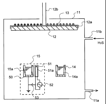
One exemplary arrangement of the system for forming the
light-emitting layer of the present invention is shown in Fig.
1. Here, SmAl2S4 : Eu is used as an example. As shown, the system
comprises a vacuum chamber 11 in which a substrate 12 on which
the light-emitting layer is to be formed, a K-cell 14 providing
an Sm evaporation source and an EB evaporation source 15 providing
an aluminum sulfide evaporation source are located. The vacuum
chamber 11 has an evacuation port 11a via which the vacuum chamber
11 is evacuated to a given degree of vacuum. The vacuum chamber
11 has also a feed gas inlet port llb via which hydrogen sulfide
gas (H2S) is introduced thereinto.
CA 02344011 2001-04-17
-12-
The substrate 12 is fixed to a substrate holder 12a having
a shaft 12b that is rotatably mounted by rotating shaft fixing
means (not shown) while the degree of vacuum is maintained in
the vacuum chamber 11. The shaft is rotatably driven by driving
means (not shown) at a given rpm, if required. Heating means
13 made up of a heater wire, etc. is fixed to the substrate holder
12a in close contact relation thereto to heat the substrate to
the desired temperature and hold the substrate at that
temperature.
The Sm metal material 14a to be evaporated is received in
the K-cell 14 that provides an Sm evaporation source. This
K-cell 14 is heated by heating means (not shown), so that the
metal material can be evaporated at the desired rate of
evaporation. The EB (electron beam) evaporation source 15 that
provides the aluminum sulfide evaporation means includes a
crucible 50 for receiving aluminum sulfide 15a with a light
emission center added thereto and an electron gun 51 with a
built-in filament 51a for the emission of electrons. The
electron gun 51 is connected with an alternating-current power
supply 52 and a bias power supply 53.
In this system, a vapor of the Sm material evaporated from
the K-cell 14, a vapor of aluminum sulfide evaporated from the
EB evaporation source 15 and the hydrogen sulfide gas introduced
into the vacuum chamber 11 are deposited and combined with one
another on the substrate 12 to form a light-emitting layer. If,
in this case, the substrate 12 is rotated at need, it is then
possible to make uniform the composition and thickness
distribution of the light-emitting layer to be deposited. It
is here noted that to say nothing of Sm and aluminum sulfide,
the materials necessary to form the desired thin film may be
charged in the K-cell 14 and the aforesaid evaporation source
15.
With the fluorescent thin film material and fabrication
process by evaporation according to the present invention, it
is thus possible to easily form a fluorescent thin film capable
of emitting light at high luminance.
CA 02344011 2003-12-22
-13-
Fig. 3 is a partly sectioned perspective view illustrative of
the structure of an inorganic EL device using the light-emitting layer
of the present invention. As shown in Fig. 3, a lower electrode 25 in
a given pattern is formed on a substrate 21. This lower electrode 25
is provided thereon with a thick film form of first insulating layer
(thick-film dielectric layer) 22. The first insulating layer 22 is
provided thereon with a light-emitting layer 23 and a second
insulating layer ( a thin-film form of dielectric layer) 24 in this
order. The second insulating layer 24 is provided thereon with a
given pattern of upper electrode 26 in such a way as to construct a
matrix circuit with the lower electrode 25.
Between adjacent members of substrate 21, electrodes 25 and 26,
thick-film insulating layer 22, and thin-film insulating layer 24,
there may be interleaved an intermediate layer such as a contact-
enhancing layer, a stress-relieving layer, and a reaction-preventing
layer. The thick film may be polished on its surface or improved in
terms of flatness as by using a flattening layer.
The substrate used should be formed of a material which has
a heat-resistant temperature enough to be capable of standing
up to a thick f,ilm formation temperature, an EL fluorescent layer
formation temperature and an annealing temperature for an EL
device or having a melting point of 6000 C or higher, preferably
700 C or higher, and more preferably 800'C or higher, and can
be provided thereon with a non-structural film such as a
light-emitting layer to form an EL device and maintain given
strength - To this end any desired material may be used provided
that it meets these requirements. For instance, ceramic
substrates such as alumina (A12O3), forsterite (2MgO=SiOz),
steatite ( MgO - SiOz ) , mullite ( 3AlO3 - .2SiQz ) , beryllia ( BeO ) ,
aluminum nitride (AlN), silicon nitride (SiN) and silicon
carbide (SiC+BeO) substrates and heat-resistant glass
substrates such as crystallized glass substrates are usable.
These substrates have all a heat-resistant temperature of about
CA 02344011 2001-04-17
-14-
1,000 C or higher. Of these, alumina substrates and
crystallized glass substrates are preferred. Where thermal
conductivity is needed, beryllia substrates, aluminum nitride
substrates and silicon carbide substrates are preferred.
Besides, quartz wafers, thermally oxidized silicon wafers
and metal substrates such as titanium, stainless, inconel and
iron substrates may be used. Where electrically conductive
substrates such as metal substrates are used, it is preferable
to make use of structure where a thick film having an electrode
therein is formed on the substrate.
For the dielectric thick-film material (the first
insulating layer), known dielectric thick-film materials may be
used. Preferably in this case, materials having relatively high
dielectric constants should be used.
For instance, materials based on lead titanate, lead
niobate and barium titanate may be used.
The dielectric thick film has a resistivity of 108 S2 - cm or
greater, and especially of the order 1010 to 1018 S2=cm. The
dielectric thick film should preferably be formed of a material
having a relatively high dielectric constant c of about 100 to
10,000, and a thickness of 5 to 50 pm, especially 10 to 30 pm.
Preferably but not exclusively, the insulating thick film
is formed by processes that enable a film of 10 to 50 pm in
thickness to be easily obtained, for instance, a sol-gel process
or a printing firing process.
When the printing firing process is used, a material having
a consistent particle size is mixed with a binder to prepare a
paste having a suitable viscosity. This paste is then formed
on the substrate by a screen printing process, followed by drying.
The obtained green sheet is fired at a suitable temperature to
obtain a thick film.
The thin-film insulating layer (second insulating layer),
for instance, may be formed of silicon oxide (SiOZ)1 silicon
nitride (SiN), tantalum oxide (Ta205), strontium titanate
(SrTiO3), yttrium oxide (Y203), barium titanate (BaTiO3), lead
titanate (PbTiO3), PZT, zirconia (Zr02), silicon oxynitride
(SiON) , alumina (A1Z03) , lead niobate and PMN-PT material which
CA 02344011 2001-04-17
-15-
may be used in a multilayer or mixed layer form. These materials
may be used to form an insulating layer by existing processes
such as evaporation, sputtering, CVD, sol-gel, and printing
firing processes. In this case, the insulating layer has a
thickness of preferably 50 to 1,000 nm, and especially of the
order of 100 to 500 nm.
The electrode (lower electrode) is located, at least, on
the substrate side or in the first dielectric material. The
electrode layer that is exposed along with the light-emitting
layer to high temperatures for thermal treatments during
thick-film formation is formed of an ordinarily used metal
electrode composed mainly of two or more metals selected from
palladium, rhodium, iridium, rhenium, ruthenium, platinum,
tantalum, nickel, chromium, titanium, etc.
Other electrode layer defining the upper electrode should
be transparent to light in a given light emission wavelength range,
because emitted light is usually extracted from the side opposite
to the substrate. If the substrate is transparent, then the
transparent electrode can also be used for the lower electrode
because the emitted light can be extracted from the substrate
side. In this case, it is particularly preferable to use a
transparent electrode such as a ZnO or ITO electrode. Usually,
ITO contains In2O3 and SnO in the form of stoichiometric
composition; however, the amount of 0 may deviate slightly from
this. The mixing ratio of Sn02 with respect to In2O3 should
preferably be 1 to 20% by mass, and especially 5 to 12% by mass.
In IZO, usually, the mixing ratio of ZnO with respect to In2O3
is of the order of 12 to 32% by mass.
The electrode may contain silicon. This silicon electrode
layer may be either a polycrystal silicon (p-Si) electrode or
an amorphous silicon (a-Si) electrode. If required, a
monocrystal silicon electrode may be used.
The electrode is mainly composed of silicon, and is doped
with impurities to ensure electric conductivity. Requirements
for the dopants used as impurities are to ensure given electric
conductivity; ordinary dopants used so far with silicon
conductors such as B, P, As, Sb and Al may be used. However,
CA 02344011 2001-04-17
-16-
B, P, As, Sb and Al are particularly preferred. The
concentration of the dopants is preferably of the order of 0.001
to 5 at%.
These materials are used to form an electrode layer by
existing processes such as evaporation, sputtering, CVD, sol-gel,
and printing firing processes. Especially when preparing a
structure wherein a thick filmwith a built-in electrode is formed
on the substrate, it is preferable to make use of the same process
as in the dielectric thick film.
The electrode layer should have a resistivity of preferably
1 S2-cm or less and especially 0.003 to 0.1 S2-cm for efficient
application of an electric field to the light-emitting layer.
The electrode layer should have a thickness of preferably 50 to
2, 000 nm and especially of the order of 100 to 1, 000 nm although
varying with the material used.
While the application of the light emitting layer of the
present invention to an inorganic EL device has been described,
it is understood that the fluorescent thin film of the invention
may also be applied to a full-color display panel using other
forms of devices capable of emitting red, blue and green light.
EXAMPLES
The present invention is now explained more specifically
with reference to examples.
Example 1
One example of the evaporation system which may be used for
the fabrication process of the present invention is shown in Fig.
1. Here two electron guns were used instead of the K-cell.
An EB source 15 having A12S3 powders charged therein with
5 mol% of Eu added thereto and an EB source 14 having metal La
charged therein were placed in a vacuum chamber 11. The A12S3
powders and metal La were simultaneously evaporated from the
respective sources, and heated to 400 C to form a film form of
LaAlZS4 : Eu layer on a rotating substrate. The rate of evaporation
from each evaporation source was controlled in such a way that
the rate of deposition of LaAlZS4 was 1 nm/sec., and the molar
ratio of La: A12S3 was 1: 1. In this example, HZS gas was introduced
CA 02344011 2001-04-17
-17-
at 20 SCCM into the evaporation system. The thus obtained thin
film was then annealed at 900 C in vacuum for 10 minutes.
By fluorescent X-ray composition analysis, the LaA12S4 : Eu
thin film was found to comprise, in atomic ratio, La : Al : S: Eu =
12.3:25.1:50.0:0.65.
Using this light-emitting layer, an EL device was
fabricated. By applying a 1 kHz electric field having a pulse
width of 50 s to the electrodes, a blue emission luminance of
300 cd/mZ could be obtained with high reproducibility.
Exam8le 2
Example 1 was repeated with the exception that Nd was used
instead of the rare earth metal La and Ga2S3 was used in place
of A1ZS3. Substantially similar results were obtained. In this
example, green light was emitted.
Example 3
Example 1 was repeated with the exception that Y was used
instead of the rare earth metal La and In2S3 was used in place
of A12S3. Substantially similar results were obtained. In this
example, red light was emitted.
Example 4
Example 1 was repeated with the exception that Eu was used
instead of the rare earth metal La and Ce was used in place of
Eu. Substantially similar results were obtained. In this
example, blue light was emitted.
With the fluorescent thin film of the present invention,
it is thus possible to achieve red, green and blue fluorescent
thin-film materials which can emit light at higher luminance yet
with satisfactory color purity, and achieve high luminance using
the same film-forming method or system.
By using a fluorescent matrix material and a light emission
center material that are chemically or physically similar in
properties to each other according to the present invention, it
is possible to simplify a full-color EL panel production process,
thereby providing a fluorescent thin film which is less
susceptible to luminance variations and can be produced in
improved yields and so at lower costs.
CA 02344011 2001-04-17
-18-
The fabrication process of the present invention enables
composition control to be effected with improved reproducibility,
and provides a solution to sulfur-deficiency and
contamination-with-impurities problems in conjunction with the
sulfide defining the matrix material of the fluorescent thin film,
so that a light emitting layer of improved luminance can be
obtained.
EL devices using such a thin film are improved in terms of
light emission capabilities and practical utility, because
especially when multi-color EL devices or full-color EL devices
are fabricated, light emission layers can be fabricated with
improved reproducibility.
ADVANTAGES OF THE INVENTION
According to the present invention, it is thus possible to
provide a fluorescent thin film which can dispense with any filter
and has satisfactory color purity, and is particularly well fit
for RGB full-color ELs and its fabrication process as well as
an EL panel.
It is also possible to simplify a full-color EL panel
production process, thereby providing a fluorescent thin film
which is less susceptible to luminance variations and can be
produced in improved yields and so at lower costs and its
fabrication process as well as an EL panel.