Note: Descriptions are shown in the official language in which they were submitted.
CA 02344226 2001-03-27
PATENT APPLICATION
MICRO-OPTIC LENS WITH
INTEGRAL ALIGNMENT MEMBER
CROSS REFERDNCED TO RELATED APPLIC ATE
This application is related to pending U. S. Application No. 091162,455,
entitled
"MICRO-OPTIC LENS WITH INTEGRAL ALIGNMENT MEMBER", filed on
September 28, 1998.
TF('H1VICNAL FIELD
The present invention relates generally to micro-optical lenses, particularly
cylindrical
microlenses, and more particularly to cylindrical microlenses particularly
adapted to passive
alignment or semi-passive alignment. Such cylindrical microlenses may be
passively or semi-
passively aligned with electro-optical devices, including laser diodes and
integrated optics, as
well as other optical, electrical and electro-optical devices.
BACKGROUND ART
Semiconductor laser diodes are efficient sources of laser radiation, however
the highly
divergent beam emitted from a semiconductor laser diode presents problems in
many
applications. The divergence of the semiconductor laser diode's beam is caused
by its exit
aperture which is very narrow along one axis {the "fast" axis, which is
defined to be
perpendicular to the laser junction), and much wider along the perpendicular
axis (the "slow'°
axis, which is defined to be parallel to the laser junction). These two axes
correspond to the Y
and X axes, as will be later explained. The cross section of the beam emitted
along the fast, or
Y, axis is highly divergent due to diffraction effects. In comparison, the
wider aperture, defined
along the X axis, emits a beam cross section that diverges only slightly.
Laser diodes, or more properly, semiconductor lasers, are generally
constructed
according to well-known principles of semiconductor manufacturing technology.
A discussion
of these principles can be found in Richard R. Shurtz II, Semiconductor~asers
and LEDs in
~ler~,-~~;~s Engi,~.Pr~° Handbook, 3rd ed. (hereinafter "Shurtz")
(Donald G. Fink and Donald
Christiansen, eds. 1989).
To correct the divergence of the output beam from a laser diode, one
particularly
successful methodology has been .to .direct that beam through a particularly
configured
CA 02344226 2001-03-27
.i
cylindrical microlens, and several patents and patent applications are
directed to furthering this
technology.
One such device of an early type is taught in U.S. Patent 4,731,772, as
referenced in
U.S. Patent 5,050,153
S Another method for the fabrication of cylindrical microlenses of the type
embodied in
the present invention is taught in U.S. Patent No. 5,155,631. According the
'631 reference, a
preferred method far fabrication of cylindrical microlenses starts by forming
the desired shape
as a glass preform. The preform is then heated to the minimum drawing
temperature of the
glass, and a fiber is drawn from it. The cross-sectional shape of the fiber
bears a direct relation
to the shape of the preform from which it was drawn, thus forming the polished
microlens.
During the drawing process, the lens surfaces so formed become optically
smooth due to fire
polishing.
In order to collimate the beam produced by a laser diode, the invention taught
in U.S.
Patent No. 5,081,639 teaches the mounting of a cylindrical lens optically
aligned with the laser
1 S diode to provide a beam of collimated light from the Y axis of the diode.
The laser diode
assembly taught therein includes a diffraction-limited cylindrical Lens having
a numerical
aperture greater than 0.5 which is used to collimate a beam from a Laser
diode. A collimated
beam is one which is neither converging nor diverging; i.e., the rays within
the beam are
travelling substantially parallel to one another.
U.S. Patent No. 5,181,224 illustrates the use of cylindrical lenses to (inter
alia) create
a slowly diverging beam light. This lens may be said to be "circularizing"
and, when installed
on any of a variety of laser diodes is available as the "CIRCULASER~" diode
available from
Blue Sky Research in San dose, CA.
In U.S. Patent Application Serial No. 081837,002, entitled "MULTIPLE ELEMENT
LASER DIODE ASSEMBLY INCORPORATING A CYLINDRICAL MICROLENS", there
is described another diode / microlens system in which the microlens does not
correct for
astigmatism of the diode beam, but which is instead corrected downstream with
a larger lens
or other means. In this system, no active alignment is required to position
the microlens
a
adjacent to the laser diode facet, so automation of the process is rendered
possible. However,
other means are then required to correct for the astigmatism of the beam.
These other means
take the form of additional optical elements inserted into the beam emerging
from the
microlens.
2
'~',~ CA 02344226 2001-03-27
In U.S. Patent Application Serial No. 08/837,004, a laser diode / cylindrical
microlens
assembly is taught in which a crossed pair of cylindrical microlenses is
attached to a substrate
on which is mounted a laser diode chip. The microlenses are mounted with their
flat surfaces
facing the emitting facet of the diode, which arrangement provides for passive
alignment and
S possible automated mounting, but requires no additional lenses for
astigmatism correction. The
crossed pair of lenses can collimate or focus the laser diode beam, for
example focusing the
beam into a single mode fiber.
U.S. Patent No. 5,050,/53 teaches a device related to the device taught in the
'772
teaching. In this teaching, the device is implemented as a semiconductor laser
optical head
assembly utilizing a tilted plate for astigmatism correction in place of the
cylindrical lens taught
in the '772 reference.
To overcome the loss of optical efficiencies inherent in each of these
designs, U.S.
Patent 'No. 5,181,224 utilizes a cylindrical microlens which with one optical
element
circularizes and corrects the astigmatism in the output beam of a
semiconductor laser diode.
1 S To obtain these advantages, the cylindrical lenses must be aligned to
tolerances less than 2
microns along at least one axis. This precision alignment has heretofore
required the active
alignment of the lens with the diode. The resultant apparatus, e.g., the
previously discussed
CIRCULASERTM, is a low-divergence, low numerical aperture, highly efficient
semiconductor
laser diode assembly, with properties unmatched by other laser diodes.
Indeed, the advantages accruing to the CIRCULASERTM are only obtainable by the
use
of microlenses. in optical systems of the type described in U.S. Patent
5,080,706, reducing the
size of the optical elements thereof is generally regarded as having positive
advantages in lens
fabrication and accuracy. Indeed, the performance provided by the use of
microlenses, i.e.
lenses not substantially larger than about 1000 microns in diameter, is not
attainable using
macroscopic lenses.
U.S. Patent Application Serial Number 08/725,151, entitled: '°ELECTRO-
OPTICAL
DEVICE WITH INTEGRAL LENS", teaches an improvement to prior active alignment
methodologies for mounting a long cylindrical microlens to a row of laser
diode chips which
has been cleaved from a wafer. According to this reference, the lens and the
diode row are first
positioned on a substrate. The long lens is then actively aligned to the diode
row by powering
at least one of the diodes and actively aligning the lens by inspection of the
resultant laser beam
formed in conjunction with the lens. Once aligned, the lens and diode are then
fixed to
..,
3
CA 02344226 2001-03-27
establish their relative position. Finally, the lens / diode row is cut into
individual diode chips.
In this manner, the alignment "cost" is spread over a number of devices. While
the
methodology taught in this reference presents a substantial economy over the
individual active
alignment hitherto required, there still exists the need to actively align the
diode row and the
microlens.
While the previously discussed laser diode assemblies are fully effective for
their
intended use, the method of their manufacture has heretofore resulted in
manufacturing
inefficiencies. In any optical system, the alignment of the various optical
elements is critical
to the functioning of the system. This is certainly the case where a
cylindrical microlens is
incorporated into an optical system with a laser diode to provide a low-cost
source of collimated
light. As is typical of many optical applications, there are six degrees of
freedom inherent in
the positioning of the lens with respect to the laser diode, as shown in
Figure 1. Having
reference to that figure, a cylindrical microlens, 100 is shown. The lens has
three axes, X, Y
and Z. The Z axis, 1, corresponds to the optical axis of the optical system.
The X, 3, axis is
transverse to the Z axis, 1, in the horizontal plane. The Y, 2, axis is also
perpendicular to the
Z axis but in the vertical direction. Positioning the lens along the X, Y, and
Z axes defines the
first three degrees of freedom. Furthermore, the lens may be rotated about
each of these axes
as shown at 10, 20, and 30, and each of these rotations also defanes a degree
of freedom with
regard to alignment of the lens in the optical system. For cylindrical lenses,
placement of the
lens along the X axis, 3, is often not critical. In summary, the accurate
alignment of a
cylindrical microlens with respect to a semiconductor laser diode often
requires precise
alignment of one with the other with respect to five degrees of freedom.
One reason that alignment is required between lenses and other optical
elements is that
minor variations in lens geometry and size require correction. Moreover, the
positionaI
tolerances required to achieve optimal optical performance are exceptionally
small: often less
than two microns. This is particularly true along the Z axis, where positional
accuracy is more
often critical than along the Y axis, for instance. The achievement of this
accuracy in posidonal
alignment has heretofore generally been accomplished by some means of active
alignment.
With respect to microlenses, the act of heat-pulling the preform to draw the
lens to its final size
can produce microlenses which are either slightly over-pulled or under-pulled.
Lenses having
these "pulling errors" may very well present optical properties which are
scaled versions of the
intended lens. This presents a problem in prior attempts at passive alignment
in that very small
,.
4
CA 02344226 2001-03-27
differences in physical dimension require different placement of the lens with
respect to one or
more degrees of freedom to effect proper alignment of the lens with respect to
the diode or other
device. While even a perfect lens has heretofore required some type of active
alignment,
pulling errors have absolutely mandated such a process.
$ A fairly typical active alignment methodology generally proceeds as follows:
First, a
section of cylindrical microlens is mounted on a small mounting bracket which
because of its
resemblance to a football goal post is referred to as a "goal post." It is
intended that rotation
about the X and Y axes is defined by the lens' position on the goal post.
After the lens is
mounted on the goal post, the goal post/lens assembly is then optically
positioned along the Y
and Z axes, and the lens affixed to the semiconductor laser diode. In order to
perform these
several alignments, a laser diode, usually the diode to which the lens will
ultimately be
assembled, is energized and the diode's laser beam directed through the lens
to a screen. The
operator manipulates the lens along and about the several axes until the
projected beam meets
the required specifications for the assembly. In this manner, movement along
the several axes,
1$ as well as rotation about those axes is manipulated by an operator who
assembles each lens and
laser diode. The entire operation is very dependent on the skill of the
operator, as the optical
cement utilized first to affix the lens to the goal post and finally to the
diode introduces a
variable into the problem. This variable is engendered by the fact that the
surface tension of
the cement between the several elements on which it is used causes motion
between those
elements. This motion of course tends to misalign the optical elements. Active
alignment
methodologies are generally utilized to produce the devices taught in U.S.
Patent Nos.
5,081,639 and $,181,224.
The term "passive alignment", as used herein, defines a process whereby the
lens is
aligned with respect to another device solely by mechanical means and
thereafter secured in
position with respect to the diode or other device. Examples of such
mechanical means include
mechanical jigs, fixtures, alignment blocks, and the like. Passive alignment
does not require the
projection of a beam of light through the lens, nor indeed manipulation of the
lens with respect
to beam alignment or performance. Passive alignment relies solely on the
mechanical
alignment of the lens with respect to the diode or other device to achieve the
required optical
alignment.
The term "semi-passive alignment", as used herein, defines an alignment
methodology
whereby the lens is aligned with respect to another device along at least one
degree of freedom
.~
5
CA 02344226 2001-03-27
solely by mechanical means, i.e., passively. Examples of such mechanical means
include
mechanical jigs, fixtures, alignment blocks, and the like. Passive alignment
does not require the
projection of a beam of light through the lens, nor indeed manipulation of the
lens with respect
to beam alignment or performance. Passive alignment relies solely on the
mechanical
alignment of the lens with respect to the diode or other device to achieve the
required optical
alignment. Alignment with respect to one or more of the other degrees of
freedom, where
required, is effected by an active alignment scheme. The passive and active
alignment steps in
a semi-passive alignment methodology may be performed in any order.
Preferably, an ideal semi-passive alignment scheme performs the passive
portion of the
alignment along the most critical degree of freedom. This is often the
alignment along the Z-
axis. After all alignment is completed, the lens is secured in position with
respect to the other
device.
Significant effort has been expended to overcome the effects of pulling errors
on the
manufacturing efficiency of devices incorporating microlenses and other
optical devices or
elements. In general these methodologies, and the apparatus which perform
them, can be
divided into two classes: those which seek to increase the efficiency of the
previously discussed
active alignment process, and those which seek to achieve a passive alignment
between the
microlens and other optical elements.
While the method taught in U.S. Patent Application Serial No. 08/725,151
spreads the
active alignment "cost" over a number of devices, there still exists the need
to actively align the
diode row and the microlens taught therein. What is clearly needed is a
methodology which
will result in further substantial savings in skilled manpower currently
required to accurately
assemble a cylindrical'rnicrolens using current non-passive alignment
methodologies. This
advantage could be effected if some workable passive or semi-passive alignment
methodology
were made possible.
What is further needed is a methodology which enables the previously discussed
passive
or semi-passive alignment of a lens, particularly a cylindrical microlens,
with respect to an
electron device, particularly a laser diode, to less than 2 microns with
respect to one or more
degrees of freedom, most particularly along the Z axis of the microlens.
What is still further needed is a methodology which effects passive alignment
while
being relatively insensitive to changes in final microlens size resulting from
pulling errors.
What is yet further needed is a methodology which scales its alignment with
changes
6
- CA 02344226 2001-03-27
~. . .1
in size from one microlens to another.
The several references made herein to reference works and to issued and
pending patents
is to show the state of the art at the time the present invention was made.
These references are
herewith incorporated by reference.
pISCLOSIZRF OF THE IN~IENTION
The present invention teaches the use of at least one, and preferably a
plurality of,
alignment members formed integrally with the cylindrical microlens during its
manufacture.
The alignment members, or standoffs, may take several forms, but in the
simplest form
comprise an extension, or finger, of the proper optical length to effect at
least partial passive
alignment of the cylindrical microlens with another device, for instance a
laser diode.
The alignment members incorporate at least one reference surface to effect
alignment.
In one preferred embodiment, at least one alignment member incorporates a
plurality of
reference surfaces whereby as many as five degrees of freedom are referenced
and defined.
The cylindrical microlenses incorporating integral standoffs in accordance
with the
principles of the present invention can be used to manufacture a single
lens/diode pair, or, in
the alternative, can be used to fabricate a structure having a plurality of
diodes or other
electrical devices affixed to a length of cylindrical microlens, the diodes
and Lens forming a
unity whole. This unitary whole may then be divisible into individual
lens/diode pairs, or may
include several diodes per lens.
The methodology enables the completely passive alignment of a lens,
particularly a
cylindrical microlens, with respect to an electron device, particularly a
laser diode, to tolerances
of less than 2 microns. with respect to one or more degrees of freedom.
The methodoldgy effects completely passive alignment while being relatively
insensitive to changes in final microlens size resulting from pulling errors,
thereby scaling its
alignment with changes in size from microlens to microlens. This feature is
attainable because
of a startling discovery regarding the formation of integral alignment
members: changes in scale
of the microlens occasioned by pulling errors induce changes in scale of the
alignment
members, which changes tend to be in the direction of desired correction!
In other words, where a cylindrical microlens is subject to a pulling error,
the
proportional reduction of the integral alignment member provides a degree of
alignment
correction which is not only in the correct direction, but is generally at
least approximately
correct with respect to the scale of required correction. By way of
illustration, where a
1 1
7
CA 02344226 2001-03-27
microlens is over-pulled, resulting in a slightly smaller lens than is
desired, the correct
alignment action, previously accomplished actively, would to move the
microlens slightly
closer to the Laser diode. Utilizing the principles of the present invention,
the proportional
reduction of an integral alignment member occasioned by the reduction in scale
of the entire
S microiens results in the reduction in length of the alignment member, which
reduction is at least
approximately in the correct scale of the requisite correction. Assuming that
the integral
alignment member is properly scaled during formation of the preform, the
resultant microlens,
when passively aligned, will remain in alignment without recourse to an active
alignment
regime.
BRIEF DESCRIPTION OF THE DRAWINGS
Fig. 1 is a depiction of the several axes defined by a cylindrical lens, and
of the degrees
of freedom inherent in these axes.
Fig. 2A is a front perspective view of a cylindrical microlens incorporating
the
principles of the present invention.
Fig. 2B is a rear perspective view of the cylindrical microlens of Fig. 2A.
Fig. 3 is cross-sectional representation of the cylindrical microlens of Fig.
2A in
operative combination with a laser diode, showing the laser beam entering and
exiting the
microlens.
Fig. 4A is a front perspective view of a cylindrical microlens having a
plurality of
powered surfaces, formed in accordance with the principles of the present
invention.
Fig. 4B is a front perspective view of another cylindrical microlens having a
different
plurality of powered shrfaces, again formed in accordance with the principles
of the present
invention.
Fig. 5 is a front perspective view of a cylindrical optical spacer having no
powered
surfaces.
Fig. 6 is a cross-sectional representation of the cylindrical optical spacer
of Fig. 5 in
operative combination with a laser diode and a cylindrical microlens, showing
the laser beam
entering the spacer and exiting the microlens.
Fig. 7 is a is 'cross-sectional representation of the cylindrical microlens of
Fig. 2A in
operative combination with a second cylindrical microlens, showing the laser
beam entering
the second microlens and exiting the first microlens.
8
CA 02344226 2001-03-27 --
Fig. 8 is a rear upward perspective view of another cylindrical microlens
formed in
accordance with the principles of the present invention, further incorporating
a plurality of
reference surfaces.
Fig. 9 is a front perspective view of the device of Fig. 8., mounted on a
substrate and
in operative combination with a second, crossed, microlens.
Fig. 10 is a rear perspective view of the device of Fig. 9.
Fig. 11 is a perspective view of one embodiment of the present invention
wherein the
preform is implemented with discrete alignment members prior to formation of
the microlens.
Fig. 12 is a perspective view of a microlens resulting from the preform of
Fig. 11.
BEST MODE FOR PRACTICING THE INVENTION
Referring to Figures 2A and 2B, a simple cylindrical microlens, 102,
incorporating the
principles of the present invention is shown. Lens 102 is generally formed in
accordance with
the principles of the incorporated references, but with this difference: the
preform from which
the microlens is drawn is formed with at least one, and in this exemplar, a
pair of integral
alignment members or standoffs, 200 and 200'. Standoffs 200 and 200' extend a
distance "d"
from a first optical surface, 206, of the preform. In this embodiment, a
second optical surface,
204, is formed in lens 102 opposite first optical surface 206, but the
principles of the present
invention contemplate lens or other optical element configurations where this
is not the case.
Distance "d" is calculated to generate the proper alignment distance in the Z
axis (not shown)
from the device to which the lens will later be aligned (not shown in this
view). Moreover, the
longitudinally extending surfaces, 202 and 202' defined by the piano-linear
nature of standoffs
200 and 200', are reference surfaces which, in this embodiment enables the
passive alignment
with respect to three degrees of freedom: along the Z axis; about the Z axis;
and about the Y
axis.
Lens 102 is typically formed by the methodology of accurately forming a
preform
embodying all the features of the resultant microlens, then heating the
preform to about its
minimum drawing temperature, and finally pulling the microlens from the
preform. Where lens
102 is slightly over-pulled, resulting in a microlens of slightly smaller
profile than design
specification, distance "d" of standoffs 202 and 202' is likewise
proportionally smaller than
design specification. This proportional reduction of distance "d" enables the
advantages of the
present invention. The reduction of distance "d" acts to move optical surface
206 slightly closer
to the device, for instance a laser diode, to which microlens 102 is aligned
and attached. This
9
CA 02344226 2001-03-27
is exactly the correct direct to effect the desired correction occasioned by
the slight reduction
in scale occasioned by the over-drawing of lens 102. Moreover, the amount, or
scale of
reduction of distance "d" is at least approximately correct for the amount of
correction required.
An implementation whereby lens 102 is passively aligned with a laser diode 300
is
S shown at Figure 3. Having reference to that figure, lens 102 is indexed on
or aligned with a
surface of laser diode 300. Emitted from the surface 302 of laser diode 300 is
the widely
divergent beam 310 typical of such devices. One optical surface of lens 102 is
positioned a
fixed non-zero distance "d" away from surface 302 of laser diode 300 by means
of standoffs
202 and 202", which rest upon surface 302. In fihis embodiment standoffs 202
and 202' are
urged into contact with surface 302, but are not otherwise attached thereto.
One output beam,
for instance the circularized laser beam of the previously discussed
"CIRCULASER~" diode,
is shown at 320.
One alternative to this embodiment contemplates the attachment of lens 102 to
the
surface 302 of laser diode 300, at standoffs 202 and 202'. This attachment may
be
accomplished by any attachment technique well-known to those of ordinary skill
in the art.
These techniques include, but are not necessarily limited to, soldering;
brazing; the use of
adhesives, monomeric, polymeric or otherwise; eutectic bonding; thermo-
compression bonding;
ultrasonic bonding; thermo-sonic bonding; and other attachment technologies
well known to
those of ordinary skill in the art.
The previously discussed embodiment has focused on an implementation where a
first
optical surface is flat and its opposite optical surface is curved. The
principles of the present
invention specifically contemplate its adoption on optical devices having zero
to a plurality of
curved optical surfaces-'and incorporating at least one integrally formed
alignment element.
Referring to Figures 4A and 4B a pair of cylindrical microlenses 400 and 440
are
disclosed each of which feature a plurality of curved optical surfaces.
Cylindrical microlens
400 has a convex first optical surface 404 in operative and optical
combination with a second
convex second optical surface 402. Cylindrical microlens 404 has a concave
first optical
surface 410 in operative and optical combination with a second convex second
optical surface
408. While not illustrated herein, it will be obvious those having ordinary
skill in the art that
substantially any combination of concave, convex, or flat surfaces may, with
equal facility, be
implemented in accordance with the teachings of the present invention. The
present invention
specifically contemplates all such implementations.
CA 02344226 2001-03-27
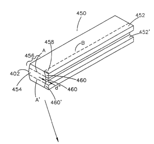
One embodiment of the present invention is particularly suitable to lens forms
which
do not lend themselves to internal grinding. One such form is shown in Figure
4 as 400. The
formation of optical surface 404 within a pair of alignment members 406 and
406' can be
difficult. The embodiment shown in Figures 11 and 12 obviate this difficulty.
Having
reference now to Figure 11, preform 450 is formed of at least two discrete
components. In this
exemplar preform 450 is composed of a first section defining optical surfaces
402 and 404, and
a pair of discrete alignment members 452 and 452'. Alignment members 452 and
452 may take
several forms. In one form, shown at 458, the alignment members are
substantially rhomboidal
elements having one face, 460 and 460', precisely matching the corresponding
portion of
optical surface 404. The edge of this embodiment is shown at "B".
A further alternative to this embodiment contemplates the formation of
alignment
elements which are substantially planar in aspect, and which form a portion
456 of at least one
optical surface. This alternative is shown at "A" and "A"'.
In either alternative, alignment elements 452 and 452' are precisely aligned
with respect
to preform body 454, and the assembly heated to at least the minimum drawing
temperature for
the preform material selected. Microlens 400, shown in Figure 12, is then
pulled from the
preform as taught in at least one of the incorporated references. The
heatlmeltlstretch sequence
serves to bond or weld the several elements of this embodiment into one
physical and optical
whole as shown at 400.
Another implementation of the present invention, wherein the optical element
includes
a plurality of flat surfaces, is shown at Figure 5. Having reference to that
figure, optical spacer
500 comprises an optical element having a first flat optical surface, 504 in
operative and parallel
optical combination with a second flat optical surface, 502. In this manner,
optical spacer can
serve to passively align a second optical device, not shown in this figure,
with a third device.
Similarly, optical surfaces 504 and 502 may, optionally, be formed in non-
parallel alignment,
thereby defining a micro-prism incorporating at Least one integrally formed
alignment element
or standoff.
One use for the device previously described and shown at Figure 5 is disclosed
at Figure
6. With reference to that figure, spacer 500 may be employed to effect a
desired alignment
between one optical device, in the case lens 600, and another device, here
laser diode 300.
Spacer 500 may be utilized to passively align cylindrical microlenses which do
not include
integral alignment elements, as shown in this figure, or to implement an
alignment distance
.~
11
CA 02344226 2001-03-27
greater than would be feasible utilizing exceptionally long integrally formed
alignment
elements. The divergent beam output from diode 300 is shown at 300 and the
resultant beam
formed by the operative combination of diode 300, spacer 500 and lens 600 is
shown at 620.
Again, the attachment of these several elements may be accomplished by any
attachment
technique well-known to those of ordinary skill in the art. These techniques
include, but are
again not necessarily limited to, soldering; brazing; the use of adhesives,
monomeric, polymeric
or otherwise; eutectic bonding; thermo-compression bonding; ultrasonic
bonding; thermo-sonic
bonding; and other attachment technologies well known to those of ordinary
skill in the art.
While the previous discussions have largely centered on the utilization of the
principles
of the present invention applied to the formation of cylindrical microlens /
diode devices, study
of these principles makes obvious the fact that they may, with facility, be
implemented on a
broad range of optical devices. One such implementation is shown at Figure 7,
where a
cylindrical microlens incorporating at least one integrally formed alignment
element, 700, is
passively aligned with, and subsequently attached to, a second lens, 702. In
this example, an
input beam, 730, is focused into lens 702, which lens further focuses it into
cylindrical
microlens 700 which forms output beam 720. The principles of the present
invention
specif cally contemplate the implementation of those principles on a broad
array of optical
devices including, but not necessarily limited to one or more: lenses; prisms;
etalons; diffraction
gratings; optical fibers; fresnel lenses; minors; holograms; holographic
diffraction gratings;
beam sputters; polarizing optical elements; wave plates; graded index optical
elements;
attenuators; filters; apertures; and apodizers in operative combination.
The previously discussed applications of the present invention enable the
passive or
mechanical alignment of a'cylindrical microlens with respect to another
device, for instance an
electronic device, along one axis. In the exemplars previously discussed, this
axis is often the
Z or optical axis, as this axis is often the most critical alignment in the
formation of an electro-
optical device. Study of the principles taught herein reveals that passive
alignment may be
accomplished with respect to the other degrees of freedom inherent in the
design of a cylindrical
lens. The principles taught herein specifically contemplate all such
embodiments.
Further, the use of a pair of alignment surfaces formed orthogonally to one
another, each
of which is orthogonal to the Z axis. This arrangement enables passive
alignment of a
cylindrical microlens with respect to another device with respect to five
degrees of freedom.
A simple implementation of this concept contemplates the use of one of the
surfaces of the
12
CA 02344226 2001-03-27 _,
microlens, for instance lower surface 210 shown at Fig. 2A as a second
alignment surface.
While the previously discussed implementations enabled passive alignment along
the Z axis,
by using surface 210 as an alignment surface in operative combination with
another surface of
the electronic device, passive alignment with respect to five degrees of
freedom is enabled.
Having reference now to Fig. 8, the use of a pair of alignment surfaces, 812
and 814,
formed on a cylindrical microlens, 800 is shown. Microlens 800 is formed with
a first and
second optical surfaces, 804 and 802; a first alignment surface, 814 and a
second alignment-
surface, 812. Microlens 800 also shows another feature which eliminates
registry errors
occasioned by formation errors at the junction of surfaces 812 and 814. This
feature is a relief
groove, 816, which ensures that only surfaces 812 and 814 are in contact with
electron device
300, thereby eliminating errors in forming the juncture of surfaces 812 and
814 from adversely
affecting the alignment process.
By implementing a microlens, as 800, with a pair of orthogonally disposed
alignment
surfaces 812 and 814, which surfaces are further orthogonally disposed with
respect to the Z
IS axis, passive alignment of the lens with respect to another device, here a
laser diode 300, is
enabled. This alignment is explained as follows: urging surface 314 into
intimate contact with
surface 814 aligns microlens 800 with diode 300 with respect to the Z axis.
Urging surface 312
into intimate contact with surface 812, in and of itself, aligns lens 800 with
diode 300 with
respect to the Y axis. If the two urging actions are performed in operative
combination with
one another, further advantages eventuate. The combination of the two
alignments not only
aligns the lens and diode along the Z and Y axes, but also aligns these two
elements around all
three axes. Hence the principles of the present invention applied as shown in
Fig. 8 results in
the alignment of lens 80b and diode 300 with respect to five degrees of
freedom.
Moreover, where a lens is slightly over- or under- pulled, acceptable
alignment is
effected without further action. This automatic correction for pulling errors
is explained as
follows: a small over-pull results in the proportional scalar reduction of
every dimension of the
lens. This reduction in scale occurs at all dimensions, including the length
of standoffs 810 and
810'. The required correction for a lens smaller than specified is to move the
lens closer to the
light source to the lens. The reduction in scale, and hence elevation, of
standoffs 810 results
in a proportional reduction of distance "d°'. When surface 814 of
microlens 800 is urged into
contact with surface 314 of laser diode 300, the reduction in distance "d"
occasioned by the
over-pull results in moving optical surface 804 of lens 800 closer to emitter
310 of diode 300:
I3
CA 02344226 2001-03-27
exactly the desired corrective direction along the Z axis. Moreover, the
surprising result
obtained during development of the present invention is that this correction
is not only in the
proper direction, but is also at least approximately correct with respect to
the required amount
of the correction. In other words, the scalar reduction in distance "d" is
acceptably close to the
perfect correction required to optically align the over-pulled lens for most
applications. Indeed,
initial experimentation by the inventor indicates that in many
implementations, the amount of
correction is precisely proportional to the degree of mis-pulling. A similar,
but opposite effect
occurs where the lens is under-pulled.
In similar fashion, an over-pull results in the scalar reduction of the
distance between
the centerline 820 of the microlens and alignment surface 812, hereafter
referred to as distance
"x". This action, like that previously discussed results in an automatic
correction in the correct
direction along the Y axis, and again, the amount of the correction is at
least approximately
correct.
By combining the alignment actions of mating surfaces 814/314 and 812/312,
further
advantages eventuate. The combination of the alignments results not only in
alignment along
the Z and X axes, but also, from geometry, about the X, Y, and Z axes.
Accordingly, passive
alignment of the lens to the diode or other device is achieved with respect to
five degrees of
freedom. One device implementing these principles is shown at Figures 9 and
10.
The present invention further contemplates methodologies whereby passive
alignment
is attainable along two axes and about all three axes of the lens.
Accordingly, it will be
appreciated that the principles hereinafter enumerated enable passive
alignment of a cylindrical
microlens with respect to another device with respect to five degrees of
freedom.
The previous 'exemplars of the present invention have discussed
implementations
wherein the integrally formed alignment members are substantially piano-linear
in aspect. The
use of a plurality of alignment surfaces formed at angles to one another
present further
advantages. An example of a device implementing such an arrangement is shown
at Figures
9 and 10.
Having reference to those figures, a first cylindrical microlens 900 is formed
with at
least one integral alignment member 908. Member, or standoff, 908 is further
provided with
a pair of alignment surfaces 910 and 912. In this embodiment reference
surfaces 910 and 912
are longitudinally disposed and orthogonal to one another, but alternative
angles may, with
equal facility, be implemented. This embodiment incorporates a relief groove,
914 which
t4
CA 02344226 2001-03-27
..
ensures that alignment surfaces 910 and 912 mate flushly with the device to
which the
microlens will ultimately be aligned. Cylindrical microlens 902 in this
example includes a first,
planar, optical surface 904 and a second optical surface 906 in operative and
optical cooperation
therewith. As previously discussed, substantially optical profile may, with
equal facility, be
implemented. A fiuther alignment member, 916 may also be provided. Study of
Figures 9 and
reveals that alignment members 908 and 916 are asymmetrical, and the
principles of the
present invention specifically contemplate the use of such in some embodiments
thereof.
Device 900 depicted herein is an embodiment of the present invention applied
to a
device of the type taught and claimed in U.S. Patent Application Serial No.
08/837,004, which
10 is herewith incorporated by reference. Device 900 further incorporates a
second cylindrical
microlens 1000, including a first optical surface 1002, as second optical
surface 1004, and a pair
of integrally formed alignment members 1006 and 1006'. Second cylindrical
microlens 1000
is, in this embodiment, mounted orthogonally to first cylindrical microlens
902.
Device 900 further includes: a laser diode 300; and substrate elements 920 and
930.
Laser diode includes an emitter, or "p" face 35, and at least two planar
surfaces 352 and 354.
The passive alignment enabled by the principles of the present invention is
explained
as follows: first microlens 902 is mated and mechanically aligned with laser
diode 300 by
placing surfaces 352 and 354 in juxtaposition with alignment surfaces 910 and
912 arrayed on
alignment member 908 of microlens 902. A clamp or jig (not shown) maintains
microlens 902
and diode 300 in perfect alignment while they are attached one to the other
utilizing any of the
previously discussed attachment methodologies. This alignment and subsequent
attachment
results in the passive alignment of cylindrical microlens 902 with diode 300
with respect to five
degrees of freedom: along the Z and Y axes; and about the Z, Y, and X axes.
Following attachment, the combined microlens / diode pair 9021300 may then be
further
mounted to a substrate, in this exemplar substrate elements 920 and 930. In
this exemplar
substrate elements 920 and 930 are generally planar members, the several
surfaces of which are
substantially orthogonal to one another. Again, a jig or clamp maintains the
alignment of the
microlens / diode pair 902/300 while it is attached to the several substrate
elements. Where the
substrate is a mufti-part structure, as shown in the present figures, the
attachment of microlens
/ diode pair 902/300 thereto may proceed either with the attachment of the
several elements of
the substrate, or as a discrete step in conjunction therewith
At this point, the resultant device could be used to form a device of the
9 t
IS
CA 02344226 2001-03-27
"CIRCULARIZERTM" type, previously discussed.
With the addition of second microlens 1000 to the assembly including microlens
I diode
pair 9021300 and substrate elements 920 and 930, a device of the type found in
U.S. Patent
Application Serial No. 08/837,004 may be passively aligned formed. The final
formation
proceeds as follows: the assembly including microlens / diode pair 902/300 and
substrate
elements 920 and 930 includes a surface, 932, of substrate element 930. By
carefully forming
surface 1008 of second cylindrical microlens 1000 to be orthogonal to its
other surfaces, the
simple placement of surface 1008 on surface 932 results in an orthogonal
relationship between
first microlens 902 and second microlens 1000. Additionally, integrally formed
alignment
members 1006 and 1006' of second microlens 1000 in operative combination with
surfaces 932
and 1008 provide the proper alignment with respect to all six degrees of
freedom of second
microlens 1000 and first microlens 902. The passive alignment of second
microlens 1000 with
first microlens 902 followed by attachment of second microlens 1000 to at
least one of surface
932 and first microlens 902 results in the crossed lens device taught in U.S.
Patent Application
Serial No. 08/837,004.
Finally, while the preceding discussion has centered on the notion of forming
one
microlens with one diode, study of U.S. Patent Application Serial No.
08/725,151 reveals that
the principles enumerated herein are further applicable to that technology,
and to devices
formed thereby. Indeed, the principles of the present invention specifically
contemplate the
elimination of the active alignment taught in that reference, thereby
rendering it an even greater
improvement over prior active alignment schemes. U.S. Patent Application
Serial No.
08/725,151 is herewith incorporated by reference.
The present invention has been particularly shown and described with respect
to certain
preferred embodiments of features thereof. However, it should be readily
apparent to those of
ordinary skill in the art that various changes in modifications in form and
detail made be made
without departing from the spirit and scope of the invention as set forth in
the appended claims.
In particular, changes in materials, dimensions, optical prescriptions, lens
geometries, optical
device descriptions, attachment methodologies, number of alignment elements
and alignment
surfaces as well as alignment surface angles needed to meet the requirements
of a particular
application are specifically contemplated by the principles of the present
invention. The
invention disclosed herein may be practiced without any element which is not
specifically
disclosed herein.
9
16