Note: Descriptions are shown in the official language in which they were submitted.
WO 00/17960 PC'T/US99/20699
-1-
ANTENNA ARRAY STRUCTURE STACKED OVER PRINTED
WIRING BOARD WITH BEAMFORM1NG COMPONENTS
BACKGROUND OF THE INVENTION
The users of computers, Personal Digital Assistants (PDAs), and other data
processing equipment increasingly rely upon various types of network
connections
in order to obtain access to data in various forms. For example, sophisticated
business users now desire high speed Internet access whether on the road or in
their
home location. Corporate information technology departments often need to
rapidly set up and tear down access for their users as locations change and
to temporary visitors need to be accommodated. In addition, organizations in
the
appliance repair, package delivery, and other service industries also require
data
access.
Although present wireless communication infrastructure such as provided
by the cellular telephone network is in widespread use for voice traffic, its
use has
not spread in particular for data applications. This is due in part perhaps to
the
relatively slow available speeds for sending data over cellular connections,
which
supports rates of only 9600 or 14400 baud. Another consideration is
convenience.
For example, in order to use the cellular system, one must not only carry
around a
cellular telephone, but also specialized modem equipment in addition to a
laptop
2o computer or other personal computing equipment.
Digital cellular equipment typically makes use of handsets that have the
traditional single dipole antenna. Unfortunately, such antenna units are not
optimized for maximizing data speeds. For example, in networks that make use
of
Code Division Multiple Access (CDMA) signaling, power levels must be carefully
controlled, especially for transmission from the subscriber back to the base
station
(reverse link). By optimizing the effective radiated power, data rates can be
maximized.
Unfortunately, known dipole antenna arrangements, or even known
combinations of dipole arrangements, do not provide adequate control over
CA 02344265 2001-03-16
SEP-11-2000 MON O1~IB PM H$S&R FAx N0. 7818821028 p, lp
,.2-
ct>('ectlve radixleet power. This is due in pant to a number oFcausoa. Dipole
ant~~nna.R alone do net provide dirootional antenna patterns that allow 1ha
power to
be more et~ctivEly dltcctcd to the base station. Moreover, irnplcnZCntinE such
devicoe within handset form Factors, or within other form factors such ac
integral to
thu evse ofthe computer equipment, makes it dilTicult to ensure that thn
anten~~a
elements am pcoporly oriented with rc~sp~t to the earth.
What is needed is a small and convenient unit that cttn be used to provide
wireless dale access such as over existing cellular telephone networks. 1'he
device
should have a convenient Co.cra factor such as will ilt in a shin pocket or
purse.
U.S. Patent S,G28,053 issued to Aralti ec al, discloses an intagralc~d multi-
laycr microwave circuit that contains au antenna portion formed from a
microstrip
circuit llne. The antenna may bo mounted on a vehicle to external portions of
ihc
vehicle such as roof, trunk, mirrors, windshields, dashboards and the like.
?hc
antcmt.~ disclosed therein ptbvldes a directional radiativrt pattern, however
the
radiation pattern may nol he ohungod or stored,
French Patent 2 714 195 discloses an antenna circuit assembly consislin~ of
a number of antenna el~rncnts; tlic atttelma is intended for operation at
extremely
hi~:h mictuwavc frcyucncics of 60 Gignlicriz (GHy.) ormoro.
F,uropean Patent 0 793 293 discloses an antenna uwt that enctose:s a power
supply conductor within cut antenn:~ body.
U.S. Patent 5, 6$0,14.4 issued to 5m~ad discloses the use of double G type
patch antenna elements ~or use in a communication device such as a cellular
telephone.
AMENDED SHEET
~P~am~
ONTUANGEN 11-OO-2000 1D:16 UAN-Tii1A6I10IO NAAR-EPO/EPA/OEB TN DG1 PAG'S 010
CA 02344265 2001-03-16
SEP-11-2000 MON 01.18 Ptt NBS&H hAx nu. raloa~lu~a r. 11
PCiYUS99/zOG99 _~_
SiJMMAttY OF T1:1~ 1NVENTTON
'fho present invention is a miniaiuriied dircation~l ltnteruta array that can
bo
used to provide dircctianal gain to optimize digital dais communications. The
antenn:c arrlty is packaged W a palm sized case which rslay be placed on a
tabld or
alher approximately hori~onlal surface convenient to the poriablc compelling
cduipmcnt. The arrangancnt of the array elements within flit case
automatical)y
hrovidas a proper orlcntalion of the antenn7 elements wish respect to the
earth.
Tn the profcrrad enibodimcnt, the array is a five clcmcni array having a
cclrtc,~r element and four outlying or corner clEments. Tha outlying elcntcnts
arc
spa~oed at eppmximately one-quaztcr of a wave length radial distance from the
center ctcment. 1'hc antenna clcrucnts are fastened to an appropriate support
structure disposed within the case which is formed of a convenient material
such as
plastic which is trattsparenl to radio wave propagation. Oilier clcctricltl
clcnicnis
- such as strip line power dividers, phase shifter components, and power
routing
components arc; placed on a multilayer printed circuit card disposed beneath
the
antenna array support siructuru.
1n the prefo~*ad embodinr<cni, the radiating elements thcmsalvcs ate a lyh~
of miniaturi-reti antctu~a clement known as a multilaycr chip antenna. Such
chip
antennas are extremely small in size and may be convcnicntly mounted within
the
support strucluras iu accordance with well known azanufacturing toohniyucs.
lllternatively, lhc Tadiatin~ elements may be helical antennas that arc also
mounted within the support structure with the proper vetlicaI orienlaNon.
The overall result is an antenna packame ihat does not exceed
aPproximatcly ~.5 centimeters (cm) in height and 7.5 cm in width and depth,
which
cml bc; used to greatly enhance the radio link signalfng characteristics for
Gala
sixnals.
t~RILzF DRSC1ZIPTfON 01~ T1~>? DRAWINGS
The forc;;oing and other obJccts, features and Advantages of the invoniian
will be apparent fmm the following more particular description of prclcrrcd
embodiments oFthe invention, as illustrated in the accompanying drawings in
AMENDED SHEE'~'
_ I PEA,~EP
ONTUANGEN it-09-2000 19:16 VAN-T81B621028 NAAR-EPD/EPA/OEB T11 OGi PAG'S 011
CA 02344265 2001-03-16
SEp-11-2000 tlOH 01:1 ? ptt Ii9S&R FAX N0. 7818821029 P. 12
1'C'f/U.~99I20G99 - 3A -
wllich like reference oharactess refer to the same parts throughout the
diffeceut
views. The drs~wtngs are not uecessadly io xalc. emphasis instead being plaood
upon illustrating the principles of the invention.
Fig. 1 is an external view of an antenna unit and a cOruputer interface cant
according to lltc invention.
Fig. 2 is a more detailed view of the inierlor of lha antenna unit.
trig. 3 is a more detailed view of a ohip muhi-layer antenna olemectt.
Fib. 4 is a luore detailed view of a helical antenna element lilat may ba used
in the array.
Figs. S, G snd 7 are antalu>la pattarns rautting from a sitttulation of an
untwma array structure according to ihc invcntioa.
hRTAlLI3U DE,SCit)fP'ftON OF THI: xNVEN'flON
Turning attention now to the drawings, Fig. 1 is an isometric vlcw of ati
untcuna uni l 10 according to the invention. Tha antenna unit t 0 is a
generally
roctaryular cans fora~ad of material such as plastie that is transparec>lt to
radio
wavc;s. The antenna unit 10 is connected via a bi-directional coatrol cable 11
over
a suitablQ computer intcrfi,ca such as a PCMCTA interface card 12.
The exterior of the antenna unlit 10 is typically labeled wiih an indicator
such ns an arrow 14 to u~struci ihc user on the proper orientation of iho
unit. _
t)uriag opcrcltiou, the unit 10 is, for example, placed on a table or desk or
oilier
convenient horiscontal surface and connected to the computing equipment such
as a
laptop portable coruputor, personal digital assistant (PhA), or other
eottaputing
device via the !'CMCIA card 12. The user cnsuros that the arrow is pointing in
the
upward direction.
The antenna unit 10 encloses not oily radiatit>~ arltonna elements but also
cirCUitly including radio frequency (RF), intermcdiats froqucilcy (1F), and
digital
circuitry on one or more layers 1G oCaprinted circuit board. The circuit
layers 1G
an; gCnerally indicated in Fib. 1, with the understanding that they may also
be
implemented on mere than ouc printed circuil~board.
Pig. 2 is a more detllilcd exploded view of the unit 10. The unit 10 includes
within the interior thereof an antenna array 20 and multiple circuit board
layers
AMENDED SHEE'~'
IPEA/EP
ONTYANGEN it-OA-2000 19:16 VAN-1818621Dx9 NAAR-EPO/EPA/(1E8 TN OG1 PAG'S 011
CA 02344265 2001-03-16
WO 00/17960 PCT/US99/20699
The exterior of the antenna unit 10 is typically labeled with an indicator
such as an arrow 14 to instruct the user on the proper orientation of the
unit.
During operation, the unit 10 is, for example, placed on a table or desk or
other
convenient horizontal surface and connected to the computing equipment such as
a
laptop portable computer, personal digital assistant (PDA), or other computing
device via the PCMCIA card 12. The user ensures that the arrow is pointing in
the
upward direction.
The antenna unit 10 encloses not only radiating antenna elements but also
circuitry including radio frequency (RF), intermediate frequency (1F), and
digital
1o circuitry on one or more layers 16 of a printed circuit board. The circuit
layers 16
are generally indicated in Fig. 1, with the understanding that they may also
be
implemented on more than one printed circuit board.
Fig. 2 is a more detailed exploded view of the unit 10. The unit 10 includes
within the interior thereof an antenna array 20 and multiple circuit board
layers
16-1, 16-2, 16-3, and 16-4 as previously mentioned. The antenna array 20 in
the
preferred embodiment consists of five antenna elements 22-1, 22-2, 22-3, 22-4,
and
22-5 arranged as shown. In particular, a center element 22-1 is arranged with
four
outlying elements 22-2, 22-3, 22-4, and 22-5 placed on the outer corners of a
generally rectangular frame used as a support structure 24.
The support structure 24 consists of a number of vertically oriented
surfaces including a back wall 25-1, a front wall 25-2, a right side wall 25-
3, a left
side wall 25-4, and a center wall 25-6. The center wall 25-6 supports the
center
element 22-1. The right hand wall 25-3 supports the rear right element 22-3
and
forward right element 22-4. The left wall 25-4 supports a rear left element 22-
2
and a front left element 22-5.
In this embodiment, the elements 22 are chip multilayer antennas such as
the model LDA36D1920 antenna available from Murata Manufacturing Company
Ltd. This type of element is described in further detail in connection with
Fig. 3.
The spacing between the elements 22 is critical to proper performance of
3o the array 20. In the preferred embodiment, the spacing of the array
elements 22
depends in particular upon the wavelength, ~,, of the intended center
frequency of
CA 02344265 2001-03-16
SEP-11-2000 MON 01:17 PM HBS&R FAX N0. 7818821028 P. 13
PC'.T/US99/20699
operation. in the proferrGd embodiatcnt of operation within the Personal
Communication System (1?CS) frequency bands of approximately 1850 to 1990
Ml~t2, the wavelength ~, i8 approximavtely 6.215 inches.
1u general, however, thc_clcmcnt spacing is auch that the center points of
the outlying etemeats 22.z, .... 22-5 are sat at a radial distnnee of
approxiinatoly
0.2G times ~, from the center element 22-I. It should be understood that this
spacing can ha varied somewhat in order to obl~ia desired effects. The array
ahouTd be a square afray such that the spacing should bo the same among all
adjacent outer elomcnts. hor cxaniple, the best spacing between front elements
ZZ-5 and 22-4 ie approximaloly the squaro root of 0.26 dma.4 ~, whioh is the
samo
as tito spacing between the elements along the side clcmc»ts Z2-2 and 2Z-5.
For
operation at approximately 1200 MHO, the entiro unit 10 is only about 7.5
_ ccntimctors (cm) by 7.5 cm by 2.5 high. -
1'ho support struclaro 24 can also be formed of any convenient material
transparent to the transmission of radio waves such as plastic, ceramie,~or
other
materials. What is important is that the support structure 24 orient the
antenna -
clelnents in a predictable way with respect to the earth. Thus, when the user
places
the antenna unit 10 with the correct orientation as indicated by the arrow 14,
ate
cloniQnls 22 wilt havo a known oriEtttaiion with respoct to the earth, and
more
prcdict<lblc operation t-esults.
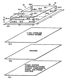
The arzay 20 also requires other components in order to properly operato.
For example, the array 20 is a dirdciionai array which can be steered in a
number of
different directions by aheuwging the phase of the electrical signals applied
to the
individual clcrnents 22. Thus, additionsl components such as power dividers,
phase shifters, and signal routing fracas are also placed and formed within
the
antenna unit 10. Preferably these components are placed within one of the
circuit
board layers 1G as previously described, For oxample, an upper layer 16-1 may
be
a ground plsno layer, and a second layer 1 G-2 may aocommodata-strip line
power
dividers to nrovidc five way splitting of elcclrical signal encryry applied to
the
antem,a array 20. A third laycx 16-3 may provide anothor ground piano and
fourth
AMENDED SHEET
IPEAIEP
OHTIIAfIGEII 11-OH-2000 19:16 UAN-T81862102A dAAR-EPO/EPA/OEB TN DGt PAG'S 013
CA 02344265 2001-03-16
WO 00/17960 PCT/US99/20699
-6-
layer 16-4 may provide a surface for mounting and interconnecting phase
shifter
components, additional power dividing components, and signal and power wiring.
Conductors 26-1, ..., 26-5 are extended from a feed point of each of the
elements 22-1, ..., 22-5 to provide a connection to the electrical components
such
as the strip line power divider components on layer 16-2. The circuit boards
16
and/or circuit layer may be solid ground planes or have interruptions at
various
places to accommodate wiring.
The arrangement in Fig. 2 thus provides a structure for miniaturized
antenna elements forming a steerable array which, in a relatively small
package,
1o provides a known orientation of antenna elements in order to optimize
operation
such as, for example, in wireless digital data networks.
Fig. 3 is a more detailed view of one of the miniature antenna elements 22.
This particular element, as obtained from Murata Manufacturing Company Ltd.,
is
a miniaturized type of antenna known as the LDA36D series. The element 22 is
of
the top capacitive loading type has a substrate 30 on which are formed a laser
trim
line 30 and internal top loading structure 34. A feed end point 36 provides a
point
at which a connection to a feed line can be made. The element 22 may be
fabricated on a convenient material such as a ceramic substrate. The antenna
element acts as a one-quarter wave length type radiating element.
2o In an alternative embodiment, the antenna elements 22 may be
implemented as miniaturized helical antennas such as available from Toko
America, Inc. Elements such as the model HEAW-TO1-002 have an overall height
H 3 of approximately 1.32 inches. In the case of the instance of the use of
helical
antennas 40, they may be mounted directly to the underlying circuit layers 16-
1,
and therefore do not need as elaborate a support structure 24 as in~the case
of the
chip antennas 28. However, the structure 24 must provide a proper orientation
of
such helical coil antennas with respect to the earth so they will always be
placed in
a known orientation by the user.
Samples of the types of antenna patterns which appear to be achievable
3o with the antenna unit 10 are shown in Figs. 5, 6 and 7. Fig. 5 is an
antenna pattern
developed from a simulation of the structure with the antenna phases set to
CA 02344265 2001-03-16
SEP-11-2000 MON 01:1? Ptl HBS&R FAX N0. ?818821028 P. 14
' ' ~ rcYrms~orio~~~
optimize a disootionnl orientation with respect to zero degrees. )t
illustrates that
the geometry can bo used W obtain an acceptable beamwidili of approximately 30
dogrc,-ns.
Fiss. G and 7 show the re~ull wharf the phase olomant weights are optimized
for 22 degrees and aS dcgrcc$ atccring respectively. The relative mapitudc
o~ihe
rcswlts ofthc sinitllation indicaicd an expected dircct3onal gain
of~proximatoly 4
Qccibcls with respect to isotropic (dBi).
While this invention has bean p~uticularly ahowu and described with
references to proferrari embodiments thereof, it will bo understood Q~t scope
of lttc
invention is tlc~fincd by tltc appended claims.
AMENDED S~iEE'~
iPEA/EP
ONTVANGEfI 11-08-2000 18:18 VAN-T61a1a=10i8 NAAR-EPO/EPA/OEB TN DG1 PAG'S 014
r
CA 02344265 2001-03-16