Note: Descriptions are shown in the official language in which they were submitted.
CA 02345037 2001-03-21
1
Method for Producing a M:icrotransponder
BACKGROUND OF THE INVENTION
Field of the Invention
The present invention re)_ates to a method for producing a mi-
crotransponder, especially a microtransponder of the type
l0 having a circuit chip which contains the transponder elec-
tronics, and having in addition a coil metallization which
acts as an antenna.
1'i Description of Prior Art
Due to the development of contact-bearing and contactless
chip cards, a completely new and rapidly growing market for
electronic microsystems has come into existence. Integrated
20 circuits are nowadays i.n;stalled not only in large devices or
manually held systems, but they are installed so to speak
"naked" in chip cards. A consistent further development leads
to the so-called "throw-away electronics", the first repre-
sentative of which was the telephone card. More recent fields
2°_~ of use for this so-called "throw-away electronics" are elec-
tronic labels which necessitate economy-priced chips or mi.-
cromodules in economy-priced, ecologically acceptable sup-
ports. The simplest case of an electronic label would be a
contactless module embedded between two pieces of paper, the
3o contact module comprising an integrated circuit and an an-
tenna coil.
CA 02345037 2001-03-21
2
Transponder modules for electronic labels are disclosed in
the Patent Abstracts of Japan, publication number 0929?535A,
relating to the Japanese application 08109052 and the Patent
Abstracts of Japan, publication number 09293130A relating t:o
~> the Japanese application 08109051. In the case of the elec
tronic labels describeca in the above-mentioned publications
an integrated circuit chip together with an antenna are cast
in a film-like resin. This film-like resin is then introduced
into a metal mould where an outer resin is cast around the
to film-like resin.
The Patent Abstracts of Japan, publication number 090198481A,
relating to Japanese application 08005845 disclose an elec-
tronic label in the case of which a circuit chip and a loop-
1~~ type antenna are applied to a substrate, the outer end of the
antenna being connected t:o a terminal on the integrated cir-
cuit via a bridging metallization which is conducted over the
windings of the antenna and which is separated from these
windings by means of an insulating resin layer.
The Patents Abstracts of Japan, publication No. 08216573A,
relating to Japanese application 0'1021785 describes a con-
tactless IC card compri:>ing a circuit chip and an antenna
section. The circuit chip is attached to a circuit section
provided on a polyester film, the antenna section being
formed on this polyester film as well. By means of an adhe-
sive layer, a second polyester film, which embeds the circuit
chip, is formed on the first polyester film. In addition, a
third polyester film is applied to the surface of the second
3o polyester film by means of a further adhesive layer.
In DE 19639902 A1 contact.l.ess chip cards and methods of pro-
ducing the same are described. The chip cards described in
CA 02345037 2001-03-21
3
this publication comprise an electrically insulating, one-
piece card body having one or a plurality of openings on one
side thereof. Furthermore, a conductor pattern is provided on
the surface of the card body, the conductors being directly
applied to surface areas of the card body side provided with
at least one opening, and the openings having arranged
therein one or a plurality of chips which are bonded to at
least one of the conductors.
to A survey of known methods of applying integrated circuit
chips to a substrate, e.g. by means of a flip-chip method, is
contained in H. Reichl, et al: Packaging-Trends: "High-Tech
im Kleinstformat", Elektronik 12/1998 (or SMT Nurnberg 98,
Conference Proceedings).
SUMMARY OF THE INVENTION
It is the object of the prESSent invention to provide an econ~-
omy-priced method, which permits the production of ultraflat
microtransponders that are suitable to be used e.g. for elec-
tronic labels.
This object is achieved by a method for producing a micro-
transponder in the case of which an antenna metallization
having a first and a second connecting end is first applied
to a support substrate. Furthermore, a connecting metalliza-
tion is applied to a flexible support foil, whereupon a cir-
cuit chip having a first and a second connecting area is ap--
3o plied to the connecting metallization in such a way that at.
least the first connecting area of the circuit chip is con-
nected to the connecting metallization in an electrically
conductive manner. The support substrate and the support foil
CA 02345037 2001-03-21
4
are then joined in such .a way that the connecting metalliza-
tion is connected to the first connecting end of the antenna
metallization in an electrically conductive manner and the
second connecting area c~f the circuit chip is connected to
~~ the second connecting end of the antenna metallization in an
electrically conductive manner. Edge areas of the flexible
support foil are then joined to neighbouring areas of the
support substrate so as to encapsulate at least the circuit
chip.
1 C
It follows that the present invention provides a method for
producing a microtransponder in the case of which two modules
are initially formed, wh:ic:h are joined in the last step. The
first module comprises a support substrate, which may consist
15 e.g. of plastic material. or of paper and on which the antenna
metallization, i.e. the coil, i.s formed. The second module
comprises a thin support. substrate, which consists preferably
of plastic material, and which has applied thereto one or
more connecting metallizations and the circuit chip. These
zo two modules are then joined in such a way that the contacts
required for the electric connections between the coil and
the circuit chip are rea:l.i.zed. The support foil is then used
for encapsulating the circuit chip and optional further areas
of the coil metallization and of the connecting metalliza-
25 tions, respectively, by _joining edge areas of the support
foil with neighbouring areas of the support substrate by
means of welding or by means of an adhesive so that espe-
cially the circuit chip c.an be protected against external in-
fluences.
According to the present. invention, t:he two modules can first
be processed separately from one another so that one module
can be processed without taking into consideration the re-
CA 02345037 2001-03-21
spective other module. The two modules can then be joined in
such a way that, when they are being joined, all the neces-
sary electric connections will be established. Through-
contacts through the suf>port substrate, which are only re-
'_~ quired in the case of some embodiments, have to be estab-
lished in a separate step before or after the joining of the
two modules. When the two modules have been joined, the thin
support foil, which, on the one hand, serves to handle the
circuit chip and the connecting metallization, is used in ac-
to cordance with the present invention for encapsulating at
least the circuit chip and preferably also the areas in which
the connections between t:he connecting metallization and the
antenna metallization are realized, by joining edge areas of
this thin support foil to the support substrate by means of
welding or by means of an adhesive. This encapsulation is
carried out preferably i.n a vacuum or_ making use of a protec-
tive gas so as to prevent. an inclusion of possibly detrimen-
tal substances.
2o Embodiments and further developments of the present invention
are defined in the dependent claims.
BRIEF DESCRIPTION OF THE DRAWINGS
In the following, preferred embodiments of the present inven-
tion will be explained in detail making reference to the
drawings enclosed, in which respective identical elements are
designated by identical reference numerals.
Fig. la) to le) show a schematic representation for illus-
trating a first embodiment of the method according
to the present invention;
CA 02345037 2001-03-21
6
Fig. 2a) to 2d) show a schematic representation for illus-
trating a second embodiment of the method according
to the present invention;
Fig. 3a) to 3e) show a schematic representation for illus-
trating a third embodiment of the method according
to the present. invention;
Fig. 4a) to 4e) show a schematic representation for illus-
trating a fourth embodiment of the method according
to the present invention;
Fig. 5a) to 5e) show a schematic representation for illus-
trating a fifth embodiment of the method according
to the present :invention;
Fig. 6a) to 6c) show a schematic representation for illus-
trating a sixt=h embodiment of the method according
to the present :invention;
Fig. 7a) to 7c) show a schematic representation for illus-
trating a seventh embodiment of the method accord-
ing to the present invention.
DESCRIPTION OF PREFERRED EMBODIMENTS OF THE INVENTION
Making reference to Fig. 1, the first embodiment of the
3o method according to the present invention will now be ex-
plained in detail. As has been stated above, two separate
modules are first produced in the case of the method for pro-
ducing a microtransponder <3ccording to the present invention.
CA 02345037 2001-03-21
7
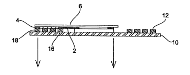
The first module produced is shown in Fig. la) . In the case
of this embodiment, a first connecting metallization 2 and a
second connecting metallization 9 are first applied to a thin
support foil 6, which consists preferably of plastic mate-
s rial, so as to produce this first module, which can also be
referred to as circuit chip module. Subsequently, a circuit
chip 8 is applied to the connecting metallizations 2 and 9.
The circuit chip 8 comprises the integrated circuit required
for the microtransponder and is provided with two connecting
to areas on or in one main surface thereof; for operating the
microtransponder, these connecting areas must be connected to
respective connecting ends of a coil antenna metallization.
The circuit chip 8 is app:L:ied to the connecting metallizatiori
2 in such a way that the first connecting area thereof is
15 connected to the first connecting metallization 2 in an elec-
trically conductive manner, whereas the second connecting
area thereof is connected to the connecting metallization 4
in an electrically conductive manner. This results in the
structural design of the i:irst module shown in Fig. la).
This first module is produced from extremely thin materials.
This is important in view of the fact that, when the micro-
transponder has been finished, the circuit chip 8 with thc~
support foil 6 should not. perceptibly project beyond a sup-
port substrate on which the coil met:allization is arranged.
The circuit chip and the foil preferably have a thickness of
less than 50 Vim.
The connecting metallizations 2 and 4, which may consist e.g.
of A1, Cu and the like, can be applied to the foil by arbi-
trary methods, e.g. by cladding and subsequent structuring,
by evaporation or sputtering and subsequent structuring, or
alternatively by evaporation or sputtering making use of a
CA 02345037 2001-03-21
8
shadow mask so as to apply lines which are already struc-
tured. The connecting metallizations may have a thickness of
less than 1 dun, since th.e conductor tracks of the connecting
metallizations can be implemented such that they are short
and broad. When the connecting metallizations 2 and 9 have
been finished, the circuit chip 8 is placed on the contact
areas of the connecting metallizations and is connected
thereto in an electrically conductive manner; this can be
done e.g. by means of thermocompression, anisotropic conduc-
1~~ tive adhesives or ultrasonic compression.
In Fig. lb) the second module is shown, which comprises a
support substrate 10 and an antenna metallization 12 applied
to a main surface of the suppart substrate 10. The support
1~5 substrate may consist e.<1. of plastic material or paper. The
antenna metallization 12,, which has the form of a coil, can
again be formed on the support substrate 10 by arbitrary
known methods. The coil metallization can e.g. be formed by
etching a cladding. Alternatively, a wire can be placed onto
2o the support substrate 10 such that a coil is formed. Accord-
ing to another alternative, a metal, e.g. Cu, A1 and the
like, can be applied to the support substrate 10 by evapora-
tion and structured subsequently. In order to obtain an ade-
quate thickness of the coil met.allization 12 the evaporated
2'. metallization can subsequently be thickened by means of an
electroplating technique. As can additionally be seen in Fig.
lb), a local thin insulating layer 14 is produced, e.g. by
means of a printing process, in an area of the coil metalli-
zation 12. This local insulating layer is produced in an area
30 onto which the second c:onnecti.ng metallization 9 will be
placed later on so as to prevent a short circuit between the
second connecting metal:lization 4 and the coil metallization
12.
CA 02345037 2001-03-21
9
At this point reference should be made to the fact that,
alternatively to the application of the insulating layer 14
to the coil metallization 12, this local insulating layer may
also be formed on corre:~ponding areas of the first module,
e.g. by means of a suitable printing process or by surface
oxidation of the metalliz<ition. Since the lines of the first
module are very thin in ~~~omparison with the antenna metalli.-
zation, which may have a thickness of e.g. 4 to 30 )tm, it may
to be more advantageous to form the insulating layer on the
first module, which is shown in Fig. la). The insulating
layer 19 can consist of an acrylic lacquer having a thickness
of 0.2 to 2 )tm, this acrylic lacquer being then locally re-
moved at the future contact points; this is done by means of
a thermal process. If the local insulating layer is formed on
the first module, this can be done prior to or subsequent to
the application of the c.i.rcuit chip 8 to the, connecting met-
allizations 2 and 4.
2o The first module and the second module are now joined in a
subsequent step, as shown in Fig. lc). In so doing, the first
connecting metallization 2 is connected to a first connecting
end 16 of the antenna metallization 12 in an electrically
conductive manner, whereas the second connecting metalliza-
tion 9 is connected to a second connecting end 18 of the an-
tenna metallization in an electrically conductive manner. In
the embodiment shown in Fig. 1, an isoplanar contact is ob-
tained in this way. As can be seen in Fig. ld) , the support
foil 6 is then connected along its edges to the support sub-
3o strate 10 in such a way that, in the embodiment shown, the
circuit chip 8 as well as the connecting areas between the
antenna metallization anc~ the connecting metallization are
encapsulated. This can be achieved by bending the edges of
CA 02345037 2001-03-21
the thin support foil 6 towards the support substrate 10 and
by subsequently joining the foil areas 20 abutting on the
support substrate 10 to the support substrate 10 by means of
welding or by means of an adhesive, as can be seen in Fig.
5 ld). It follows that, ac,~ording to the present invention, a n
encapsulation of the circuit chip and, in the case of the em-
bodiment shown, of the connection points can be accomplished
in a simple manner so as t.o provide protection against exter-
nal influences. This connection process between the support
1( foil 6 and the support substrate 10 is preferably carried out
in a vacuum.
A top view of the microtransponder produced by means of the
above method is shown in Fig. le). In this top view, espe-
1~~ cially the shape of the connecting metallizations 2 and 4 and
the arrangement of the insulating layer 19 can be seen.
Fig. 2 shows a schematic representation of a second embodi-
ment of the production method according to the present inven-
2o tion. The method shown in Fig. 2 corresponds essentially t:o
the method described with reference to Fig. 1, the support
substrate 10 having, however, provided therein an open-
ing/recess 30 into which the circuit chip 8 is introduced
when the first and second modules are being joined. The open-
25 ing 30 can be formed in l~he support substrate 10 by means of
arbitrary known methods. Since the support foil 6 and the
thin connecting metallization 2 provided thereon are flexi-
ble, the shape of the support foil 6 shown at 32 in Fig. 2c)
is obtained. One advantage of this embodiment of the method
3o according to the present invention is that the opening 30
permits an improved protection of the circuit chip 8 and
that, in addition, the circuit chip can be fixed more effec-
tively. The edge areas of the support foil 6 are again joined
CA 02345037 2001-03-21
11
to neighbouring areas of l.he support substrate 10 by means of
an adhesive or by means of welding so as to achieve an encap-
sulation of the circuit chip.
'i In Fig. 3 a third embodiment of the method according to the
present invention is schematically shown. In Fig. 3a) the
second module is shown,. which corresponds to the above-
described second module. In Fig. 3b) the first module is
shown, which also corresponds to the above-described first
1( module. Other than in the: case of the above-described embodi-
ments, the first and the second module are now, however,
joined in such a way that. the circuit chip 8 will be posi-
tioned on the surface of the support substrate 10 which is
located opposite the surface of the support substrate 10 hav-
1~~ ing the antenna metallization 12 formed thereon, cf. Fig.
3c). It follows that in 'the third embodiment shown, an elec-
trically conductive connection between the first and second
connecting ends of the antenna metallization 12 and the fir~;t
and second connecting metallizations 2 and 4 is not yet es-
20 tablished simultaneously with the joining of the first and
second modules. In order to realize this electrically conduc-
tive connection, through-contacts 90 and 92, respectively,
are established, cf. Fig. 3d). By means of the through-
contact 42 an electrically conductive connection is estab-
2~~ lished between the first connecting metallization 2 and the
first connecting end 16 of the antenna metallization 12,
whereas by means of the through-contact 90 an electrically
conductive connection is a>stablished between the second con-
necting metallization 4 and the second connecting end 18 of
3o the antenna metallization 12.
In order to establish the through-contacts, thermocompression
methods can be used by way of example. Alternatively, the
CA 02345037 2001-03-21
12
through-contacts can be produced by means of an ultrasonic
compression, by means of welding or by means of soldering. Fn
this respect, it should be pointed out that the through-
contacts may already be produced when the tt~o modules have
~~ not yet been joined, i.e. in the stage of the second module
which is shown in Fig. 3a), so that, when the two modules are
being joined, the respective electrically conductive connec-
tions between the through--contacts and the connecting metal-
lizations will be produce=d. As can be seen in Fig. 3e), the
to edge areas 20 of the support foil are again joined to
neighbouring areas of the support substrate 10 by means of
welding or by means of an adhesive, so as to encapsulate th.e
circuit chip and, in the embodiment shown, additional areas.
15 The fourth embodiment of t=he method according to the present
invention shown in Fig. 4 differs from the embodiment which
has been described with respect to Fig. 3 insofar as the sur-
face of the support substrate 10 located opposite the antenna
metallization 12 has formed therein an opening 50 into which
2o the circuit chip 8 is ir~t~roduced when the first and second
modules are being joined. As can be seen in Fig. 4c, this
permits an isoplanarity of the connecting metallizations 2
and 4. As in the case of the embodiment according to Fig. 3,
through-contacts 90, 92 .are again produced for establishing
25 an electrically conductive connection between the connecting
metallizations 2 and 9 and the first and second connecting
ends 16 and 18 of the antenna metallization 12. Furthermore,
also according to the fourth embodiment, the edge areas 20 of
the support foil 6 are joined t:o neighbouring areas of the
3o support substrate 10 by means of welding or by means of an
adhesive so as to effect an encapsulation.
CA 02345037 2001-03-21
13
In the case of the method shown in Fig. 5, a circuit chip Ei0
is used, which is provided with a first connecting area on a
first main surface thereof and with a second connecting area
on a second main surface thereof. The first module shown in
~~ Fig. 5a) is now formed by applying a single connecting metal-
lization 62 to a support foil 6. The circuit chip 60 is ap-
plied to the connecting rnetallization 62, an electrically
conductive connection being established between the connect-
ing area of the circuit chip 60 and the connecting metalliza-
tion 62 e.g. by means of conductive adhesives or by means of
soldering.
Fig. 5b) shows the second module; for producing this second
module, an antenna metall.ization 64 is first applied to a
support substrate 10. As can be seen in Fig. 5b), the antenna
metallization 64 has a preferably enlarged second connecting
end 66, the circuit chip 60, whose lower surface may be pro-
vided with a metallizat.i.on 68 thickening the connecting area,
being applied to this second connecting end 66 when the first
2o and second modules are be,i.ng joined. As has already been ex-
plained with reference to Fig. l, a local insulating layer 70
is formed on respective areas of the antenna metallization 64
also in the case of the embodiment shown in Fig. 5 so as to
prevent later on a short circuit between the connecting met-
allization 62 and the antenna metallization 69.
The first module is now ~~onnected to the second module, cf.
Fig. 5c), a contact between the metallization 68, i.e. the
second connecting area on the lower surface of the circuit
3o chip 60, and the second connecting end of the antenna metal-
lization 66 being established simultaneously, and an electri-
cally conductive connection between the connecting metalliza-
tion 62 and the first connecting end 72 of the antenna metal-
CA 02345037 2001-03-21
14
lization 69 being established simultaneously. As can be seen
in the detail representations shown in Fig. Sd), the edge ar-
eas 20 of the support foil 6 are connected, i.e. joined by
means of welding or by means of an adhesive, to corresponding
'S neighbouring areas of the support substrate 10 also in the
case of this embodiment. Fig. 5e) shows a top view of the re-
sultant microtransponder.
In the sixth embodiment of the method according to the pre-
l0 sent invention, which is schematically shown in Fig. 6, a
first module is again prepared, which essentially corre-
sponds to the first module shown in Fig. 5. This first module
is shown in Fig. 6b). The second module differs from the mod-
ule described with reference to Fig. S insofar as an opening
1~~ 80 is formed in the main surface of the support substrate 1.0
facing away from the antenna metallization 64, Fig. 6a). As
can be seen in Fig. 6c), the circuit chip 60 is introduced i.n
this opening 80 when the two modules according to this em-
bodiment are being joined" For establishing an electric con-
20 tact between the connecting area, or the reinforcement 6f,
arranged on the upper surface of the circuit chip and the
second connecting end 66 of the antenna metallization 64, it
is necessary to eliminate, preferably by means of a thermally
supported method, the web 82 of the support substrate ar-
25 ranged above the opening 80, so as to establish an electri-
cally conductive connection between the connecting area ar-
ranged on the upper sur-face of the circuit chip 60 and the
second connecting end 6Ei of the antenna metallization 69.
Furthermore, a through-contact 84 is produced so as to estab-
30 lish an electrically conductive connection between the con-
necting metallization 62 and the first connecting end 72 of
the antenna metallization 69. Also in the case of this em-
bodiment, the edges of the support foil 6 are joined to the
CA 02345037 2001-03-21
support substrate 10 by means of welding or by means of an
adhesive so as to obtain an encapsulation.
Also in the embodiment which is schematically shown in Fig.
~~ 7, a circuit chip 60 with double-sided contacting is used.
Other than in the case of the method described with reference
to Fig. 6, the support substrate 10 has now provided therein
an opening 90 which extends through the whole support sub-
strate 10 up to the second connecting end 66 of the coil met-
ro allization 69. The rest of the method for producing the mi-
crotransponder according to the embodiment shown in Fig. 7
corresponds essentially t:o the method which has been de-
scribed with reference to Fig. 6, but the heat treatment for
eliminating a web above the opening 90 can now be dispensed
1~~ with, since such a web does not exist. The other steps r~rre-
spond to the steps which have been described with reference
to Fig. 6.
It should be pointed out that the second connecting end 66 of
the antenna metallization 69 may cover the circuit chip 60
completely or partially. Furthermore, the metallization 68 Gn
the circuit chip 60 may cover the circuit chip completely or
partially; a person skilled in the art will also be aware of
the fact that, with the exception of the connecting area c>f
2~~ the circuit chip 60, a passivat:ion layer is arranged between
the metallization 68 and the circuit chip 60.
It follows that the present invention provides a simple tech-
nique for producing a microtransponder in the case of which
the production of the antenna module and the production of
the circuit chip module are completely separated. The circuit
chip module can be implemented such that it is much thinner
than the antenna module. Various production techniques can be
CA 02345037 2001-03-21
16
used for producing the antenna module and for producing the
circuit chip module. Due i.o the fact that the circuit chip .is
encapsulated or that large areas thereof are covered by a
metallization, good light protection can be achieved. The
methods according to the present invention are preferably
executed such that the individua:L modules are formed on an
endless material and are then sequentially supplied to a
processing station in which the modules are joined. The re-
spective metallic layers may consist of a ferromagnetic mate-
to rial so as to permit, if necessary, magnetic handling of the
individual modules or of the finished microtransponder. For
handling the thin circuit chip modu:Le, the circuit chip mod-
ule may be supported by an additional support so as to stabi-
lize it, whereby distortions or even rolling up due to inter-
lp nal mechanical stress can be avoided. The encapsulation of
the circuit chip and of additional optional areas is prefera-
bly carried out in a vacuum or while a protective gas, e.g. a
forming gas, is being supplied.