Note: Descriptions are shown in the official language in which they were submitted.
CA 02345570 2001-04-27
PROGRAMMABLE CIRCUTT WITH PREVIEW FUNCTION
BACKGROUND OF THE INVENTION
1. Field of Invention
This invention is directed to a circuit that can be both non-permanently
programmed and permanently programmed.
2. Description of Related Art
Fuses and fusible links are circuit elements that open by burning out or
breaking when a relatively high current is applied. By selectively breaking or
leaving
intact specific fusible links, a circuit can be customized or programmed using
these
fusible elements. An antifuse is the opposite of a regular fuse. That is, an
antifuse is
normally an open circuit until a programming current is forced through it.
Fuses and
antifuses may be used to address many problems, including calibration
requirements
of analog circuits such as digital/analog converters, or current or voltage
sources, logic
synthesis circuits such as digital delays lines, or chip specific performance
data to be
used by the end system in which the chip will be used. These fusible and
antifusible
circuits are generally "programmed" after chip fabrication has been completed
and
during the wafer testing phase of chip production. The programming may be used
to
add additional resistors into a circuit to compensate for variations
introduced during
the manufacturing process or to compensate for oscillator frequency variations
induced by manufacturing stress.
In many of these cases, it is desirable to simulate a programmed state before
actually programming the device. For example, analog circuit calibration may
require
additional steps of simulation and refinement based on the previewed or
simulated
results obtained. These results are incorporated into further simulations to
correctly
calibrate the circuit during the testing phase. After testing, the circuit may
then be
permanently programmed.
Conventional programmed circuits employing, for example, fuses and anti-
fuses, generally do not permit preview or simulation of the programmed
circuit.
Conventional programmed circuits require specialized packaging to ensure no
overlay
of the fusible or antifusible link occurs. That is, a conventional circuit can
only be
CA 02345570 2001-04-27
2
permanently programmed and not previewed. Once the conventional circuit is
programmed, no further changes or refinements to the circuit are possible.
U.S. Patent 6,037,871 to Watrobski et al. describes such a fusible link
circuit
including a preview feature that uses fusible links in combination with
transistors to
permanently set the value of an output. However, this fusible link circuit
also requires
special manufacturing and packaging techniques, as discussed above. For
previewable devices such as those described in Watrobski, the device imposes
specialized packaging, manufacturing, handling and cost limitations.
Conventional
fuse programming methods require that the selected device packaging technique
be
suitable for the programming structures. For example, the device packaging
techniques need to facilitate air access to the fuse for burning and to avoid
overlays
that may act as heat sinks. A heat sink would increase the fuse blow
temperature,
which could possibly exceed the circuit temperature tolerance. Thus,
manufacturers
of products requiring these features must select packaging and fabrication
techniques
that are tailored to these fusible circuits and which are typically more
expensive than
non-programmable circuit fabrication and packaging techniques.
Erasable programmable read only memory (EPROM) and electrically erasable
programmable read only memory, (EEPROM), devices may be programmed and re-
programmed. However, EPROM devices rely on specialized fabrication techniques
and typically include a quartz window through which ultraviolet light of a
specific
wavelength may be introduced for several minutes to erase the chip in
preparation for
re-programming. In use, the quartz window is covered to prevent accidental
erasure
of the device. The EPROM devices require physical removal of the chip and or
physical manipulation of the cover over the quartz window as well as
considerable
time to effect erasure in preparation for re-programming. Thus, EPROM devices
require both specialized fabrication techniques and specialized handling
during
programming.
EEPROM circuits typically use floating gates surrounded by a much thinner
insulating layer which can be erased by applying a voltage of the opposite
polarity to
the charging voltage to the non-floating gate. EPROM circuits overcome some of
the
EPROM device limitations with respect to the use of ultraviolet light to
effect erasure.
However, EEPROM devices also require special fabrication techniques in their
CA 02345570 2001-04-27
3
manufacture. Furthermore, EEPROM devices require that special "opposite
polarity"
voltage levels be adopted for reading and writing to the EEPROM device.
SUMMARY OF THE INVENTION
Conventional programmable circuits are either write-once circuits that can be
programmed but not re-programmed or read and write devices that can be
programmed and re-programmed. The write-once circuits do not provide for
simulating or previewing the state of a circuit before programming the circuit
permanently. The read and write devices can be re-programmed after simulating
or
previewing the circuit but require special handling and manufacturing
techniques.
Thus, a programmable circuit is needed that can be fabricated using
conventional reliable and inexpensive fabrication techniques and that provides
a
preview function which uses normal circuit voltage levels for permanent
programming and higher voltage levels for permanent programming.
This invention provides systems and methods for programming a circuit using
a pull-down transistor as an antifuse in the circuit.
This invention separately provides a circuit having a preview function useable
to simulate circuit characteristics using normal voltage.
This invention further provides a circuit that uses a higher voltage to
permanently program the circuit.
The circuit can be fabricated using conventional, inexpensive and reliable
fabrication techniques. The circuit includes a spike enable input structure
which is
used to determine when the chip is to be programmed. The circuit also includes
a test
and spike input structure which has at least two functions controlled by the
setting of
the spike enable input structure.
When the spike enable input structure is in the default or open state, a
programmable transistor is in an open state. As a result the voltage at the
output
structure is at a first predetermined value. External tester electronics can
be attached
to the test and spike input structure to drive the output structure to the
first
predetermined voltage by leaving the test and spike input undriven or by
driving the
test and spike input structure to the first predetermined voltage. Conversely,
the
external electronics can drive the output structure to a second predetermined
value by
driving the test and spike input structure to the second predetermined value.
Thus, the
CA 02345570 2001-04-27
4
output of the circuit can be simulated or previewed before permanent
programming of
the circuit occurs.
A programmed state of the simulated programmable previewable circuit can
be created by asserting an enable signal on the spike enable input. A test and
spike
input is then pulsed with a programming voltage that is higher than either the
first or
second predetermined voltages. The programming voltage is of sufficient
amplitude,
pulse width and frequency to cause the programmable transistor to enter the
failure
mode, known as snap back. During the snap back mode, the programmable
transistor
carries a large current density. The large current density in turn causes
silicon to
dissolve into the metallic layer connected to a source drain of the
programmable
transistor, so that a void is created below the interface which is then
infilled by metal
flow in a process called spiking. The metal tends to form sharp spikes which
penetrate the junction and forms a short circuit which creates a permanent
closed path.
Thus, a permanent closed state is created by spiking the programmable
transistor as a
result of the programming operation. The circuit may still be changed and
previewed
during the non-permanent default, or simulation phase.
Various exemplary embodiments of the methods according to this invention
comprises applying a signal having the second predetermined voltage to the
test and
spike input structure while a signal is applied to the spike enable input
structure to
hold the programmable transistor in an open state. The output signal generated
in
response to the applied input signal is compared to the desired output signal.
A
determination is made whether the generated output signal corresponds to the
desired
output signal. If the comparison indicates that the examined output signal
corresponds
to the desired output signal, a programming signal is then applied to the test
and spike
input while the spike enable input is driven to the closed state to
permanently program
the pull-down transistor to a spiked condition, thus, the second predetermined
voltage
becomes permanently applied to the output structure.
It should be noted that the programmable previewable circuit of this invention
does not rely on fuses. Instead, the programmable previewable circuit uses
spiking of
the transistor to permanently set the circuit to a closed state. Therefore,
the
programmable previewable circuit can be used in circuits without the special
packaging normally required to minimize heat sink problems. Since the circuit
can
CA 02345570 2003-02-27
S
use conventional, inexpensive and reliable manufacturing techniques, it will
reduce or
eliminate the manufacturing changes required to use conventional programmable
circuits.
This is a major advantage in situations where the integrated circuit must be
covered by some passivation or encapsulation since any material covering a
fuse will act
as a heat sink requiring higher currents and voltages in order to cause the
fuse to blow.
These higher currents and voltages could damage th a sun-aunding circuits.
In accordance with another aspect of the present invention, there is provided
a
programmable circuit, connected to a first valtage source providing a
predetermined
voltage comprising:
a first input structure connected to a common code, wherein when a first
signal is
placed on the first input structure, the output state of the programmable
circuit is
temporarily set;
a transistor connected to a second voltage source praviding a second
predetermined voltage and the common node;
a resistor connected between the f zrst voltage source and the common node;
a second input structure connected to the transistor;
wherein when a programming enable signal is applied to the second input
structure, a programming signal applied to the first input structure
permanently sets the
output state of the programmable circl~it.
In accordance with another aspect of the present invention, there is provided
a
method of non-permanently programnuing and readi37g a l:~rogrammable
previewable
circuit comprising:
a first input structure connected to a common node;
a transistor connected to the common node;
a resistor connected between a f rst voltage source and the common node;
a second input structure connected to the transistor;
wherein non-permanently setting the programmable previewable circuit
comprises the steps of:
applying a non-enabling signal to the second input structure;
applying a desired signal to the first input structure;
CA 02345570 2003-02-27
Sa
reading an output signal from the common made which is a function of the
desired
signal.
In accordance with another aspect of the present invention, there is provided
a
method of permanently programming a programmable previewable circuit
comprising:
a first input structure connected to a common node;
a transistor connected to the common node:
a resistor connected between a first voltage source and the common node;
a second input structure connected to the transistor;
wherein permanently setting tlue progranumable previewable circuit comprises
the
steps of:
applying an enabling signal to the second input structure;
applying a programming signal tc~ the first input structure to permanently set
the
output state of the programmable previewable circuit.
These and other features and .advantages of this invention are described in or
are
apparent from the following detailed description of' various exemplary
embodiments of
the systems and methods according to this invention.
BRIEF DESCRI~'~~~Q~' THE DR~.WINGS
Various exemplary embodiments of'this invention will be described in detail,
with
reference to the following figures, wherein:
Fig. 1 shows a conventional fusible link circuit;
Fig. 2 shows an exemplary embodiment of the programmable previewable circuit
according to this invention;
Fig. 3 shows an exemplary embodiment of the programmable previewable circuit
of this invention after the programmable previewable circuit is permanently
programmed;
Fig. 4 shows an exemplary cross sectional view of the development of a spike
in
exemplary embodiment of this invention;
Fig. 5 shows an exemplar embodiment of a:~ programming pulse signal according
to this invention;
30~ Fig. 6 shows a temperature controlled oscillator that that incorporates
one
CA 02345570 2003-02-27
Sb
exemplary embodiment of this invention; and
D I R F ' T
Fig. 1 shows one example of a convea~tional fusible link circuit 100. The
fusible
link circuit 100 comprises a progrmn input structure 134, an output buffer
element 138,
an output structure 140, a fusible link 13(i and a pull-up resistor 147. The
program input
structure 134, the fusible element 136, t1e pull-ula resistor 147 and the
output buffer
element 138 are all connected to a conuncrn ncadc I55. The pull-up resistor
147 is
connectable to a predetermined voltage source 120. 1'11e fusible link
CA 02345570 2001-04-27
6
136 is normally closed to connect the node 155 to ground. The output buffer
element
138 is connected to the output structure 140. In the fusible link circuit 100,
when an
input signal of sufficient amount of power is input to the program input
structure 134,
the fusible element 136 is blown or forced to an open condition. In response,
the logic
output at the output 140 is established at the voltage of the predetermined
voltage
source 120. If, however, the fusible element 136 is left intact, then the
buffer logic
output 140 is held at a ground voltage due to the node 155 being connected to
ground,
through the fusible element 136.
In this type of conventional fusible link circuit 100, the output signal
present
on the buffer logic output 140 is entirely dependent on the state of the
fusible link 136
without regard to the input signal on the input 134. For instance, if a signal
applied to
the program input structure 134 is insufficient to force the fusible element
136 to an
open condition, then the output on the buffer logic output 140 would have a
value of
approximately zero. If, however, the buffered logic output 140 is to be driven
to a
high level, dependent upon the supply voltage, then the fusible element 136
will need
to be forced to an open condition by the input signal on the program input
structure
134. Consequently, the conventional fusible link circuit 100 suffers from the
fact that
the output of the circuit is totally dependent upon the state of the fusible
element 136.
In such configurations, simulating a blown fusible element is not possible
since the
output level at the output 140 is totally dependent on the physical state of
the fusible
elements 136.
Consequently, if, after destroying the fusible element 136, it is found that
the
fusible element 136 should not have been forced to an open condition, it is
impossible
to repair the fusible element 136, particularly in an integrated circuit, to
achieve the
previous state. One technique for dealing with this problem is presented in
U.S.
Patent 6,037,871 to Watrobski et al. The 871 patent employs fusible links in
and
transistors in combination to accommodate testing and permanently setting the
device.
However, Watrobski suffers from the problem of requiring special packaging
requirements. For example, Watrobski's technique cannot be used when the
circuit
must be covered, since the covering material will act as a heat sink that
effectively
prevents the fusible link from being blown without hurting the circuit.
CA 02345570 2001-04-27
7
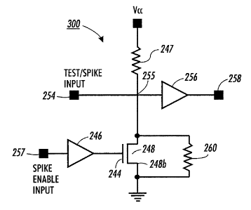
Fig. 2 illustrates one exemplary embodiment of the programmable previewable
circuit 200 according to this invention. The programmable previewable circuit
200
includes a spike enable input structure 257, a test and spike input structure
254, an
output structure 258, a pull-down transistor 248, an isolating input buffer
246 an
isolating output buffer 256 and a resistor 247. The output structure 258, the
test and
spike input structure 254, the pull-up resistor 247 and a first junction 248a
of the pull-
down transistor 248 are connected at a node 255. The other end of the resistor
247 is
connected to a voltage source 220 that applies a first predetermined voltage
to the
node 255 through the resistor 247. In contrast, the second junction 248b of
the pull-
down transistor 248 is connected to a "ground" voltage 230 that supplies a
second
predetermined value. When the transistor 248 is closed to connect the node 255
to the
ground voltage 230, the node 255 is driven to the second predetermined
voltage.
In the circuit 200, the spike enable input structure 257 is normally at a
voltage
level that places the pull-down transistor 248 into a default open, state.
This both
disconnects the node 255 from the ground and prevents the pull-down transistor
248
from being permanently set. External electronics can be applied to the test
and spike
input structure 254 to drive the output buffer 256 to a desired predetermined
voltage
value. In particular, the external test electronics can either not place a
voltage on the
test and spike input structure 254 or can place the first predetermined
voltage on the
test and spike input structure 254. As a result, the pull-up resistor 247
pulls the node
255 to the first predetermined voltage supplied by the voltage supply 220. In
contrast,
the external test electronics can place the second predetermined voltage
corresponding
to the ground voltage 230, on the test and spike input structure 254. As a
result, the
node 255 is pulled to the second predetermined voltage by the external test
electronics. The value of the output buffer 256 can then be read at the output
structure
258.
In order to permanently program the circuit 200, a large current is forced
through the transistor 248 by applying a signal to the spike enable input
structure 257
that closes the transistor 248. A higher voltage programming pulse train of
sufficient
amplitude, duration and frequency is applied to the test and spike input
structure 254.
The large potential across the transistor 248 between the voltage applied
through the
test and spike input structure 254 to the first junction 248a and the second
CA 02345570 2001-04-27
g
predetermined function applied by the ground voltage 230 to the second
junction 248b
causes the transistor 248 to go into snap back. This creates a very large
current
density through the functions 248a and 248b. This large current density causes
the
contacts on the junctions 248a and 248b to spike down through the junctions
248
creating a short circuit to the ground voltage 230, permanently removing the
resistor
247 and the voltage source 220 from the circuit 200.
The output structure 258 of the exemplary embodiment of the circuit 200 can
be coupled to a temperature controlled oscillator circuit 600 as shown in Fig.
6, such
that a grounded state or spiked state of the transistor 248 can be simulated
by applying
an input signal of the described levels to the test and spike input structure
254 while
the spike enable input structure 257 holds the transistor 248 in an open
state.
Consequently, the programmable previewable circuit according to this invention
is
capable of non-destructively simulating logical states of one or more
programmable
previewable elements of an electronic circuit.
Such programmable previewable circuits, however, are not limited to the
application of temperature controlled oscillator 600 but are also applicable
to any of
known or later developed circuit, including integrated circuits, that require
programming, circuits that enable functions such as logic network synthesis in
ASICs,
encoding or inscription of serial numbers, passwords, or electronic
"combination
lock" data, and storage of performance data in a product measured prior to
reaching an
end user require programming. In such circuits, whether or not a given
programmable
previewable circuit element is to be forced to a spiked condition or left at
its default
state is typically determined independently of the element itself.
For example, in programmable logic devices, a synthesized logic network is
realized by permanently setting or forcing to a known state the required
programmable
previewable circuit elements based on algorithms generated by a compiler. A
serial
number is a known digital quantity which is encoded into a device. A device's
measured output power can be represented by a digital quantity encoded in a
plurality
of programmable previewable circuit elements. In these cases, the typical
configuration of a fusible link circuit is described by a fuse element located
between a
ground node and a "blow" node as shown in the conventional circuit of Fig. 1.
In these
CA 02345570 2001-04-27
9
configurations, simulating a blown fuse is not possible since "normal" logic
voltage
applied to the input would destroy the fuse element.
The programmable previewable circuit according to this invention, however,
allows measurement or changes in a circuit's behavior to be observed by
applying the
first or second predetermined voltages to the circuit so long as the first and
second
predetermined voltages remain within the normal voltage levels for each
circuit. The
measured values of the circuit's behavior over the combinations of the
simulated states
can then be compared to a predetermined reference value. The combination of
programmed and default states for the various programmable previewable
antifuses
associated most closely with the desired reference output signal can be
permanently
written or programmed into a circuit by applying a close signal to particular
ones of
the spike enable input structures 257 to close the corresponding transistor
248 and by
applying higher programming voltages sufficient to cause spiking of the
metallic
contacts through the junction and into the substrate, but low enough to avoid
any
damage to the other circuit elements.
Once it has been determined that the desired output state to be generated at
the
output structure 258 requires the transistor 248 to be spiked, the spike
enable input
structure 257 is enabled and a programming voltage pulse train of sufficient
amplitude
and with peaks of sufficient duration and frequency is applied to the test and
spike
input structure 254 to cause the transistor 258 to spike. This input signal
should
include an amplitude which is low enough so as not to damage other elements in
the
circuit while being high enough to cause the transistor 248 to spike. The
spiking
causes a short circuit to ground at the junctions 248a and 248b.
Fig. 3 shows the physical changes that take place in the programmable
previewable circuit 200 as a result of enabling the spike enable input
structure 257
while placing the programming signal input pulse train of Fig. 5 , on the test
and spike
input structure 254. The resistive path 260 to the ground voltage 230 created
by
spiking the first junction 248a of the transistor 248 is shown in Fig. 3.
Fig. 4 illustrates a cross sectional view of one exemplary embodiment of the
pull-down transistor 248. In particular, Fig. 4 shows just the first junction
248a of the
transistor 248 after spiking. As shown in Fig. 4, the transistor 248 includes
a substrate
310, a junction 248a, which, in this exemplary embodiment of the transistor
248 is a
CA 02345570 2001-04-27
n+ region 320, an insulation layer 330 of silicon dioxide (Si02), and a
metallization
layer 340. The metallization layer 340 connects the junction 248a to the node
255. In
particular, the metallization layer 340 extends through a window formed on the
insulation layer 330 and contacts the n+ region 320. In various exemplary
5 embodiments of the metallization layer 340, usable in the programmable
previewable
circuit according to this invention, the metallization layer 340 comprises
aluminum
doped with 1 % silicon.
Before spiking, the n+ region 320 separates the metallization layer 340 from
the substrate 310. However, after spiking, a spike 350 of the material forming
the
10 metallization layer 340 extends through the n+ region 320 and into the
substrate 310.
As a result, the metallization layer 340 is permanently resistively connected
to the
substrate 310.
Fig. 5 shows one exemplary embodiment of a programming pulse train 500
that can be applied to the test and spike input structure of 254 to initiate
snap back in
the transistor 248 and thus spike the transistor 248. As shown in Fig. 5, the
pulse train
500 includes first - sixth pulses 510 - 560, separated by inter-pulse periods
515-555.
In general, during the pulses 510-560 a voltage of approximately 15V-20V is
applied
to the transistor 248 from the test and spike input structure 254. In
contrast, during
the inter-pulse periods 515-555, a voltage of approximately OV is applied to
transistor
248. However, depending on the design of the transistor 248, the voltage to be
applied during the pulses can be higher or lower, so long as the applied
voltage is
sufficient to spike the transistor 248.
The exemplary pulse train 500 includes six pulses 510-560. However, it
should be appreciated that the number, amplitude, duration and frequency of
the
pulses may be varied freely so long as the transistor 248 spikes without
damaging
other circuit elements of the chip.
The first pulse 510 of the exemplary embodiment is followed by an interpulse
period 515. The second pulse 520 is in turn followed by an interpulse period
525.
The first pulse 510 is 0.5 microseconds long while the first interpulse period
515 is 2
milliseconds long and the second pulse 520 is 0.4 microseconds long. The
remaining
pulses are 0.4 microseconds long while the other interpulse periods 525-555
are 2
milliseconds long. However, it should be appreciated that junctions composed
of
CA 02345570 2001-04-27
11
different compounds and different structures than those used in this exemplary
embodiment may be used, and that junctions composed of different compounds may
employ different voltage levels, pulse widths and interpulse widths. For
example,
CMOS junctions may be used in place of the NMOS junctions used in the
exemplary
embodiment of the transistor 248 described above.
In general, programming a programmable previewable circuit can be
accomplished using any type of signal that will induce spiking into the
particular type
of transistor used in the programmable previewable circuit according to this
invention.
Any type of transistor which can be spiked can be used in the programmable
previewable circuit according to this invention. Different types of transistor
fabrication techniques rnay be used. Furthermore, metallization layers
differing from
the exemplary metallization layer 340 containing 1 percent silicon, or
aluminum
copper combinations, may also be used. It should be appreciated that various
pulse
widths, frequencies and durations will be appropriate for different
metallization
layers, different circuit feature sizes and or different transistor
fabrication techniques,
and should be selected to ensure spiking while avoiding damaging other circuit
circuits in the chip.
Fig. 6 shows a tunable temperature controlled oscillator circuit 600 that
incorporates an exemplary embodiment of the programmable previewable circuit
according to this invention. The temperature controlled oscillator circuit 600
is
connected to first, second, third, fourth and fifth programmable previewable
circuits
692, 694, 696, 698, and 699.
An accessible test and spike input structure 602, 604, 606, 608, and 610, is
coupled, respectively, to each of the programmable previewable circuits 692,
694,
696, 698, and 699. Each of the test and spike input structures 602, 604, 606,
608, and
610 is coupled to one of the input structures of the programmable previewable
circuits
692-699. A common spike enable structure 611 is coupled to the spike enable
input
structures 257 of the programmable previewable circuits 692-699, for example,
spike
enable input structure 257 of Fig. 2.
The programmable previewable circuits 692-699 includes the output structures
258, which are coupled to the gates of the associated MOS transistors 6I2,
614, 616,
618, and 620, respectively. Each of the MOS transistors 612-620 is coupled to
an
CA 02345570 2001-04-27
12
associated capacitor 612-620. These five capacitors 612-620 are also coupled
to an
input 634 of a Schmitt trigger 632. An output signal on a trigger output 636
is
determined, at least in part, by the operable presence or absence of each of
the
capacitors 622, 624, 626, 628, and 630 on the tuneable temperature controlled
oscillator circuit 600. The operable states of the capacitor, 622-630 are
determined by
the simulated or actual states of the respectively associated programmable
previewable circuits 692-699.
The outputs of the programmable previewable circuits 692-699 can be
temporarily programmed by applying input signals to the corresponding
programmable previewable circuit input structures 254 to simulate the desired
output.
The programmable previewable circuits 692-699 can be permanently programmed by
applying an enable signal to the corresponding spike enable input structure
257.
The circuit 600 is designed to generate an output 640 signal having a
predetermined frequency that is indicative of the sensed temperature. However,
due
to the variations of integrated circuit fabrication, the signal provided at
the output 640
must be determined and tuned with respect to a predetermined reference signal.
Consequently, the signal provided at the output 640 may be adjusted by
applying five
input signals simultaneously to the inputs of the programmable previewable
circuits
692-699 and then varying these signals to generate a range of outputs that are
then
compared to the desired signal to be obtained at the output 640.
While this invention has been described in conjunction with a specific
embodiment thereof, it is evident that many alternatives, modifications, and
variations
will be apparent to those skilled in the art. For instance, this invention is
not limited
to the embodiments shown, but is applicable to any programmable previewable
circuit
useful for programming or establishing the output of an electronic circuit.
Accordingly, it is intended to embrace all such alternatives, modifications
and
variations that fall within the spirit and broad scope of the appended claims.