Language selection

Search

Patent 2345629 Summary

Third-party information liability

Some of the information on this Web page has been provided by external sources. The Government of Canada is not responsible for the accuracy, reliability or currency of the information supplied by external sources. Users wishing to rely upon this information should consult directly with the source of the information. Content provided by external sources is not subject to official languages, privacy and accessibility requirements.

Claims and Abstract availability

Any discrepancies in the text and image of the Claims and Abstract are due to differing posting times. Text of the Claims and Abstract are posted:

  • At the time the application is open to public inspection;
  • At the time of issue of the patent (grant).
(12) Patent Application: (11) CA 2345629
(54) English Title: VACUUM FIELD-EFFECT DEVICE AND FABRICATION PROCESS THEREFOR
(54) French Title: DISPOSITIF A EFFET DE CHAMP A VIDE ET PROCEDE DE FABRICATION
Status: Dead
Bibliographic Data
(51) International Patent Classification (IPC):
  • H01J 21/10 (2006.01)
  • H01J 9/02 (2006.01)
(72) Inventors :
  • POTTER, MICHAEL D. (United States of America)
(73) Owners :
  • ADVANCED VISION TECHNOLOGIES, INC. (United States of America)
(71) Applicants :
  • ADVANCED VISION TECHNOLOGIES, INC. (United States of America)
(74) Agent: SMART & BIGGAR
(74) Associate agent:
(45) Issued:
(86) PCT Filing Date: 2000-07-25
(87) Open to Public Inspection: 2001-02-01
Examination requested: 2001-03-26
Availability of licence: N/A
(25) Language of filing: English

Patent Cooperation Treaty (PCT): Yes
(86) PCT Filing Number: PCT/US2000/020230
(87) International Publication Number: WO2001/008193
(85) National Entry: 2001-03-26

(30) Application Priority Data:
Application No. Country/Territory Date
60/145,570 United States of America 1999-07-26
09/476,984 United States of America 1999-12-31
09/477,788 United States of America 1999-12-31

Abstracts

English Abstract


An ultra-high-frequency vacuum-channel field-effect microelectronic device
(VFED or IGVFED) has a lateral field-emission source (60), a drain (150), and
one or more insulated gates (40, 160). The insulated gate(s) are preferably
disposed to extend in overlapping alignment with the emitting edge (85) of the
lateral field-emission source and with a portion of the vacuum-channel region
(120). If the gate(s) are omitted, the device performs as an ultra-high speed
diode. A preferred fabrication process for the device uses a sacrificial
material temporarily deposited in a trench for the vacuum-channel region which
is covered with an insulating cover. An access hole in the cover allows
removal of the sacrificial material. As part of a preferred fabrication
process, the drain preferably acts also as a sealing plug, plugging the access
hole and sealing the vacuum-channel region after the vacuum-channel region is
evacuated.


French Abstract

La présente invention concerne un dispositif micro-électronique à effet de champ à canal de vide à fréquence ultra-haute (VFED ou IGVFED) comportant une source d'émission de champ latéral (60), un collecteur (150) et au moins une grille isolée (40, 160). Ces grilles isolées sont disposées de préférence de façon à se déployer en alignement de chevauchement avec le bord émetteur (85) de la source d'émission de champ latérale et avec une partie de la région du canal à vide (120). Si les grilles n'existent pas, le dispositif fonctionne comme une diode à très grande vitesse. Pour l'un des procédés de fabrication préférés du dispositif, on utilise un matériau sacrificiel déposé temporairement dans une tranchée pour la région du canal à vide qui est couverte d'une couverture isolante. Un trou d'accès dans la couverture permet l'élimination du matériau sacrificiel. Un aspect d'un procédé de fabrication préféré est de voir le drain agir de préférence également comme obturateur étanche, fermant le trou d'accès et obstruant de façon étanche la région du canal à vide une fois que la région du canal à vide a été évacuée.

Claims

Note: Claims are shown in the official language in which they were submitted.


CLAIMS

1. A vacuum field-effect device, comprising:
a) a source, said source comprising a lateral field-emitter, said lateral
field emitter
having an emitting, tip for emitting electrons,
said vacuum field-effect device being characterized by further comprising:
b) a drain spaced apart laterally from said emitting tip of said lateral field
emitter,
said drain comprising a conductive electrode;
c) a vacuum channel region disposed at least between said emitting tip of said
lateral field emitter and said drain;
d) at least one first gate, said at least one first gate comprising a
conductive
material being completely separated from said vacuum channel region by a
first insulating layer disposed between said at least one first gate and said
vacuum channel region to prevent any of said electrons emitted by said source
from reaching said at least one first gate; and
e) terminals for applying a bias voltage between said drain and said source
and
for applying a control signal to said at least one first gate.

2. The vacuum field-effect device of claim 1, further comprising an insulating
substrate, said lateral field-emitter of said source being disposed parallel
to said
insulating substrate.

3. The vacuum field-effect device of claim 2, wherein said insulating
substrate
comprises a material selected from the list consisting of glass, ceramic,
glass
ceramic, diamond, quartz, aluminum oxide, sapphire, silicon oxide, silicon
nitride, aluminum nitride, nickel oxide, plastic, polymer, polyimide,
parylene,
polyethylene terephthalate, and mixtures and combinations thereof.

-16-


4. The vacuum field-effect device of claim 1, wherein said first insulating
layer
comprises a material selected from the list consisting of glass, glass
ceramic,
quartz, aluminum oxide, sapphire, silicon oxide, silicon nitride, barium
strontium
titanate, titanium oxide, samarium oxide, yttrium oxide, tantalum oxide,
barium
titanium oxide, barium tantalum oxide, lead titanium oxide, strontium titanium
oxide, strontium (zirconium, titanium) oxide, aluminum nitride, polyimide,
parylene, and mixtures and combinations thereof.

5. The vacuum field-effect device of claim 1, wherein said first insulating
layer
comprises a material having an electric permittivity equal to or greater than
two.

6. The vacuum field-effect device of claim 1, wherein said at least one gate
is at
least partially aligned with said emitting tip of said lateral field emitter
and
disposed to be in at least partially overlapping alignment with said vacuum
channel region.

7. The vacuum field-effect device of claim 1, wherein said at least one gate
comprises a conductive material selected from the list consisting of aluminum,
copper, silver, gold, platinum, palladium, bismuth, conducting oxides,
conducting
nitrides, the refractory transition metals (titanium, vanadium, chromium,
zirconium, niobium, molybdenum, hafnium, tantalum, and tungsten), the
refractory transition metal carbides, the refractory transition metal
nitrides, boron
carbide, doped boron nitride, transition metal silicides, carbon in any of its
conductive forms (doped diamond, graphite, amorphous carbon, fullerenes,
nanotubes, or nanocoralline), silicon (N - type or P - type, polycrystalline,
amorphous, or single-crystal), germanium, and mixtures, alloys, and
combinations thereof.

8. The vacuum field-effect device of claim 1, wherein said lateral field-
emitter
comprises a thin-film conductor disposed on said first insulating layer.

9. The vacuum field-effect device of claim 8, further comprising a second
insulating
layer disposed over said thin film conductor.

-17-


10. The vacuum field-effect device of claim 9, wherein said second insulating
layer
comprises a material selected from the list consisting of glass, glass
ceramic,
quartz, aluminum oxide, sapphire, silicon oxide, silicon nitride, barium
strontium
titanate, titanium oxide, samarium oxide, yttrium oxide, tantalum oxide,
barium
titanium oxide, barium tantalum oxide, lead titanium oxide, strontium titanium
oxide, strontium (zirconium, titanium) oxide, aluminum nitride, polyimide,
parylene, and mixtures and combinations thereof.
11. The vacuum field-effect device of claim 9, wherein said second insulating
layer
comprises a material having an electric permittivity equal to or greater than
two.
12. The vacuum field-effect device of claim 9, wherein said first and second
insulating layers consist of the same insulating material.
13. The vacuum field-effect device of claim 1, further comprising at least one
second
gate, said at least one second gate being completely separated from said
vacuum
channel region by a third insulating layer disposed between said at least one
second gate and said vacuum channel region to prevent any of said electrons
emitted by said source from reaching said at least one second gate, and
further
comprising terminals for applying a control signal to said at least one second
gate.
14. The vacuum field-effect device of claim 13, wherein said at least one
second gate
is at least partially aligned with said emitting tip of said lateral field
emitter and
disposed to be in at least partially overlapping alignment with said vacuum
channel region.
15. The vacuum field-effect device of claim 13, wherein said at least one
second gate
comprises a conductive material selected from the list consisting of aluminum,
copper, silver, gold, platinum, palladium, bismuth, conducting oxides,
conducting
nitrides, the refractory transition metals (titanium, vanadium, chromium,
zirconium, niobium, molybdenum, hafnium, tantalum, and tungsten), the
refractory transition metal carbides, the refractory transition metal
nitrides, boron
carbide, doped boron nitride, transition metal silicides, carbon in any of its


-18-


conductive forms (doped diamond, graphite, amorphous carbon, fullerenes,
nanotubes, or nanocoralline), silicon (N - type or P - type, polycrystalline,
amorphous, or single-crystal), germanium, and mixtures, alloys, and
combinations thereof.
16. The vacuum field-effect device of claim 13, wherein said at least one
second gale
is at least partially aligned with said at least one first gate.
17. The vacuum field-effect device of claim 13, wherein said at least one
first gate
and said at least one second gate are aligned one with the other and are
disposed
symmetrically with each other about a plane through said source.
18. The vacuum field-effect device of claim 13, wherein said at least one
second gate
is spaced vertically apart from said source by a first predetermined spacing.
19. The vacuum field-effect device of claim 18, wherein said first
predetermined
spacing is between about one nanometer and about 1000 nanometers when the
electric permittivity of said second insulating layer is less than or equal to
20, and
said first predetermined spacing is between about 10 nanometers and about 5000
nanometers when the electric permittivity of said second insulating layer is
greater than 20.
20. The vacuum field-effect device of claim 13, wherein said at least one
first gate is
spaced vertically apart from said source by a second predetermined spacing.
21. The vacuum field-effect device of claim 20, wherein said second
predetermined
spacing is between about one nanometer and about 1000 nanometers when the
electric permittivity of said first insulating layer is less than or equal to
20, and
said second predetermined spacing is between about 10 nanometers and about
5000 nanometers when the electric permittivity of said first insulating layer
is
greater than 20.
22. The vacuum field-effect device of claim 20, wherein said at least one
second gate
is spaced vertically apart from said source by a spacing substantially equal
to said
second predetermined spacing.


-19-


23. The vacuum field-effect device of claim 13, wherein said first and second
gates
are electrically common, and said first and second control signals are common
to
said first and second gates.
24. The vacuum field-effect device of claim 1, wherein said source comprises a
conductive material selected from the list consisting of aluminum, copper,
silver,
gold, platinum, palladium, bismuth, conducting oxides, conducting nitrides,
the
refractory transition metals (titanium, vanadium, chromium, zirconium,
niobium,
molybdenum, hafnium, tantalum, and tungsten), the refractory transition metal
carbides, the refractory transition metal nitrides, boron carbide, doped boron
nitride, transition metal silicides, carbon in any of its conductive forms
(doped
diamond, graphite, amorphous carbon, fullerenes, nanotubes, or nanocoralline),
silicon (N - type or P - type, polycrystalline, amorphous, or single-crystal),
germanium, and mixtures, alloys, and combinations thereof.
25. The vacuum field-effect device of claim 1, wherein said drain comprises a
conductive material selected from the list consisting of aluminum, copper,
silver,
gold, platinum, palladium, bismuth, conducting oxides, conducting nitrides,
the
refractory transition metals (titanium, vanadium, chromium, zirconium,
niobium,
molybdenum, hafnium, tantalum, and tungsten), the refractory transition metal
carbides, the refractory transition metal nitrides, boron carbide, doped boron
nitride, transition metal silicides, carbon in any of its conductive forms
(doped
diamond, graphite, amorphous carbon, fullerenes, nanotubes, or nanocoralline),
silicon (N - type or P - type, polycrystalline, amorphous, or single-crystal),
germanium, and mixtures, alloys, and combinations thereof.
26. The vacuum field-effect device of claim 1, wherein said drain is spaced
apart
laterally from said emitting tip of said lateral field emitter by a spacing
between
about one manometer and about one millimeter.
27. A vacuum field-effect device, comprising:
a) an insulating substrate;
b) a first insulating layer;


-20-


c) a source, said source comprising a lateral field-emitter disposed parallel
to said
insulating substrate, said literal field-emitter comprising a thin-film
conductor
disposed on said first insulating layer, and said lateral field emitter having
an
emitting tip for emitting electrons;
d) a conductive drain spaced apart laterally from said emitting tip of said
lateral
field emitter, said conductive drain being disposed substantially
perpendicular
to said insulating substrate;
e) a vacuum channel region disposed at least between said emitting tip of said
lateral field emitter and said conductive drain, whereby electrons may move
unimpeded from said emitting tip of said lateral field emitter to said drain;
f) first and second gates, said first and second gates being completely
separated
from said vacuum channel region by second and third insulating layers
respectively disposed between said first and second gates and said vacuum
channel region to prevent any of said electrons emitted from said source from
reaching either of said first and second gates; and
g) terminals for applying a bias voltage between said drain and said source
and
for applying first and second control signals to said first and second gates
respectively.
28. The vacuum field-effect device of claim 27, wherein said insulating
substrate
comprises a conductive base substrate covered with an insulating surface
layer.
29. The vacuum field-effect device of claim 27, wherein said first and second
gates
are electrically common for applying said first and second control signals in
common to said first and second gates.
30. An ultra-high frequency vacuum diode device, comprising:
a) an insulating substrate;
b) a source, said source comprising a lateral field-emitter disposed parallel
to said
insulating substrate, said lateral field emitter having an emitting tip for
emitting electrons;


-21-


c) a drain spaced apart laterally from said emitting tip of said lateral field
emitter,
said drain comprising a conductive electrode;
d) a vacuum channel region disposed at least between said emitting tip of said
lateral field emitter and said drain; and
e) terminals for applying a voltage signal between said drain and said source.
31. An ultra-high frequency vacuum diode device, comprising:
a) an insulating substrate;
b) a first insulating layer;
c) a source, said source comprising a lateral field-emitter disposed parallel
to said
insulating substrate, said lateral field-emitter comprising a thin-film
conductor
disposed on said first insulating layer, and said lateral field emitter having
an
emitting tip for emitting electrons;
d) a conductive drain spaced apart laterally by a spacing between about one
nanometer and about one millimeter from said emitting tip of said lateral
field
emitter, said conductive drain being disposed substantially perpendicular to
said insulating substrate;
e) a vacuum channel region disposed at least between said emitting tip of said
lateral field emitter and said conductive drain, whereby electrons may move
unimpeded from said emitting tip of said lateral field emitter to said drain;
and
f) terminals for applying a voltage signal between said drain and said source
for
inducing a current of said electrons to flow directly from said source to said
conductive drain.
32. A process for fabricating a vacuum field-effect device, comprising the
steps of:
a) providing an insulating substrate;
b) forming a source by disposing a lateral field emitter parallel to said
substrate;
c) forming an emitting tip on said a lateral field emitter of said source;


-22-


d) providing a conductive drain spaced apart laterally from said emitting tip
of
said lateral field emitter for receiving electrons;
e) forming a first opening at least between said emitting tip of said lateral
field
emitter and said drain for a vacuum channel region;
f) disposing at least one first gate in at least partial alignment with
respect to said
emitting tip and in at least partially overlapping alignment with said first
opening;
g) substantially covering said first opening to form a closed vacuum channel
chamber;
h) removing any gases from said first opening to provide a vacuum therein; and
i) sealing said vacuum channel chamber.
33. The vacuum field-effect device made by the process of claim 32.
34. The process of claim 32, further comprising the step of:
j) disposing a first insulating layer between said at least one first gate and
said
vacuum channel region to prevent any of said electrons emitted by said source
from reaching said at least one first gate, said at least one first gate being
completely separated from said vacuum channel region by said first insulating
layer.
35. The process of claim 32, further comprising the step of:
k) forming terminals for applying a bias voltage between said drain and said
source and for applying a control signal to said at least one first gate.
36. The process of claim 32, wherein the step (a) of providing an insulating
substrate
is performed by providing a base substrate, said base substrate having any
degree
of conductivity or semiconductivity, and depositing an insulating layer on
said
base substrate.


-23-


37. The process of claim 32, wherein the steps (c) of forming an emitting tip
and (e)
of forming a first opening are performed together and substantially
simultaneously.
38. The process of claim 37, further comprising directionally etching at least
through
said lateral field emitter.
39. The process of claim 32, wherein the steps (d) of providing said
conductive drain
and (i) of sealing said vacuum channel chamber are performed together and
substantially simultaneously.
40. A process for fabricating a vacuum field-effect device, comprising the
steps of:
a) providing an insulating substrate;
b) forming a first trench in said insulating substrate;
c) filling said first trench with a first conductive layer for providing a
bottom gate
and planarizing;
d) depositing a first insulating layer over said insulating substrate and said
first
conductive layer for insulating said bottom gate;
e) depositing a second conductive layer and patterning to form a source layer
parallel to said substrate;
f) depositing a second insulating layer over said source layer;
g) forming a second trench for a vacuum channel region, while forming an
emitting tip of said source layer, thereby completing formation of a lateral
field emitter source;
h) filling said second trench with a sacrificial material and planarizing;
i) depositing a third insulating layer extending over said sacrificial
material;
j) forming an access hole through said third insulating layer to said
sacrificial
material;
k) forming openings for a source via and for a bottom gate via;


-24-


l) removing said sacrificial material through said access hole;
m) providing a vacuum environment; and
n) depositing and patterning a top gate, a conductive source contact, a bottom
gate contact, and a conductive drain, while sealing said vacuum channel
region, whereby said top gate is insulated by said third insulating layer from
said vacuum channel region.
41. The vacuum field-effect device made by the process of claim 40.
42. The process of claim 40, wherein the step (a) of providing an insulating
substrate
is performed by providing a base substrate, said base substrate having any
degree
of conductivity or semiconductivity, and depositing an insulating layer on
said
base substrate.
43. The process of claim 40, wherein said vacuum-environment-providing step
(m) is
performed by providing a vacuum pressure of less than or equal to about one
torr.
44. The process of claim 40, wherein said vacuum-environment-providing step
(m)
and said depositing and patterning step (n) are performed together and
substantially simultaneously.
45. The process of claim 40, wherein said insulating-substrate-providing step
(a)
comprises providing a substrate of an insulating material selected from the
list
consisting of glass, ceramic, glass ceramic, diamond, quartz, aluminum oxide,
sapphire, silicon oxide, silicon nitride, aluminum nitride, nickel oxide,
plastic,
polymer, polyimide, parylene, polyethylene terephthalate, and mixtures and
combinations thereof.
46. The process of claim 40, wherein said first-trench-forming step (b)
comprises
etching a recess into said insulating substrate.
47. The process of claim 46, wherein said first-trench-forming step (b)
comprises
directional etching with ions.
48. The process of claim 40, wherein said first-trench-filling step (c)
comprises filling
said first trench with a conductive material selected from the list consisting
of


-25-


aluminum, copper, silver, gold, platinum, palladium, bismuth, conducting
oxides,
conducting nitrides, the refractory transition metals (titanium, vanadium,
chromium, zirconium, niobium, molybdenum, hafnium, tantalum, and tungsten),
the refractory transition metal carbides, the refractory transition metal
nitrides,
boron carbide, doped boron nitride, transition metal silicides, carbon in any
of its
conductive forms (doped diamond, graphite, amorphous carbon, fullerenes,
nanotubes, or nanocoralline), silicon (N - type or P - type; polycrystalline,
amorphous, or single-crystal), germanium, and mixtures, alloys, and
combinations thereof.
49. The process of claim 40, wherein said first-insulating-layer depositing
step (d)
comprises depositing an insulating material selected from the list consisting
of
glass, glass ceramic, quartz, aluminum oxide, sapphire, silicon oxide, silicon
nitride, barium strontium titanate, titanium oxide, samarium oxide, yttrium
oxide, tantalum oxide, barium titanium oxide, barium tantalum oxide, lead
titanium oxide, strontium titanium oxide, strontium (zirconium, titanium)
oxide,
aluminum nitride, polyimide, parylene, and mixtures and combinations thereof.
50. The process of claim 40, wherein said first-insulating-layer depositing
step (d)
comprises depositing an insulating material having an electric permittivity
equal
to or greater than two.
51. The process of claim 40, wherein said second-conductive-layer depositing
and
patterning and source-layer-forming step (e) comprises depositing a conductive
material selected from the list consisting of aluminum, copper, silver, gold,
platinum, palladium, bismuth, conducting oxides, conducting nitrides, the
refractory transition metals (titanium, vanadium, chromium, zirconium,
niobium,
molybdenum, hafnium, tantalum, and tungsten), the refractory transition metal
carbides, the refractory transition metal nitrides, boron carbide, doped boron
nitride, transition metal silicides, carbon in any of its conductive forms
(doped
diamond, graphite, amorphous carbon, fullerenes, nanotubes, or nanocoralline),
silicon (N - type or P - type, polycrystalline, amorphous, or single-crystal),
germanium, and mixtures, alloys, and combinations thereof.


-26-


52. The process of claim 40, wherein said second-insulating-layer-depositing
step (f)
comprises depositing an insulating material selected from the list consisting
of
glass, glass ceramic, quartz, aluminum oxide, sapphire, silicon oxide, silicon
nitride, barium strontium titanate, titanium oxide, samarium oxide, yttrium
oxide, tantalum oxide, barium titanium oxide, barium tantalum oxide, lead
titanium oxide, strontium titanium oxide, strontium (zirconium, titanium)
oxide,
aluminum nitride, polyimide, parylene, and mixtures and combinations thereof.
53. The process of claim 40, wherein said second-insulating-layer-depositing
step (f)
comprises depositing an insulating material having an electric permittivity
equal
to or greater than two.
54. The process of claim 40, wherein said second-trench-forming step and
emitter-
tip-forming step (g) comprises directional etching with ions.
55. The process of claim 54, wherein said second-trench-forming and emitter-
tip-
forming step (g) further comprises plasma etching.
56. The process of claim 54, wherein said second-trench-forming and emitter-
tip-
forming step (g) further comprises wet etching.
57. The process of claim 40, wherein said second-trench-filling and
planarizing step
(h) comprises filling said second trench with an organic sacrificial material.
58. The process of claim 40, wherein said second-trench-filling and
planarizing step
(h) comprises filling said second trench with a sacrificial material selected
from
the list consisting of parylene, photoresist, wax, and silicon dioxide.
59. The process of claim 40, wherein said third-insulating-layer depositing
step (i)
comprises depositing an inorganic insulating material.
60. The process of claim 40, wherein said third-insulating-layer depositing
step (i)
comprises depositing an insulating material selected from the list consisting
of
glass, glass ceramic, quartz, aluminum oxide, sapphire, silicon oxide, silicon
nitride, barium strontium titanate, titanium oxide, samarium oxide, yttrium
oxide, tantalum oxide, barium titanium oxide, barium tantalum oxide, lead


-27-


titanium oxide, strontium titanium oxide, strontium (zirconium, titanium)
oxide,
aluminum nitride, polyimide, parylene, and mixtures and combinations thereof.
61. The process of claim 40, wherein said third-insulating-layer depositing
step (i)
comprises depositing an insulating material having an electric permittivity
equal
to or greater than two:
62. The process of claim 40, wherein said access-hole-forming step (j)
comprises
reactive ion etching through said third insulating layer to at least said
sacrificial
material.
63. The process of claim 40, wherein said sacrificial-material-removing step
(1)
comprises oxygen plasma etching through said access hole.
64. The process of claim 40, wherein said sacrificial-material-removing step
(1)
comprises dissolving said sacrificial material with a solvent.
65. The process of claim 40, wherein said sacrificial-material-removing step
(1)
comprises wet chemical etching through said access hole.
66. The process of claim 40, wherein said vacuum-environment-providing step
(m)
comprises providing a vacuum pressure less than or equal to about one torr.
67. The process of claim 40, wherein said depositing and sealing step (n)
comprises
the steps of:
o) depositing and patterning a top gate,
p) depositing and patterning a conductive source contact,
q) depositing and patterning a bottom gate contact,
r) depositing and patterning a conductive drain, and
s) sealing said vacuum channel region.
68. The process of claim 40, wherein said depositing and sealing step (n)
includes the
step of:
t) disposing said conductive drain spaced apart laterally from said emitting
tip of
said source layer.


-28-


69. The process of claim 40, further comprising the step of depositing a
passivation
layer over said device.
70. The process of claim 40, further comprising the steps of defining via-
openings
and depositing and patterning terminal metallurgy.
71. A process for fabricating an ultra-high frequency vacuum diode device,
comprising the steps of:
a) providing an insulating substrate;
b) forming a source by disposing a lateral field emitter parallel to said
substrate;
c) forming an emitting tip on said a lateral field emitter of said source;
d) providing a conductive drain spaced apart laterally from said emitting tip
of
said lateral field emitter for receiving electrons;
e) forming a first opening at least between said emitting tip of said lateral
field
emitter and said drain for a vacuum channel region;
f) substantially covering said first opening to form a closed vacuum channel
chamber;
g) evacuating said first opening; and
h) sealing said vacuum channel chamber.
72. The process of claim 71, wherein the step (a) of providing an insulating
substrate
is performed by providing a base substrate, said base substrate having any
degree
of conductivity or semiconductivity, and depositing an insulating layer on
said
base substrate.
73. A process for fabricating an ultra-high frequency vacuum diode device,
comprising the steps of:
a) providing an insulating substrate;
b) depositing a first insulating layer over said insulating substrate;
c) depositing a first conductive layer and patterning to form a source layer
parallel to said substrate;


-29-


d) depositing a second insulating layer over said source layer;
e) forming a trench for a vacuum channel region, while forming an emitting tip
of
said source layer, thereby completing formation of a lateral field emitter
source;
f) filling said trench with a sacrificial material and planarizing;
g) depositing a third insulating layer extending over said sacrificial
material;
h) forming an access hole through said third insulating layer to said
sacrificial
material;
i) forming an opening for a source via;
j) removing said sacrificial material through said access hole;
k) providing a vacuum environment; and
l) depositing and patterning a conductive source contact and a conductive
drain,
while sealing said vacuum channel region.
74. The vacuum field-effect device made by the process of claim 73.
75. The process of claim 73, wherein the step (a) of providing an insulating
substrate
is performed by providing a base substrate, said base substrate having any
degree
of conductivity or semiconductivity, and depositing an insulating layer on
said
base substrate.


-30-

Description

Note: Descriptions are shown in the official language in which they were submitted.


y4lAV 1~-Y~.~1~ CA 02345629 2001-03-26
t
Title of Invention
VACUUM FIELD-EFFECT DEVICE AND
FABRICATION PROCESS THEREFOR
Description
Technical Field
This invention relates to microelectronic devices and more particularly to a
vacuum-channel field-effect microelectronic device having a lateral field-
emission
source and preferably having insulated gate(s).
to This application is related to U.S. provisional application Serial No.
60/145,570 filed July 26, 1999, U.S. patent applications Serial Nos.
09/276,198 (now
U.S. Pat. No. 6,004,830), and 09/276,200, both filed March 25, 1999, and U.S.
patent
applications Serial Nos. 09/ 477,788 and 09/ 476,984, both filed December 13,
1999.
Nomenclature And Notations
Throughout this specification and the appended claims, the terms "lateral
emitter" or "lateral field-emission source" are used interchangeably to refer
to a field-
emission source disposed parallel to a substrate. For clarity and simplicity
of
expression, the terms "horizontal" and "vertical" are used herein to mean
parallel and
2o perpendicular to a substrate respectively, without implying any preferred
orientation
in space or any preferred orientation with respect to the earth's surface or
with respect
to the direction of a gravitational force. The acronyms "VFED" and "IGVFED"
are
used, referring to "vacuum field-effect device" and "insulated-gate vacuum
field-
effect device" respectively. The term "insulating," as in "insulating
substrate" or
"insulating layer," is used in its common meaning and particularly for
substances
characterized by a resistivity greater than 108 S2 - cm. The term "conductive"
refers
to substances characterized by a resistivity less than or equal to 108 S2 -
cm., i.e.,
including the resistivity range of both conductive and semiconductive
substances.


y'il H V 1-Yl.l CA 02345629 2001-03-26
r
Background Art
K. R. Shoulders described some vacuum integrated circuits in
"Microelectronics Using Electron-Beam-Activated Machining Techniques," in F.
L.
Alt (Ed.), "Advances in Computers," Vol. 2 (Academic Press, New York, 1961 )
pp.
135 - 197. An article, "Vacuum Integrated Circuits" by R. Greene et al.
(Technical
Digest of 1985 International Electron Devices Meeting [IEDM], IEEE,
Piscataway,
NJ, 1985, pp. 172 - 175), reviewed the physics and fabrication of vacuum
electronic
devices and showed a concept of a FET-like vacuum field emitter triode. The
field-
emission devices described by R. Greene et al. in that article required grid
biases of
to about 100 Volts and anode voltages of about 200 - 500 Volts. An article, "A
Vacuum
Field Effect Transistor Using Silicon Field Emitter Arrays" by Gray et al.
(Technical
Digest of 1986 International Electron Devices Meeting [IEDM], IEEE,
Piscataway,
NJ, 1986, pp. 776 - 779), described a vacuum field-effect transistor-like
device using
silicon field-emitter arrays. Another article by R. Greene et al., "Vacuum
Microelectronics, " (Technical Digest of 1989 International Electron Devices
Meeting
[IEDM], IEEE, Piscataway, NJ, 1989, pp. 89-15 - 89-19), described an
integrally
gridded field emitter array and an interdigitated silicon planar field emitter
array
vacuum FET.
An article by H. H. Busta et al., "Lateral Miniaturized Vacuum Device"
2o (Technical Digest of 1989 International Electron Devices Meeting [IEDM],
IEEE,
Piscataway, NJ, 1989, pp. 89-533 - 89-536), described two types of lateral
field
emitter triodes: one type with triangular shaped metallic emitters, a
collector
electrode, and an extraction electrode, and the other type with a tungsten
filament . v
emitter anchored to the sidewall of a polycrystalline silicon layer, a
collector
electrode, and an extraction electrode.
An article by W. J. Orvis et al., "A Progress Report on the Livermore
Miniature Vacuum Tube Project (Technical Digest of 1989 International Electron
Devices Meeting [IEDM], IEEE, Piscataway, NJ, 1989, pp. 89-529 - 89-531),
-2-


-' ' ' - ' ' - CA 02345629 2001-03-26
R a
described methods of making miniature vacuum diodes and triodes with Spindt-
type
field emitters. The triodes of Orvis et al. had free-standing anodes and
grids.
An article by J. E. Cronin et al., "Field Emission Triode Integrated-Circuit
Construction Method," IBM Technical Disclosure Bulletin, Vol. 32, No. SB (Oct.
1989) pp. 242-243, described a process for fabrication of field-emission
triodes
having field-emission tips self aligned to a control grid.
An article by B. Goodman, "Return of the Vacuum Tube," Discover, March
1990, pp. 55 - 58, described progress and problems in development of vacuum
microelectronics. An article by S. Kanemura et al., "Fabrication and
Characterization
of Lateral Field Emitter Triodes," IEEE Transactions on Electron Devices, Vol.
38,
No. 10, Oct. 1991, pp. 2334 - 2336, described lateral field-emitter triodes
having an
array of 170 field-emitter tips with a 10-micrometer pitch, a columnar gate,
and an
anode.
An article by W. N. Carr et al., "Vacuum Microtriode Characteristics," J. Vac.
Sci. Technol., Vol. A8 (4), July/Aug 1990, pp. 3581 - 3585, described pentode-
like
I-V characteristics simulated for lateral vacuum microelectronic devices with
wedge-
shaped field-emission cathodes.
An article by A. A. G. Driskill-Smith et al., "The 'Nanotriode:' A Nanoscale
Field-Emission Tube," Applied Physics Letters, Vol. 75 No. 18 (Nov. 1, 1999),
pp.
2845 - 2847, described a nanoscale electron tube with a field-emission cathode
(vertical metal "nanopillars" with radii of about one nanometer), an
integrated anode,
and a control gate, all within vertical and horizontal dimensions of about 100
nm. An
article by P. Weiss, "Vacuum Tubes' New Image: Too Small to See," in Science
News, Vol. 156 (Nov. 6, 1999), summarized the vacuum tube development of
Driskill-Smith et al. and reports some comments of others skilled in this
field. An
article, "Vacuum Tubes Attempt a Comeback," in Physics Today, Dec. 1999, p. 9,
summarized some advantages of the vertically oriented devices of the Driskill-
Smith
et al. article and some remaining problems with that device design.
-3-


941 AVT-PCT
CA 02345629 2001-03-26
c
Many prior U.S. patents have described vacuum microelectronic devices
(especially field-emission devices) and their fabrication processes, including
3,753,022 to Fraser, Jr.; 3,755,704 and 3,789,471 to Spindt et al.; 4,163,949
to
Shelton; 4,578,614 to Gray et al.; 4,721,885 to Brodie; 4,827,177 to Lee;
4,983,878
to Lee et al.; 5,007,873 to, Goronkin et al.; 5,012,153 to Atkinson et al.;
5,070,282 to
Epsztein; 5,079,476 to Kane; 5,112,436 to Bol; 5,126,287 to Jones; 5,136,764
to
Vasquez; 5,144,191 to Jones et al.; 5,214,347 to Gray; 5,221,221 to Okaniwa;
5,245,247 and 5,267,884 to Hosogi; 5,268,648 to Calcatera; 5,270,258 and
5,367,181 to Yoshida; 5,394,006 to Liu; 5,493,177 to Muller et al.; and
5,834,790
1o and 5,925,975 to Suzuki.
A number of prior U.S. patents have described microelectronic device
structures with lateral field-emission cathodes and fabrication processes for
such
structures, including Lee 4,827,177; Bol 5,112,436; Jones, et. al. 5,144,191;
Gray
5,214,347; Cronin et al. 5,233,263, 5,308,439, 5,312,777, and 5,530,262; Xie
et al.
5,528,099; Mandelman et al. 5,604,399, 5,629,580, 5,736,810, and 5,751,097;
and
Potter 5,616,061, 5,618,216, 5,628,663, 5,630,741, 5,644,188, 5,644,190,
5,647,998, 5,666,019, 5,669,802, 5,691,599, 5,700,176, 5,703,380, 5,811,929,
5,831,384, 5,850,123, 5,872,421, 5,920,148, 5,965,192, 6,004,830, 6,005,335,
6,015,324, 6,015,326, 6,017,257, 6,037,708, and 6,071,633.
2o There is a continuing need for ultra-high-frequency electronic devices. At
present, many of the needs for ultra-high frequency devices are met by
semiconductor
devices and integrated circuits. Since electron mobilities in semiconductor
devices
are reduced by carrier collisions with atoms of the crystal lattice, the
potentially better
high-frequency performance of miniature vacuum devices is attractive. Such
vacuum
devices, if made small enough and capable of operating at low-enough voltages,
with
sufficiently high and stable currents, will find a wide range of electronics
applications,
both digital and analog.
-4-


941 AVT-PCT
Disclosure of Invention
CA 02345629 2001-03-26
S o
An ultra-high-frequency vacuum-channel field-effect microelectronic device
(VFED or IGVFED) has a lateral field-emission source, a drain, and one or more
insulated gates. The insulated gates) is preferably disposed to extend in
overlapping
alignment with the emitting edge of the lateral field-emission source and with
a
portion of the vacuum channel region. If the gates) is omitted, the device
performs as
an ultra-high-speed diode. A preferred fabrication process for the device uses
a
sacrificial material temporarily deposited in a trench for the vacuum channel
region,
which is covered with an insulating layer cover. An access hole in the cover
allows
io removal of the sacrificial material. As part of a preferred fabrication
process, the
drain preferably acts also as a sealing plug, plugging the access hole and
sealing the
vacuum-channel region after the vacuum-channel region is evacuated.
Brief Description of Drawings
FIG. 1 is a partially cut-away perspective view of an insulated-gate vacuum
field-effect device made in accordance with the invention.
FIGS. 2a - 2 j are side-elevation cross-sectional views of the device in
various
stages of a preferred fabrication process.
FIG. 3 is a flowchart illustrating the steps of a preferred fabrication
process
performed in accordance with the invention.
2o Modes for Carrying Out the Invention
Disclosed herein is a new ultra-high-switching-speed vacuum field-effect
device (VFED). The charge carrier source for the VFED is an electron emitter
source
operable via Fowler-Nordheim emission. The channel region is a vacuum. Since
there is no material in the channel region to scatter the electrons and the
channel
length is short, the electron transit time is very short. There is no vacuum
path
between the source and gate or between the drain and gate. Therefore, a
relatively
high drain potential can be maintained without causing electron emission from
the
-5-


941AVT-PCT
CA 02345629 2001-03-26
gate. The high drain potential together with the short vacuum channel leads to
an
electron transit time on the order of sub-picoseconds. Furthermore, taking
into
account the very small parasitic capacitance terms (sub-
femtofarads/micrometer) of
the new VFED, in-depth calculations predict switching speeds up to 10
terahertz for a
0.5 micrometer vacuum channel length. For a 0.1 micrometer vacuum channel
length,
the calculated speed of the device is nearly 30 terahertz.
For applications where it is desirable to minimize the output impedance,
(rp = 8Vd/8Id @ Vg = constant), a very short vacuum channel length will allow
a
significant change in drain current due to the drain's potential influence on
the source
1o field. Here, Vd is the drain voltage, Id is the drain current, and Vg is
the gate voltage.
Furthermore, a number of individual devices arranged to be electrically in
parallel will
reduce the effective output impedance without diminishing switching speed. The
transconductance, (gm = 8Id/8Vg @ Vd = constant), can be high due to the
effective
close proximity of the gate to the source. The use of high dielectric-constant
insulators can aid the gate influence; however, the consideration of
increasing the gate
to source parasitic capacitance should be taken into account. The electric
permittivity
preferably has a value greater than two. The gain parameter, ( ~t = ~ 8Vd/8Vg
( @ Id
= constant), can be large due to the strong influence of the gate on the
channel current
with a vacuum channel length in the range of about equal to or greater than
0.5
micrometer.
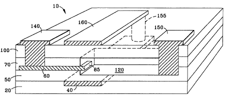
FIG. 1 (not to scale) is a partially cut-away perspective view of an insulated-

gate vacuum-channel field-effect device 10 made in accordance with the
invention.
Device 10 is made on an insulating substrate 20. Source layer 60 (a lateral
field-
emission cold cathode with emitting tip 85) is parallel to substrate 20. While
FIG. 1
and the cross-section drawings 2f - 2 j show emitting tip 85 schematically as
having a
rectangular shape, the actual shape of the emitting tip 85 can be a very sharp
edge ,
i.e., an extremely small radius, as is known in the art of field-emission
cathodes. A
drain 150 collects electrons emitted from emitting tip 85 of source 60 when a
suitable
bias voltage is applied to source 60 and drain 150. Drain 150 is spaced apart
laterally
from emitting tip 85 of the source 60 by a spacing preferably between about
one
-6-


941 AVT-PCT
CA 02345629 2001-03-26
nanometer and about one millimeter. Gates, preferably bottom gate 40 and top
gate
160, are disposed in at least partial alignment with emitting edge 85 of
source 60 and
extend to overlap a portion of a vacuum-channel region 120. A conductive
bottom-
gate contact 155 extends down and makes ohmic electrical contact with bottom
gate
40. Contact 155 is also connected to top gate 160 in the embodiment shown in
FIG.
1. The use of a recess in substrate 20 for bottom gate 40 allows for
planarization of
gate 40 and therefore provides for precise control and uniformity of the
thickness of
insulating layer 50 deposited over gate 40 in a preferred fabrication process,
described
in detail below. However, in other embodiments, gate 40 may be disposed on the
top
surface of substrate 20, without a recess.
An insulating layer between each gate and the vacuum channel region prevents
any electrons emitted by the source from reaching either gate, each gate being
completely separated from the vacuum channel region by its respective
insulating
layer (50 or combination of 70 with 100). Each of these insulating layers also
prevents any vacuum path between its corresponding gate and the drain 150, so
there
is no possibility of electron current flowing through the vacuum between
either gate
and the drain (for example, secondary electron current). It will be understood
that this
is also true for an IGVFED having only one gate instead of the two-gate
preferred
embodiment described and illustrated herein. In the embodiment of FIG. 1,
which has
2o two gates, the conductive contact 155 that interconnects them is also fully
insulated
from vacuum-channel region 120 by the insulators 50, 70, and 100. As shown in
FIG.
1, the dimensions of vacuum-channel region 120 are designed to prevent vacuum-
.
channel region 120 from extending back to the region of conductive contact
155.
A conventional passivation layer (not shown) may be deposited over device 10
to protect the device and to prevent surface leakage currents. Conventional
via-
openings may be formed and conventional terminal metallurgy (not shown) may be
deposited to contact the conductive elements shown in FIG. 1.
Thus, one aspect of the invention is a vacuum field-effect device 10 having a
source 60 comprising a lateral field-emitter with an emitting tip 85 for
emitting


941AVT-PCT
CA 02345629 2001-03-26
electrons, having a conductive drain 150 spaced apart laterally from the
emitting tip,
having a vacuum channel region 120 extending at least between the emitting tip
85 of
the source and the drain 150, having at least one gate 40 or 160, completely
separated
from the vacuum channel region by an insulating layer 50, 70, or 100 disposed
between the gate and the vacuum channel region 120 to prevent any electrons
emitted
by the source from reaching the gate, and having terminals (e.g., 140) for
applying a
bias voltage between the drain and source and for applying a control signal to
the gate.
The terminals may be integral with their respective electrodes, such as 150
and 160 in
FIG. 1. The device preferably has two electrically common gates 40 and 160,
which
to may be connected by an integrated conductive gate contact 155. The device
is
constructed on an insulating substrate Z0, which may consist of an insulating
film on a
conductive or semiconductive substrate.
Fabrication Process
The new terahertz vacuum field-effect device (VFED) is much simpler to
fabricate than compound semiconductor or heterojunction semiconductor devices.
No
semiconductor materials are used in the preferred embodiment. The structure
fabrication is, however, compatible with standard IC metallization,
passivation, and
interconnecting processing. Furthermore, the new device can be integrated with
either
variations of the preferred embodiment fabrication process or with other
integrated-
2o circuit fabrication processes.
An overall process for fabricating the vacuum field-effect device includes the
steps of providing a suitably flat insulating substrate, forming a source by
disposing a
lateral field emitter parallel to the substrate, forming an emitting tip on
the lateral field
emitter of the source, providing a conductive drain spaced apart laterally
from the
emitting tip for receiving electrons, forming a first opening for a vacuum
channel
region at least between the emitting tip and the drain, disposing at least one
gate in at
least partial alignment with respect to the emitting tip and in at least
partially
overlapping alignment with the first opening, substantially covering the first
opening
to form a closed vacuum channel chamber, removing any gases from the first
opening
3o to provide a vacuum, and sealing the vacuum channel chamber. The overall
process
_g_


941AVT-PCT ~ 02345629 2001-03-26
s ,
may also include the step of disposing an insulating layer between the gate
and the
vacuum channel region to prevent any of the electrons emitted by the source
from
reaching the gate, the gate being completely separated from the vacuum channel
region by the insulating layer. Terminals are added for applying a bias
voltage
between the source and drain and for applying a control signal to the gate.
The step of providing an insulating substrate may be accomplished by first
providing a base substrate, where the base substrate may have any degree of
conductivity or semiconductivity, and then depositing an insulating surface
layer on
the base substrate. Thus the base substrate may be a conductor, a
semiconductor, or
to any substance characterized by a resistivity of less than about 108 S2-cm.,
or an
insulator differing in composition from the insulating layer deposited on it.
For
example, the base substrate may be a metal, silicon, germanium, III-V
compounds
(GaAs, AIGaAs, InP, GaN, etc.), conducting oxides (e.g., indium tin oxide,
indium
oxide, tin oxide, copper oxide, or zinc oxide), transition metal nitrides, or
transition
metal carbides.
Within the framework of this overall fabrication process, many variations of
particular materials and specific process methods and their sequence may be
made.
The following description, read in conjunction with FIGS. 2a - 2 j and 3,
gives details
of a particularly preferred fabrication process. FIGS. 2a - 2 j are not drawn
to scale.
This description includes steps for providing two gates, but it will be
recognized that a
VFED device may be made with one or more gates and that the gates may be
omitted
to make a high-speed diode.
FIGS. 2a - 2j show a series of side-elevation cross-sectional views showing
the results of specific steps of the preferred process. FIG. 3 shows a flow
chart
representing the preferred fabrication process, in which steps are designated
by
reference numerals Sl, ..., S21. For each of these steps, the act performed is
listed in
Table I (following page). '
-9-


941AVT-PCT ~ 02345629 2001-03-26
r
S1 Provide substrate


S2 Form a first trench


S3 Fill first trench with conducting layer and planarize


S4 Deposit first insulating layer


SS Deposit conductive material and pattern source


S6 Deposit second insulating layer


S7 Form second trench to define vacuum channel region ,


S8 Fill second trench with sacrificial material and planarize


1o S9 Deposit third insulating layer


S10 Form access hole through third insulating layer


S11 Form source via and bottom gate via openings


S12 Remove sacrificial material


S13 Provide vacuum environment


S14 Deposit and pattern conductive source contact


S15 Deposit and pattern conductive top gate


S16 Deposit and pattern conductive bottom gate contact


S17 Deposit and pattern conductive drain


S18 Seal vacuum-channel region
2o S19 (Combination of steps S14 through S18 performed together
simultaneously)
S20 If desired, deposit passivation
S21 If desired, form via holes and tenminal metallurgy
TABLE I. Process steps of FIG. 3
In step S1, a suitably flat insulating substrate 20 is provided. Insulating
substrate 20 may comprise any suitable insulating material such as glass,
ceramic,
glass ceramic, diamond, quartz, aluminum oxide, sapphire, silicon oxide,
silicon
nitride, aluminum nitride, nickel oxide, plastic, polymer, polyimide,
parylene,
- 10-


941AVT-PCT ~ 02345629 2001-03-26
polyethylene terephthalate, and mixtures and combinations thereof. As
mentioned
above, the flat insulating substrate 20 provided in step S1 may be made by
first
providing a conductive base substrate, such as a silicon semiconductor wafer,
and
depositing a surface layer of a suitable insulating material on the conductive
base
substrate to form an insulating surface. The insulating layer may be any of
the
insulating materials listed above, for example.
In step S2, a trench 30 is formed in the surface of the insulating substrate
(FIG.
2a). In step S3, trench 30 is filled with a conducting layer 40 and planarized
(FIG. 2b)
to form a first gate. The planarization may be done by chemical-mechanical
polishing
to (CMP). Some suitable materials for conducting layer 40 are aluminum,
copper, silver,
gold, platinum, palladium, bismuth, conducting oxides, conducting nitrides,
the
refractory transition metals (titanium, vanadium, chromium, zirconium,
niobium,
molybdenum, hafnium, tantalum, and tungsten), the refractory transition metal
carbides, the refractory transition metal nitrides, boron carbide, doped boron
nitride,
transition metal silicides, carbon in any of its conductive forms (e.g., doped
diamond,
graphite, amorphous carbon, fullerenes, nanotubes, or nanocoralline), silicon
(N - type
or P - type, polycrystalline, amorphous, or single-crystal), germanium, and
mixtures,
alloys, and combinations thereof. The conductive material is chosen to be
compatible
in processing with the other materials of the device.
Step S4 consists of depositing a first insulating layer 50 over the planarized
surface (FIG. 2c). First insulating layer 50 may comprise any suitable
insulator, such
as glass, glass ceramic, quartz, aluminum oxide, sapphire, silicon oxide,
silicon
nitride, barium strontium titanate, titanium oxide, samarium oxide, yttrium
oxide,
tantalum oxide, barium titanium oxide, barium tantalum oxide, lead titanium
oxide,
strontium titanium oxide, strontium (zirconium, titanium) oxide, aluminum
nitride,
polyimide, parylene, or mixtures and combinations thereof. The electric
permittivity E
of first insulating layer 50 preferably has a value greater than two.
In step S5, a conductive material is deposited and patterned to define a
source
layer 60 (FIG. 2d). In step S6, a second insulating layer 70 is deposited,
covering the
source layer 60 (FIG. 2e). Second insulating layer 70 may comprise any
suitable
-11-


941 AVT-PCT
CA 02345629 2001-03-26
insulator, such as any of the materials used for first insulating layer 50
(glass, glass
ceramic, quartz, aluminum oxide, sapphire, silicon oxide, silicon nitride,
barium
strontium titanate, titanium oxide, samarium oxide, yttrium oxide, tantalum
oxide,
barium titanium oxide, barium tantalum oxide, lead titanium oxide, strontium
titanium
oxide, strontium (zirconiu;n, titanium) oxide, aluminum nitride, polyimide,
parylene,
or mixtures and combinations thereof). However, it is preferable that
insulating layers
50 and 70 consist of the same insulating material. The electric permittivity s
of
second insulating layer 70 preferably has a value greater than two.
A second trench 80 for a vacuum channel region is formed (step S7, FIG. 2f)
by etching at least through second insulating layer 70 and source layer 60,
but not
down as far as first gate layer 40. Trench 80 may be formed by directional
reactive
ion etching. Forming this trench also etches source layer 60 to form emitting
tip 85.
If necessary, further etching, such as an isotropic wet etch or plasma etch
may be used
to further etch emitting tip 85. As is known in the art of field-emission
cathodes, it is
desirable to form emitting edge 85 with an extremely small radius, to have a
very
sharp knife-edge shape. This is accomplished by depositing a very thin source
layer
60 in step S5, and then by etching the thin layer's edge in step S7. Suitable
conductive materials for source layer 60 are aluminum, copper, silver, gold,
platinum,
palladium, bismuth, conducting oxides, conducting nitrides, the refractory
transition
2o metals (titanium, vanadium, chromium, zirconium, niobium, molybdenum,
hafnium,
tantalum, and tungsten), the refractory transition metal carbides, the
refractory
transition metal nitrides, boron carbide, doped boron nitride, transition
metal silicides,
carbon in any of its conductive forms (e.g., doped diamond, graphite,
amorphous
carbon, fullerenes, nanotubes, or nanocoralline), silicon (N - type or P -
type,
polycrystalline, amorphous, or single-crystal), germanium, and mixtures,
alloys, and
combinations thereof. As is well known in the art, it is preferable to use a
material of
low work function, at least at emitting edge 85 of source layer 60.
In step S8, second trench 80 is filled with a sacrificial material 90 and
planarized (FIG. 2g). Sacrificial material 90 may be an inorganic material or
an
organic material such as parylene. A third insulating layer 100 is deposited
(step S9,
-12-


941AVT-PCT ~ 02345629 2001-03-26
FIG. 2h). Third insulating layer 100 may comprise any suitable insulator, such
as any
of the materials used for first insulating layer 50 and second insulating
layer 70.
Insulating layer 100 preferably consists of the same insulating material as
insulating
layers 50 and 70 and preferably has an electric permittivity s of greater than
two.
In step S10, an access hole I10 is opened through third insulating layer 100
down at least into sacrificial material 90 (FIG. 2i). Access hole 110 is
preferably
made at or near the edge of trench 80 that is spaced farthest from emitting
tip 85. In
step S11, source via-opening 130 and a via-opening (not shown) for bottom gate
40
are formed. The bottom gate contact 155 (shown in FIG. 1) uses this bottom
gate via-
opening, which is out of the plane of the cross-sections of FIGS. 2a - 2j.
Optionally,
steps S10 and S11 may be combined and performed simultaneously, as indicated
in
FIG. 3 by a bracket joining these two steps. In step S12, sacrificial material
90 is
removed through access hole 110, e.g., by dissolving sacrificial material 90
with a
suitable solvent and removing the solution through access hole 110. For
example, if
the sacrificial material 90 is photoresist or wax, the solvent may be acetone.
If the
sacrificial material 90 is silicon dioxide, it may be removed by wet chemical
etching,
e.g., with HF. For many sacrificial materials, the removal process may be done
by
oxygen plasma etching. Removing the sacrificial material leaves an empty
vacuum
channel region 120. The next few steps may be performed in a vacuum
environment,
with a vacuum pressure preferably less than or equal to about one tort,
provided in
step S13.
In step S 14, a conductive source contact 140 is deposited and patterned. In
step S15, a conductive top gate 160 is deposited and patterned. In step S16, a
conductive bottom gate contact 155 (shown in FIG. 1) is deposited and
patterned. In
step S17, a conductive drain 150 is deposited and patterned. Suitable
conductive
materials for conductive top gate 160, conductive bottom gate contact 155, and
conductive drain 150 are aluminum, copper, silver, gold, platinum, palladium,
bismuth, conducting oxides, conducting nitrides, the refractory transition
metals
(titanium, vanadium, chromium, zirconium, niobium, molybdenum, hafnium,
tantalum, and tungsten), the refractory transition metal carbides, the
refractory
-13-


941AVT-PCT ~ 02345629 2001-03-26
transition metal nitrides, boron carbide, doped boron nitride, transition
metal silicides,
carbon in any of its conductive forms (e.g., doped diamond, graphite,
amorphous
carbon, fullerenes, nanotubes, or nanocoralline), silicon (N - type or P -
type,
polycrystalline, amorphous, or single-crystal), germanium, and mixtures,
alloys, and
combinations thereof.
In step S18, access hole 110 is filled to seal the vacuum channel region 120.
This step S18 is preferably performed at a vacuum pressure of less than or
equal to
about one torr. When the vacuum channel region 120 is sealed, the channel
region
will be at vacuum. Steps S14 - S18 are preferably all performed together
simultaneously as a step S19, as indicated in Fig. 3 by a bracket. In this
preferred
process, access hole 110 also defines the pattern for the lower part of drain
150 (inside
vacuum chamber channel region 120). The resultant device after performing
steps
S14 - S18 or the combined step S19 is shown in the cross-sectional view of
FIG. 2j
and in the partially cut-away perspective view of FIG. 1. Alternatively to
this process,
forming conductive drain 150 and sealing vacuum channel region 120 may be
accomplished by the methods of U.S. Pat. No. 5,700,176 to Potter, the entire
disclosure of which is incorporated herein by reference. If desired, a
passivation layer
may be deposited (step S20) and via-openings formed and terminal metallurgy
deposited (step S21).
2o A person skilled in the art will recognize that simply by omitting those
process
steps for incorporating control gate elements 40 and 160, an ultra-high
frequency
diode structure is realized. If one of the control gate elements 40 and 160 is
omitted,
and the other included, the device will still operate as a triode.
The vacuum field-effect device of this invention may be made with very wide
ranges of dimensions and of material characteristics such as electric
permittivity of
insulators. For example, depending on the application, the vacuum channel
length
may be made between about one nanometer and about one millimeter. There are
wide
ranges of electric permittivities s, drain voltage values, tradeoffs with
coupling
capacitance, and enhancement vs. retardation mode of operation. The
thicknesses of
the insulating layers 50 and combination of 70 and 100 (i.e., the spacing of
the gates
-14-


941AVT-PCT CA 02345629 2001-03-26
from source layer 60) is preferably chosen to be between about one nanometer
and
about 1000 nanometers when the electric permittivity of the insulating layer
is less
than or equal to 20, and the spacing is preferably chosen to be between about
10
nanometers and about 5000 nanometers when the electric permittivity of the
insulating layer is greater than 20.
Industrial Applicability
The device disclosed herein is particularly useful for high bandwidth
communication requirements. Such uses of the device include transmitting and
receiving data at the chip level, and thus, the device is suitable for short-
range intra-
LAN communication, wired or wireless. The device also inherently has high
thermal
tolerance and radiation resistance. It is therefore desirable for applications
in harsh
environments. These applications include sensor applications for fission or
fusion
reactors, borehole sensors, accelerator sensors and instrumentation,
applications in
satellites, deep space and extraterrestrial exploration vehicles, and many
other similar
applications.
Other embodiments of the invention to adapt it for various uses and conditions
will be apparent to those skilled in the art from a consideration of this
specification or
from practice of the invention disclosed herein. For example, additional gate
electrodes may be incorporated into the structures. For another example, the
device
2o may be fabricated on an insulating substrate comprising a suitable plastic
or other
polymer, which may be flexible and/or transparent, or conductive elements may
be
made of conductive polymers. Also, the order of the various fabrication
process steps ,
may be varied for some purposes, and some process steps may be omitted for
fabrication of the simpler structures. It is intended that the specification
and examples
be considered as exemplary only, with the true scope and spirit of the
invention being
defined by the following claims.
What is claimed is:
-15-

Representative Drawing
A single figure which represents the drawing illustrating the invention.
Administrative Status

For a clearer understanding of the status of the application/patent presented on this page, the site Disclaimer , as well as the definitions for Patent , Administrative Status , Maintenance Fee  and Payment History  should be consulted.

Administrative Status

Title Date
Forecasted Issue Date Unavailable
(86) PCT Filing Date 2000-07-25
(87) PCT Publication Date 2001-02-01
(85) National Entry 2001-03-26
Examination Requested 2001-03-26
Dead Application 2003-07-25

Abandonment History

Abandonment Date Reason Reinstatement Date
2002-07-25 FAILURE TO PAY APPLICATION MAINTENANCE FEE

Payment History

Fee Type Anniversary Year Due Date Amount Paid Paid Date
Application Fee $150.00 2001-03-26
Registration of a document - section 124 $100.00 2001-03-26
Request for Examination $200.00 2001-03-26
Owners on Record

Note: Records showing the ownership history in alphabetical order.

Current Owners on Record
ADVANCED VISION TECHNOLOGIES, INC.
Past Owners on Record
POTTER, MICHAEL D.
Past Owners that do not appear in the "Owners on Record" listing will appear in other documentation within the application.
Documents

To view selected files, please enter reCAPTCHA code :


To view images, click a link in the Document Description column. To download the documents, select one or more checkboxes in the first column and then click the "Download Selected in PDF format (Zip Archive)" or the "Download Selected as Single PDF" button.

List of published and non-published patent-specific documents on the CPD .

If you have any difficulty accessing content, you can call the Client Service Centre at 1-866-997-1936 or send them an e-mail at CIPO Client Service Centre.


Document
Description 
Date
(yyyy-mm-dd) 
Number of pages   Size of Image (KB) 
Representative Drawing 2001-06-26 1 12
Abstract 2001-03-26 1 23
Description 2001-03-26 15 731
Claims 2001-03-26 15 634
Drawings 2001-03-26 4 86
Cover Page 2001-06-26 1 44
Assignment 2001-03-26 5 266
PCT 2001-03-26 2 92