Note: Descriptions are shown in the official language in which they were submitted.
CA 02346361 2001-04-06
WO 00/21130 PCT/US99/22606
-1
METHODS AND .APPARATUS FOR HERMETICALLY SEALING
ELECTRONIC PACKAGES
BACKGROUND OF THE INVENTION
The United States Government has acquired certain rights in this invention
pursuant to Contract No. N00024-98-2-4022 awarded by the United States
Department
of the Navy.
1. Field of the Invention
to The present invention generally relates to methods and apparatus for
component
packaging and more particularly to systems for sealing opto-electronic
components
within standard chip packages.
2. Description of the Related Art
The use of opto-electronic components, such as laser diodes, photodetectors,
and
15 integrated optic chips, is becoming increasingly popular. Typically, opto-
electronic
components are packaged in transistor outlined packages, more commonly known
as
"TO Packages" or "TO Cans", or special photonic packages for use in various
applications such as communications systems, industrial and/or aviation
control
systems.
2o The performance of opto-electronic components may be adversely affected by
environmental contaminants such as dust, moisture, and industrial chemicals.
For
example, moisture absorbed into a component's substrate may condense on the
surface
of the component and free..e. Ice formation can damage or seriously affect the
component. Similarly, corrosive materials, dust or other environmental
impurities can
25 impair component performance, or even cause the component to fail.
Consequently,
component isolation from environmental effects is frequently a design issue. A
common solution is to hermetically seal the packages containing the opto-
electronic
components to protect there from dust, moisture, and other environmental
contaminants.
One challenge to hermetically sealing opto-electronic packages, however, is
3o hermetically sealing the feedthrough for optical fibers or wires connected
to the opto-
electronic components. With reference to Figure 1, a conventional opto-
electronic
package 100 includes an opto-electronic component 104 disposed within a
customized
CA 02346361 2001-04-06
WO 00/21130 PCT/US99/22606
-2
package 102. A plurality of optical fibers 106 is connected to opto-electronic
component 104 through a plurality of feedthroughs 108. More particularly, with
additional reference to Figure 2, feedthrough 108 includes a metal tube 204
mounted on
chip carrier 102. Optical fiber 106 passes through tube 204 and connects to
opto-
electronic component 104. The outer surface of optical fiber 106 is metallized
such that
a solid metallic mass 200 .rnay be formed using any convenient method (such as
soldering, welding, and the: like) to hermetically seal optical fiber 106
within tube 204.
A compliant and flexible sleeve 202 covers tube 204 and optical fiber 106 to
provide
tension relief to optical fiber 106. A flat lid (riot shown) is then
hernnetically sealed to
to the top portion of chip carrier 102.
The conventional system described above, however, has numerous
shortcomings. Far example, as the feedthrough tubes 204 for the optical fibers
106 are
mounted on the chip carrier 102, a custom built package is generally needed,
which
contributes to increased development and production costs. Additionally,
although
is multiple optical fibers 106 rnay be fed through a larger diameter tube 204,
it may be
difficult to connect the variaus optical fibers 106 to the appropriate sites
on the opto-
electronic component 104 from a single tube. Therefore, more typically, a
separate tube
204 is dedicated to each optical fiber 106 and positioned near its connection
site on the
opto-electronic component: 104. Accordingly, the profile of the overall opto-
electronic
2o package 100 may be quite large for large numbers of optical fibers 106.
Additionally, if
the connection site of any optical fiber 106 is altered, the package 102 may
need to be
rebuilt, which also contributes to additional development and production
costs.
SUMMARY OF THE INVENTION
25 In accordance with an exemplary embodiment of the present invention, a
package and/or package lid includes at least one connection slot for receiving
a line,
such as an optical fiber. The package and/or package lid also includes at
least one
sealant slot proximate the connection slot. Optical fibers are connected to a
component,
such as an opto-electronic component, through the connection slot. A sealant
provided
3o via the sealant slot hermetically seals the optical fibers within the
connection slot.
CA 02346361 2001-04-06
WO 00/21130 PCT/US99/22606
-3
BRIEF DESCRIPTION OF THE DRAWINGS
The subject matter of the invention is particularly pointed out and distinctly
claimed in
the concluding portion of the specification. The invention, however, both as
to
organization and method of operation, may best be understood by reference to
the
following description taken in conjunction with the claims and the
accompanying
drawing, in which like parts may be referred to by like numerals:
Figure 1 is a perspective view of a prior art system for hermetically sealing
an
opto-electronic package;
to Figure 2 is a top view of a portion of the prior art system shown in Figure
1;
Figure 3 is a perspecaive view of an opto-electronic package in accordance
with
various aspects of the present invention;
Figure 4 is a top view of the opto-electronic package shown in Figure 3;
Figure 5 is a perspective view of a hermetically sealed opto-electronic
package
15 in accordance with various aspects of the present invention;
Figure 6 is a top view of the hermetically sealed opto-electronic package
shown
in Figure 5;
Figure 7 is a perspective view of a lid in accordance with various aspects of
the
present invention;
2o Figure 8 is a top view of the lid shown in Figure 7;
Figure 9 is a bottom view of the lid shown in Figure 7;
Figure 10 is a front c~levational view of the lid shown in Figure 7;
Figure 11 is a cross sectional view of the lid shown in Figure 7 taken through
line 11-11.
25 Figure 12 is a perspE:ctive view of a lid having an alternative
configuration in
accordance with various aspects of the present invention;
Figure 13 is a perspective view of a lid having an additional alternative
configuration in accordance: with various aspects of the present invention;
Figure 14 is a perspective view of a chip carrier configured in accordance
with
3o various aspects of the present invention;
Figure 1 S is a plan view of a fiber optical pigtail interface in accordance
with
various aspects of the present invention;
CA 02346361 2001-04-06
WO 00/21130 PCT/US99/22606
_4_
Figure 16 is an elevational view of the interface shown in Figure 15;
Figure 17 is a plan view of fiber optical module-on-board interface in
accordance with various aspects of the present invention;
Figure 18 is an elevational view of the interface shown in Figure 17;
Figure 19 is a plan view of a fiber optical connectorized module interface in
accordance with various aspects of the present invention;
Figure 20 is a side elevational view of the interface shown in Figure 19;
Figure 21 is a perspective view of an optical package configured with multiple
optical fiber leads in accordance with various aspects of the present
invention;
Figure 22 is a perspective view of the optical package shown in Figure 21
configured with a lid in accordance with various aspects of the present
invention;
Figure 23 is a perspective view of a quad package in accordance with various
aspects of the present invention;
Figure 24 is a bottom view of the quad package shown in Figure 23;
Figure 25 is a perspective view of a pin grid array package in accordance with
various aspects of the present invention;
Figure 26 is a bottom view of the pin grid array package shown in Figure 25;
Figure 27 is an elevational view of the pin grid array package shown in Figure
25;
Figure 28 is a perspective view of a column grid array package in accordance
with various aspects of the present invention;
Figure 29 is a bottom view of the column grid array package shown in Figure
28;
Figure 30 is an elevational view of the column grid array package shown in
Figure 28;
Figure 31 is a perspE;ctive view of a ball grid array package in accordance
with
various aspects of the present invention;
Figure 32 is a bottom view of the ball grid array package shown in Figure 31;
and
Figure 33 is an elevational view of the ball grid array package shown in
Figure
31.
CA 02346361 2001-04-06
WO 00/21130 PCT/US99/22606
-S_
DETAILED DESCRIPTION OF THE PREFERRED EXEMPLARY
EMBODIMENTS
The subject matter ~of the present invention is particularly suited for use in
connection with electronic components, particularly opto-electronic
components. As a
result, a preferred exemplary embodiment of the present invention is described
in that
context. It should be recognized, however, that such description is not
intended as a
limitation on the use or applicability of the present invention, but is
instead provided to
enable a full and complete description of the preferred embodiments.
A hermetic sealing system according to various aspects of the present
invention
l0 suitably provides for sealing opto-electronic components in chip packages.
The chip
packages are suitably configured to be compatible with surface mount, lead
frame, Multi
Chip Module (MCM), or any other appropriate package and/or mounting
technology.
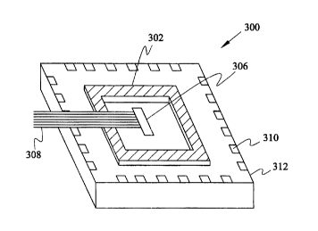
With reference to Figures 3 through 6, in an exemplary embodiment, a packaged
component suitably comprises: a chip earner 312; a component 306; at least one
connection 308; and a lid 400. With additional reference to Figures 23 to 33,
the chip
earner 312 may comprise any suitable component receptacle such as quad package
2300
with side flat leads or J-leads, pin grid array package 2500, column grid
array package
2800, ball grid array package 3100, and the like. In a preferred embodiment,
the chip
carrier 312 is preferably a surface mount chip carrier with a plurality of
terminals 310 to
facilitate connections to other components, circuits, and the like. Chip
carrier 312 is
suitably configured with a metal rim 302, suitably formed from a high
temperature alloy
with a low thermal expansiion coefficient, such as the commercially available
product
KOVAR. Additionally, metal rim 302 is suitably coated with a solderable and
corrosion
resistant material, such as zinc, tin, lead, copper, and the like.
With continued reference to Figures 3 through 6, the component 306 suitably
comprises an opto-electronic component, such as a laser diode, an optic chip,
and the
like, and is suitably mounted on chip carrier 312. The connection 308 suitably
comprises a plurality of optical fibers 308 connected to the component 306.
When
multiple optical fibers 308 are used, the optical fibers 308 may be mounted on
silicon v-
grooves to suitably support and separate the fibers 308. In a preferred
embodiment,
multiple optical fibers 308 are suitably configured as flat ribbon fiber. As
discussed in
greater detail below, optical fibers 308 are coated with suitable metals (such
as zinc, tin,
CA 02346361 2001-04-06
WO 00/21130 PCT/US99/22606
-6
lead, copper, nickel, and the like) to facilitate solder adhesion and
corrosion resistance.
In a preferred embodiment, optical fibers 308 are coated with gold and nickel
(available
from Spectran of Avon, Connecticut). Although one set of optical fibers 308 is
depicted
in Figures 3 through 6, any number of single or multiple optical fibers, or
any
combination thereof, may tie connected to opto-electronic component 306. For
example, with reference to Figures 21 and 22, two or more sides of opto-
electronic
component 306 may be corurected to any number of optical fibers.
Alternatively, opto-
electronic component 306 may be configured in an elliptical configuration with
optical
fibers connected radially. li urther, connection 308 may comprise any
appropriate
l0 connection, such as a wire ~or a waveguide.
With particular reference to Figures 5 and 6, in accordance with various
aspects
of the present invention, the lid 400 is suitably disposed on chip carrier
312. Lid 400 is
preferably configured as a rigid structure and may be formed of any
appropriate strong
and rigid material, and is preferably solderable and corrosion resistant. In
an exemplary
embodiment, package lid 400 is formed from a high temperature alloy with low
thermal
expansion coefficient material, such as the commercially available product
KOVAR.
For lid materials that are not generally solderable or corrosion resistant,
lid 400 is
suitably coated, for example electroplated in solderable and corrosion
resistant material
such as zinc, tin, lead, copper, and the like. In a particular preferred
embodiment, lid
400 is electroplated in 50 to 150 microinches of electroless nickel in
accordance with
military standard MIL-C-26074 Class 1, followed by 50 to 150 microinches of
gold in
accordance with military standard MIL-G-45204, type III, grade A.
With reference again to Figure 5, lid 400 may be formed using any convenient
method such as machining, stamping, and the like. For example, if only a small
number
of lids are required, machining may be a more cost effective method than
stamping. In
contrast, far large numbers. of package lids, stamping may be more cost
effective.
Alternatively, in some applications, these two methods may be combined. For
example,
a large number of standard lids may be formed by stamping and customized for
particular applications by machining. Additionally, with reference to Figure
12, when
stamping is used, package lid 1200 may be configured with a raised cavity 1202
rather
than a recessed cavity (Figure 9) for ease of manufacture.
CA 02346361 2001-04-06
WO 00121130 PC'T/US99/22606
Additionally, lid 400 may be configured in any appropriate shape and
dimensions for particular applications. For example, lid 400 may be
rectangular to
substantially conform with rectangular rim 302. Similarly, package lid 400 may
be
relatively tall or short to accommodate the height of opto-electronic
component 306.
With reference to Figures 8 through 10, in an exemplary embodiment of the
present
invention, lid 400 is preferably substantially square in shape with lengths
802 and 804
of about 0.522 inches and thickness 1000 of about 0.046 inches.
With reference to Figures 9 and 1 l, a cavity 900 is suitably formed in the
underside of lid 400 to provide clearance for opto-electronic component 306
and
plurality of optical fibers 308 (Figure 3). A lip 410 is suitably configured
to
substantially conform with metal rim 304 (Figure 3). In an exemplary
embodiment of
the present invention, the thickness 1002 of cavity 900 is about 0.23 inches,
and the
thickness 902 of lip 910 is about 0.061 inches.
A component package according to various aspects of the present invention
includes a connection slot a.nd a sealant slot. For example, as particularly
depicted in
Figure 5, at least one connection slot 404 is suitably configured in lid 400
as access for
optical fibers 308. More particularly, with reference to Figures 9 and 11,
connection
slot 404 is suitably formed through lip 910 and into cavity 900. Additionally,
sealant
slot 402 and is formed proximate, such as above, and opens into connection
slot 404.
As described in greater detail below, when a sealant, such as solderable
material,
disposed in sealant slot 402 melts, it flows through sealant slot 402 to
hermetically seal
optical fibers 308 within connection slot 404. A compliant and flexible sleeve
500 is
suitably secured to optical fibers 308 and attached to lid 400 using adhesive
material,
such as epoxy, to provide tension relief.
Although one connf;ction slot 404 and one sealant slot 406 are depicted, any
number of connection slots and sealant slots may be disposed at any number of
locations around the perimeter of lid 400. For example, with additional
reference to
Figure 22, four connection slots 404 and four sealant slots 406 are suitably
configured in
lid 400 as access for four sf;ts of optical fibers 308. Additionally, the
dimensions of
3o sealant slot 406 are suitably selected to facilitate use of a sufficient
amount of sealant to
hermetically seal plurality of optical fibers 308 in connection slot 404. In
an exemplary
embodiment of the present invention, length 806 of sealant slot 402 and length
904 of
CA 02346361 2001-04-06
WO 00/21130 PCT/US99/22606
_g_
connection slot 404 are about 0.230 inches. Width 810 of sealant slot 402 is
about
0.023 inches. Thickness 1006 of connection slot 404 is about 0.008 inches.
In accordance with ;gin alternative embodiment of the present invention,
connection slots may be formed in the main package rather than the lid. More
particularly, with reference to Figures 13 and 14, in main package 1400,
connection slot
1406 is suitably formed in metal rim 1404 of chip carrier 1402. Lid 1300
includes
sealant slot 1302 for receiving sealant to seal optical fibers fed through
connection slot
1406 and into cavity 1304. This configuration may be advantageous in
applications
where modification of chip can-ier 1402 may be simpler and more cost effective
than
to modifying lid 1300.
With reference to Figures 3 and 5, a preform of corrosion resistant solder
material (such as gold-tin, lead-tin, indium based solder, and the like) is
suitably
attached to lid 400 or metal ring 302. Package lid 400 is suitably sealed to
metal ring
302, for example using any convenient welding method, such as projection and
seam
electrical welding, electron and laser beam welding, and the like, to reflow
the solder
material disposed between lid 400 and metal ring 302. In addition, localized
heat {such
as hot air) is suitably applied to connection slot 404 and sealant slot 402 to
reflow
sealant, such as corrosion resistant salder material, disposed in sealant slot
402. More
particularly, the solder material flows down into connection slot 404 and
adheres to the
2o metallized coating of optical fibers 308 to form a hermetic seal. In this
manner, heat
damage to opto-electronic component 306 (Figure 3) may be reduced.
Alternatively, if
opto-electronic component 306 is resistant to heat damage, the entire assembly
can be
placed into an oven for solder reflow.
In accordance with various aspects of the present invention, a hermetically
sealed opto-electronic package may be configured with various interface
schemes. For
example, with reference to Figures 15 and 16, a pigtail interface scheme 1500
includes
hermetically sealed opto-electronic package 1502 which is connected to a
ferrule 1506
by an optical fiber pigtail 1504. Ferrule 1506 is preferably standardized to
facilitate
flexible connections to other components, circuits, and the like.
3o With reference to Figures 17 and 18, a module-on-board interface scheme
1700
includes an opto-electronic package 1702 and a connector receptor 1706
suitably
disposed on an integrated circuit board 1708. Optical fibers 1704 connect opto-
CA 02346361 2001-04-06
WO 00/21130 PCT/US99/22606
-9
electronic package 1702 and connector receptor 1706. Connector receptor 1706
is
preferably standardized to facilitate flexible connections to other
components, circuits,
and the like.
With reference to Figures 19 and 20, a connectorized-module interface scheme
1900 includes an opto-electronic package 1902 and a connector receptor 1906
suitably
disposed within a connectorized housing 2000. Additionally, a coupling recess
1908 is
suitably formed in connectorized housing 2000 to engage with a coupling member
(not
shown). Connector receptor 1906 and coupling recess 1908 are preferably
standardized
to facilitate flexible connections to other components, circuits, and the
like.
to Although the present invention has been described in conjunction with
particular
embodiments illustrated in the appended drawing figures, various modifications
may be
made without departing from the spirit and scope of the invention as set forth
in the
appended claims. For exarr~ple, if hermetic sealing is not required, the
present invention
may be used in conjunction with nonhermetic packaging by using glue (such as
epoxy)
seal rather than soldering.