Note: Descriptions are shown in the official language in which they were submitted.
CA 02346654 2001-04-05
W~ C0/22477 1 PCT/SE99/01807
Electro-absorption modulator and method for manufacturing of such a modulator
TECHNICAL FIELD OF THE INVENTION
The present invention relates partly to an electro-absorption
modulator, particularly with improved performance, partly to
different methods for manufacturing of such an electro-
absorption modulator.
DESCRIPTION OF RELATED ART
Electro-absorption modulators (EAM), particularly of the kind
that includes a waveguide, and often monolithically integrated
together with so-called DFB lasers (Distributed Feedback
Lasers), is a very important component class for fiber optic
transmission at high bit rates (typically 2,5 Gb/s and 10 Gb/s;
in the future most likely 40 Gb/s) in combination with long-
haul transmission.
The reason for this is that such EP.M components have more ideal
characteristics than, for instance, directly modulated lasers
(specifically, they have less dynamic wavelength deviations,
so-called chirp, during modulation). Furthermore, they are
considerably simple to manufacture and require only a low
driving voltage (compared to other classes cf external optical
modulators, such as, e.g., Mach-Zender modulators manufactured
in lithium neobate). Not at least, the EAM component is very
useful for applications including wavelength division
multiplexing (WDM).
A conventional EAM component consists of a waveguide, with a
waveguide core whose refractive index is higher than that of
the surrounding, see for instance EP 0,809,129, EP 0,726,983,
GB 2,281,785, and references therein. For components operating
with launched light of a wavelength of 1.3 0. 1.55 Eun, the core
consists typically of a semiconductor material, such as InGaAsP
or alternating layers of InGaAsP and InP. The core is undoped
or only slightly doped. Above and below th' core, there are
CA 02346654 2001-04-05
WQ OOI22477 2 PCT/SE99/01807
typically a p-doped InP layer and an n-doped InP layer,
respectively, so that the complete structure composes a p-i-n
diode.
The attenuation through the modulator depends on the difference
in energy between the photons of the launched light and the
band gap of the core. The band gap is affected, inter alia, by
the electrical field applied. Thus, the p-i-n diode is arranged
so that, when it is reverse biased, a large portion of the
launched light is absorbed, whereby a photo current arises.
Typically, extinction ratios of 10 - 30 dB may be achieved.
A problem in this respect is that the band gap is also strongly
temperature dependent. The photo current that arises, causes
ohmic heating, and thus a temperature rise, whereby the
attenuation is affected. The absorptionen, which in a first
approximation is proportional to the luminous power, is highest
in the beginning of the modulator, i.e., where the light is
launched into the modulator, whereby also the photo current is
highest there. Thus, the strongest affection of the attenuation
is achieved there.
SU~RY OF THE INVENTION
To conceive how this temperature dependence may create problems
in a digital transmission system, let us consider the following
example. Suppose that one wants to send one or several
consecutive "ones", preceded by a long sequence o' "zeros" .
These "zeros" correspond to a reverse biased diode. According
to the discussion above, this results in a large temperature
increase, particularly then in the beginning of the modulator.
When the voltage then is changed to a lower value,
corresponding to a transmitted "one" , an optical pulse out of
the diode is achieved. Instead of a sharp flank, reflecting the
difference in externally applied voltage, a slow building-up
process is achieved; only after a certain period of time the
component has approached a constant value of the optical power
CA 02346654 2001-04-05
WO 00!22477 3 PCTlSE99/01807
level for the "one". This clearly restricts the bandwidth of the
transmission medium.
It is an object of the present invention to provide an electro-
absorption modulator with improved performance.
It is a further object of the invention to provide an electro-
absorption modulator in lack of problems that arise because of
the strong temperature dependence of the band gap in the core
of the modulator.
It is in this respect a particular object of the invention to
provide an electro-absorption modulator that provides an
optical pulse with short rise time when the voltage over the
modulator is reduced.
It is yet another object of the invention to provide a method in
manufacturing of said electro-absorption modulator.
Further objects of the present invention will be apparent from
the specification below.
According to a first aspect of the present invention, an
electro-absorption modulator (EAM), of the kind that includes a
waveguide, for modulation of light, is provided, comprising a
waveguide core, a waveguide cladding and an electrode, the
modulator being arranged to modulate light launched into the
modulator as a response to a voltage being applied to the
electrode. The modulator is characterized in that the width
and/or thickness of the waveguide core are/is varying along the
length of the modulator in such a way that the width is smaller
in the portion of the modulator where the light is intended to
be input, for the purpose of reducing the absorption o~ the
modulator there.
This variation is particularly arranged so that a mainly
uniform photo current distribution, and thus temperature
distribution, is achieved along the length of the modulator,
CA 02346654 2001-04-05
WO 80/22477 4 PCT/SE99/01807
for the purpose of reducing the thermally dependent, optical
rise time of the modulator.
The electro-absorption modulator is preferably arranged to be
used for intensity modulation of digital signals for fiber
optic transmission. It may be monolithically integrated with a
DFB laser (Distributed Feedback Laser) on a semiconductor
substrate and manufactured using any of the material systems
InP/InGaAsP, InP/InGaAIAs or GalnAs/AlGaAs.
The waveguide core may be of bulk or quantum well structure and
the waveguide may be formed as a buried waveguide or as a, so-
called, ridge waveguide.
According to a second aspect of the present invention there is
provided a method in manufacturing of an electro-absorption
modulator (EAM) according to the first aspect.
To manufacture a waveguide core with a varying width along the
length of the modulator, so-called tapered photolithography
masks, or selective etching may be used. If a waveguide core
with quantum well structure is manufactured, inactive so-called
SCH (Separate Confinement Heterostructure) layers in the
quantum well structure may be etched selectively.
To manufacture a waveguide core with a varying thickness along
the length of the modulator, SAE (Selective Area Epitaxy).or
partially making the waveguide core thinner, through masking
and etching, may be used.
An advantage of the present invention is that intensity
modulation can be performed faster, which gives a higher
transmission capacity.
BRIEF DESCRIPTION OF THE DRAWINGS
The invention is described in detail hereinbelow with reference
to the accompanying Figures, which are given by way of
CA 02346654 2001-04-05 I
WO 00,122477 PCT/SE99/01807
illustration only, and thus are not limitative of the present
invention.
Fig. 1 illustrates, in cross section, an electro-absorption
modulator according. to prior art.
Fig.. 2 illustrates .an example of an optical output signal from
the modulator of Fig. 1 as a response to an electrical input
signal consisting of three "zeros" followed by five "ones" .
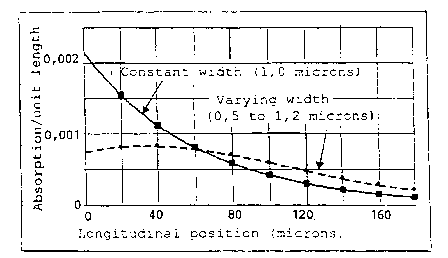
Fig. 3 illustrates estimated relative absorption per length
unit as a function of longitudinal position coordinate for a
known modulator with a constant waveguide width, and for a
modulator with a varying width ("tapered" structure) according
to a preferred embodiment of the present invention.
Fig. 4 illustrates the main steps in a so-called BH (Burried
Heterostructure) process in manufacturing of an electro-
absorption modulator with varying waveguide width according to
a preferred embodiment of the present invention.
Fig. 5 illustrates the main steps in a process using selective
etching in manufacturing of an electro-absorption modulator
with varying waveguide width according to an alternative,
preferred embodiment of the present invention.
DETAINED DESCRIPTION OF EMBODIMENTS
In the following description, for purposes of explanation and
not .limitation, specific details are set fourth, such as
particular applications, techniques, methods etc. in order to
provide a thorough understanding of the present invention.
However, it will be apparent to one skilled in the art ti~at the
present invention may be practiced in other versions that
depart from these specific details. In other instances,
detailed descriptions of well-known methods, protocols, devices
or-circuits are omitted so as not to obscure the description of
the present invention with unnecessary details.
CA 02346654 2001-04-05
WO OO/Z2477 PCT/SE99/01807
6
Referring to Fig. 1, a previously known EAM component 100 of a
semiconductor material, normally InP/InGaAsP, a waveguide with
a waveguide core 101 of bulk or quantum well structure, called
i layer, whose refractive index is higher than that of the
surrounding. For launched light at a wavelength of 1.3 or 1.55
Ecm, the core shall typically consist of a semiconductor
material such as InGaAsP for bulk structure, or alternating
layers of InGaAsP and possibly InP for quantum well structure.
The core is typically slightly doped or not doped at all. Above
the core there is a p-doped InP layer 103 and below the core
there is an n-doped InP layer 105. Thus, this structure
constitutes a p-i-n diode. Alternatively, the upper layer is n-
doped and the lower layer p-doped.
On both sides of the wavelength core there is InP, which may be
doped or undoped (not shown in Fig. 1); most usually this
material consist of semi-isolating InP. Above the upper
cladding layer 103 there is a contact layer 107, on which an
electrode 109 is formed. Layer 111 of semi-isolating InP may
also be formed between the core 101 and the upper cladding
layer 103 in front of and behind the electrode 109, e.g., for
isolating purposes. The width of the waveguide core is
typically about 1 ~m (for single mode waveguides).
Laser light 113 is launched into the modulator 100 from left-
hand side in Fig. 1 and the modulated light 115 is output from
the modulator to the right in said Fig. The attenuation through
the modulator depends on the voltage being applied on the
electrode 109. If the p-i-n diode is reverse biased a strong
electrical field over the i layer 101 arises. This will then
cause absorption of a large portion of the injected laser J_ight
113. This is well known and is called electro-absorption. If
the core consists of bulk material the phenomenon is named
Franz-Keldysh effect and if the core consists of quantum wells
the phenomenon is named Stark effect.
CA 02346654 2001-04-05
WO OOI22477 7 PCT/SE99/01807
With a modulator length of 100 - 300 dun, and a thickness of the
i layer between 0.1 and 0.4 ~m (which are typical values),
extinction ratios of 10 - 30 dB may be achieved provided that a
voltage of the order of 2 V is applied on the electrode. With
extinction is meant the relative difference between the optical
output power from the modulator when a "one" is being
transmitted (low or no voltage of the modulator electrode) and
the optical output power when a "zero" is being transmitted
(high negative voltage, one or several volts, on the
electrode).
The value of the extinction depends on the difference in energy
between the photons of the input light and band gap of the
material in the i layer. The smaller this difference is, the
larger change in absorption per applied unit voltage is
achieved. It depends on that electro-absorption is a so-called
resonant physical phenomenon.
It may be understood in the following way. By applying an
electrical field over the i region the bard gap of the material
is reduced, which gives rise to an increased absorption, given
the light energy being lower than the band gap energy. If for
instance light of a wavelength of 1.55 Etm (which corresponds to
a photon energy of 0.8 eV) is coupled into the modulator, an i
layer in the modulator with a band gap in the interval of 0.82
- 0.88 eV is typically chosen.
The. light that is absorbed generates a photo current. Each
absorbed photon creates an hole/electron pair, which is
separated in the applied electrical field. Some holes and
electrons do not have time to recombine before they reach the
contacts, but in a well designed component a high external
quantum efficiency (>90%) is achieved if the component is
regarded as a photo diode.
In the beginning of the modulator the optical power is highest.
It means that the absorption is strongest there, when a reverse
CA 02346654 2001-04-05
WO QOIZ2477 8 PCT/SE99/01807
bias is applied on the electrode. The optical power in the
waveguide is then decreasing, in a first approximation
exponentially, to be very low in the final portion of the
modulator. This indicates that the photo current density
generated is largest in the beginning of the modulator (to the
left in Fig. 1).
It will be appreciated that this may cause serious problems,
particularly in the case one wishes to obtain high extinction
ratios and at the same time inject a great amount of light into
the EAM waveguide. The reason is local heating. With a reverse
bias of several volts, and a photo current of 10 - 25 mA
(corresponding to optical input powers of 8 - 20 mW for 1.55 Eun
wavelength; such optical powers are easily achieved when the
EAM component is monolithically integrated with a DFB laser
(Distributed Feedback Laser) or. the same semiconductor
substrate), a strong, local ohmic heating of the waveguide is
obtained. The heat power per area unit generated is given by
the local photo current density multiplicated by the voltage
drop over the i layer. The heating gives rise to a locally
increased temperature. With a thermal resistance in the order
of 1000 K/W in a 25 ~.un long waveguide segment, local
temperature increases of tens oz Kelvins may easily be
obtained. The temperature increase will though be nonuniformly
distributed along the length of the modulator in a similar
manner (though not identical) as the photo current density.
This may introduce serious problems in a digital transmission
system, which is seen by study the following example. One wants
to send one or several consecutive "ones" , preceded by a long
sequence of "zeros". These "zeros" correspond .to a large
reverse biasing voltage being applied over the i layer (which
gives strong absorption). According to the reasoning above,
this results in a large temperature increase, particularly in
the beginning of the modulator (to the left in Fig. 1).
CA 02346654 2001-04-05
WO 00/22477
PCT/SE99101807
' ' 9
When the voltage then is changed to a lower value,
corresponding to a transmitted "one", an optical output pulse
from the EAM component similar to the one in Fig. 2 is
obtained.
Fig. 2 shows an example of electrical input signal (squares)
and optical output signal (rhombs) for a modulator as a
function of time. The input signal consists here of three
"zeros" followed by five "ones". Strong heating occurs in the
beginning of the modulator caused by a strong absorption per
length unit at negative bias (-2 V).
Instead of a sharp flank, reflecting the difference in
externally applied voltage, a slow building-up process is
obtained. Only after a certain period of time the component has
approached a constant value of the optical power of the "one".
Note that for NRZ modulation with a transmission capacity of 10
Gb/s, a time scale period in the Figure corresponds to 0.2
nanoseconds.
The reason for this behavior is that the absorption
coefficient, except of depending on the electrical field
strength, also depends strongly on the temperature, which in
turn depends on that the band gap of the semiconductor material
is temperature dependent. After a long sequence of "zeros" the
absorption remains thus high even when the applied reverse bias
is reduced, since the temperature is higher and the band gap in
the i layer is smaller. The time constant for the settling to
the -steady state in Fig. 2 is dependent on the precise
arrangement of the waveguide and surrounding layers. One can
easily show that it is quite possible to achieve a time
constant of less than 1 ns, since the absorption is occurring
within a very small region. None the less, this optical rise
time is bandwidth limiting and it is desirable to decrease it,
particularly to a considerable extent.
CA 02346654 2001-04-05
WO Op/22477 1~ PCT/SE99/01807
By realizing the problem as discussed above and by vary the
optical confinement factor in the actively absorbing layer in
such a way that a more uniform photo current distribution along
the length of the modulator, an electro-absorption modulator
according to the principles of the present invention is
achieved.
Hereby, locally, largely increased temperatures are avoided,
whereby an electro-absorption modulator with a shorter optical
rise time is obtained.
Instead of having a constant width and thickness of the
waveguide core, the width and/or the thickness are/is varied
along the modulator. Closest the point where light is injected
(to the left in Fig. 1) the waveguide core is preferably made
narrow/thin whereas it preferably is made wider/thicker closest
to the point where light is emitted from the waveguide core.
With this arrangement the optical confinement factor is varied,
and thus the absorption. In the beginning of the modulator the
optical confinement factor is small, whereby also the
absorption is small. This means that the heat release is
smaller there than if the modulator had been wider and/or
thicker. Further on, when the optical power has decreased due
to the absorption, the width and/or the thickness of the
waveguide core of the modulator are/is increased, whereby the
absorption is increased.
In this way a more uniform photo current distribution along the
modulator is achieved, and one avoids largely increased
temperatures locally within a small region closest to the
optical injection point.
The absorptionen in an EAM modulator depends on the optical
confinement factor and the field strength applied. I~ will have
the following consequences.
CA 02346654 2001-04-05
WQ 00/22477 11 PCT/SE99/01807
If only the width of the waveguide core is varied, the applied
voltage on the modulator electrode will give a relatively
constant electrical field strength over the i layer of the
modulator independent of its length. A certain dependence
between field strength and width may, however, exist due to an
increased electrical resistance and thus voltage drop if the
waveguide is made narrow. In such circumstances, the desired
effect is augmented.
To achieve a perfectly uniform absorption (and thus photo
current distribution) along the modulator, the width of the
waveguide core shall thus be increased so.that the increase in
confinement factor completely compensates the decrease in
optical power, due to absorption, in such a way that the
optical power in the core becomes constant along said core.
If only the thickness of the waveguide core is varied, also the
field strength over the i layer will vary. A thin waveguide
segment achieves high field strength (which gives strong
absorption) and low optical confinement factor (which gives
weak absorption). In other words, there are two counteracting
effects present if the optical confinement factor is varied
through varied waveguide thickness.
The absorption as a function of the core thickness has a
maximum for some thickness (the limits of infinitely small
thickness and infinitely large thickness, respectively gives
zero absorption).
To achieve a more uniform absorption (and thus photo current
distribution) along the modulator, the thickness of the
waveguide shall thus be increased towards the modulator output
if the thickness is smaller than the thickness corresponding to
maximum absorption, which in practice most often would be the
case.
CA 02346654 2001-04-05
WO 00/22477 PCT/SE99/01807
12
An optimal variation of width and/or thickness may preferably
be estimated numerically.
Fig. 3 shows estimated relative absorption per length unit as a
function of longitudinal coordinate for a conventional
structure with constant waveguide width, and for a structure
with varying width, so-called tapered structure, according to
the present invention. Light is injected at x = 0 Vim.
The waveguide consists of a quantum well structure (ten undoped
quantum wells of InGaAsP surrounded by undoped InGaAsP-barriers
with larger band gap than the wells). The modulator is in this
example 180 ~m long. The component has been reverse biased to a
level where the material absorption is 500 cm 1. The waveguide
core of the conventional structure has a constant width of 1.0
N.m, whereas the waveguide core of the inventive tapered (i.e.
with a varying width along the waveguide) structure has a width
that varies linearly from 0.5 to 1.2 Vim. The thickness of the
waveguide is in this example kept constant.
As can be seen in Fig. 3, a much more uniform, i.e., mainly
uniform, distribution of the absorption along the modulator is
achieved with the tapered structure. It leads to a more uniform
temperature distribution, and prevents intense local heating in
the beginning of the modulator.
Preferably, the electro-absorption modulator, according to the
present invention, is intended for intensity modulation of
digital signals for fiber optic transmission. It may be alone
or monolithically integrated with a laser source.
Besides, if the EAM component is to be adapted for higi: bit
rates, it has to be manufactured with low capacitance, i.e.,
with short length, since the capacitance together with the
equivalent resistance of the electrical driving circuit affect
the rise and fall times of the modulated light.
CA 02346654 2001-04-05
WO 00/22477 13 PCT/SE99/01807
To manufacture an inventive modulator with varying
width/thickness may be done in several ways. In the following,
five examples of approaches will be discussed briefly, with
reference to Figs. 4 and 5.
The first method produces a waveguide core with varying width
by using a tapered photolithography mask. The waveguide core is
defined by conventional photolithography, for example contact
lithography, projection lithography, E-beam lithography or
similar, and subsequent etching. The photolithography mask to
be used, shall, according to the present invention, be tapered,
whereby'also the waveguide core will be tapered.
Main steps in the process are visualized in Fig. 4, which
Figure illustrates a so-called BH process (Burried
Heterostructure), but the invention is applicable also to
other, modified classes of laser/modulator processes, e.g., for
manufacturing of ridge lasers. Fig. 4. shows I. waveguide core
mask seen from above, II. cross sections along lines A-A and B-
B in I. after masking but before etching, III. same cross
sections after etching, and IV, same cross sections after
completed process. In the Figure the reference numeral 41
denotes waveguide core, 42 denotes n-doped InP, 43 denotes p-
doped InP, 44 denotes semi-isolating InP, 45 denotes electrode,
and 46 denotes mask.
The second method produces a waveguide core with varying width
by selective etching. By using a selective etch, preferably an
wet etch, which etches waveguide core material, but not
surrounding material, in combination with masking of waveguide
segments which are not to be etched, a waveguide with different
width in different segments is achieved. This gives discrete
steps in waveguide width, but by repeating the etching step
several times with masks of different lengths, a more
continuous variation of the waveguide width is achieved.
CA 02346654 2001-04-05
WO00/22477 14 PCT/SE99/01807
Fig. 5. shows different main steps according to this
alternative method for achieving waveguides with varying width.
Thus, the Figure shows I. waveguide mask as seen from above,
II. cross sections along lines A-A and B-B in I. after masking
but before etching, III. same cross sections after etching, IV.
same cross sections after selective etching, and V, same cross
sections after completed process. In the Figure the reference
numeral 51 denotes waveguide core, 52 denotes n-doped InP, 53
denotes p-doped InP, 54 denotes semi-isolating InP, 55 denotes
electrode, 56 denotes waveguide mask and 57 denotes mask for
selective etching.
The third method produces a waveguide core with varying width
by selective etching away of inactive SCH (Separate Confinement
Heterostrukture) layers, i.e., layers in the waveguide which
have as a task to affect the optical confinement factor, which
are, inter alia, used in quantum well structures.
The fourth method produces a waveguide core with a varying,
tapered, thickness by using SAG (Selective Area Epitaxy). A
mask of, e.g., silicon oxide or silicon nitride is placed on
the structure before epitaxy of the waveguide core. The rate of
growth, and thus the thickness of the waveguide core layer, the
i layer, depends on the distance to the mask. With a suitable
design of the mask, a layer with tapered thickness is achieved.
The fifth method produces a waveguide core with tapered
thickness by partially making the core layer thinner. The
varying thickness is achieved by making the core layer thinner
(using masking and etching) within areas where the layer should
be thin. This gives discrete steps in core layer thickness, but
through repeating the step several times with different masks, -
one may achieve a more continuous variation of the waveguide
core thickness.
A combination of two or more of the above described methods is
obviously also applicable.
CA 02346654 2001-04-05
WO 00122477 PCT/SE99/01807
The invention is apparently not limited to the embodiments as
described above and illustrated in the Figures, but may be
modified within the scope of the appended claims. Particularly,
the invention is obviously not limited as regards material,
dimensions or manufacturing method of the electro-absorption
modulator.