Note: Descriptions are shown in the official language in which they were submitted.
CA 02346714 2001-04-06
TITLE OF THE INVENTI()N
RECEIVER FOR OFDM PACKET COMMUNICATION SYSTEM
FIELD OF THE INVENTI()N
The present invention relates to a packet
communication receiver used in OFDM (Orthogonal
Frequency Division Multiplexing) digital wireless
communication systemõ In particular, it relates to
an OFDM receiver for demodulating OFDM signals
accurately with little process delay and high
transmission efficiericy, even when there is a
sampling clock frequency error and/or a carrier
frequency error between a transmitter and a
receiver, and/or received signals are affected by
phase noise and/or ttiermal noise.
BACKGROUND OF THE INVENTION
An OFDM system is a kind of multicarrier
transmission system which divides an original high
rate signal stream irito a plurality of low rate
parallel signal streams and transmits them
simultaneously. In ari OFDM system, each subcarrier
is closely located orthogonally with one another on
the frequency axis. In general, when high rate
signals are transmitt:ed through wireless channel,
signal quality will be degraded because of inter-
symbol interference ciue to multi-path propagation
caused by reflection and/or diffraction. However,
in multicarrier systems such as OFDM systems,
inter-symbol interfei-ence due to multi-path
1
CA 02346714 2001-04-06
propagation is mitigated, because transmission rate
of each subcarrier is decreased by the parallel
transmission even in high rate transmission.
Moreover, OFDM systems have an advantage that
each subcarrier can be easily multiplexed at a
baseband process part of a transmitter by using
inverse fast Fourier transform (IFFT), and each
subcarrier can be easily de-multiplexed at a
baseband process part of a receiver by using fast
Fourier transform (FFT). Therefore, both a
transmitter and a receiver can be simplified in
structure. Further, by utilizing the nature of
Fourier transform, a transmitter may transmit each
OFDM symbol having a guard interval which is
obtained by cyclica:L extending an inverse fast
Fourier transform output, and a receiver takes only
signals which have less inter-symbol interference
in OFDM signal strearn by using FFT window, so that
inter-symbol interference is further decreased.
Furthermore, because of the presence of a guard
interval, a receiver can demodulate signals with no
interference originated in adjacent symbols, even
when symbol timing, i.e. FFT window timing, has a
small timing error wiLthin said guard interval due
to noise component and suchlike. Thus, no accurate
timing synchronization, which is essential in
single-carrier transmission systems, is required in
OFDM systems. Accordingly, OFDM systems are
suitable for high rate radio transmission.
A prior OFDM packet communication receiver is
2
CA 02346714 2001-04-06
described in accordance with Fig.43. It is assumed
that a packet format shown in Fig.44 is used to
transmit OFDM signals.
In Fig.43, OFDM signals received by an antenna
1 are fed to a receiving circuit 2, which carries
out receiving process including frequency
conversion, filtering, orthogonal detection and
analog-to-digital (A/D) conversion to input OFDM
signals, and outputs baseband signals in complex
form. Clock frequency error information signals
provided by a clock frequency error detector 8 are
fed to the receiving circuit 2. The details of a
clock frequency error will be described later. The
receiving circuit 2 carries out said receiving
process and compensates the sampling clock
frequency by controlling an analog oscillator which
is used for A/D conversion and others by using said
clock frequency error information.
Output complex baseband signals of the
receiving circuit 2 are fed to a synchronization
circuit 3, which detects both carrier frequency
error and OFDM symbol timing by using preamble
signals for synchronization located in the header
part of a packet, anci outputs complex baseband
signals after the carrier frequency error
compensation process by using said detected carrier
frequency error information. Moreover, the
synchronization circuit 3 also outputs said
detected OFDM symbol timing information. The OFDM
symbol timing information is used in a succeeding
3
CA 02346714 2001-04-06
guard interval removing circuit 4 which removes
signals corresponding to guard intervals from the
complex baseband signals, and extracts signals
which are fed to a Fourier transform circuit 5.
Output signals of the synchronization circuit
3, which are the signals with carrier frequency
error compensated and the OFDM symbol timing
information signal, are fed to the guard interval
removing circuit 4. The guard interval removing
circuit 4 removes the signals corresponding to the
guard interval from each OFDM symbol by applying
the FFT window having time width equal to the
difference of OFDM symbol duration and guard
interval length so that the signals which should be
fed to the Fourier transform circuit 5 are
extracted.
The output signals of the guard interval
removing circuit 4 a.re fed to the Fourier transform
circuit 5, which cariries out fast Fourier transform
to the input signals which are free from the guard
interval to provide frequency components of each
subcarrier, and outputs subcarrier signals each
separated on baseband region. The Fourier transform
circuit 5 carries out fast Fourier transform for
each OFDM symbol, and outputs subcarrier signals of
each OFDM symbol.
Subcarrier signals, which are the output
signals of the Fourier transform circuit 5, are fed
to a coherent detection circuit 7, a channel
estimator 6 and a clock frequency error detector 8.
4
CA 02346714 2001-04-06
The clock frequency error detector 8 detects phase
rotation of each subcarrier caused by sampling
clock frequency error used in the receiving circuit
2, calculates sampling clock frequency error
between a transmitter and a receiver based upon the
detected phase rotation of the subcarriers, and
outputs calculated clock frequency error
information.
For example, in the case where 16QAM
modulation scheme is used to modulate each
subcarrier, a signal after coherent detection is to
locate one of 16 reference signals Sl through S16
as shown in Fig. 45. However, when there exists a
sampling clock frequency error between a
transmitter and a receiver, the signals which are
coherent detected are subject to said phase
rotation, and output signals from the coherent
detection circuit 7 (e.g., R1 or R2 in Fig.45) do
not coincide with one of the reference signals S1
through S16.
Therefore, a clock frequency error detector 8
detects phase rotation of each subcarrier in each
OFDM symbol. For instance, when an output signal of
the coherent detection circuit 7 is R1 in Fig.45,
the clock frequency error detector 8 finds the
reference signal S3 which is the closest to the
input signal R1 among the reference signals S1
through S16, and detects the phase difference 0 1
between the reference signal S3 and the input
signal Ri. Further, when an output signal of the
CA 02346714 2001-04-06
coherent detection circuit 7 is R2 in Fig.45, the
clock frequency error detector 8 finds the
reference signal S6 which is the closest to the
input signal R2 among the reference signals S1
through S16, and detects the phase differenceo 2
between the reference signal S6 and the input
signal R2.
Now, the phase rotation of output subcarrier
signals of the Fourier transform circuit 5 in the
case where there is a sampling clock frequency
error between a transmitter and a receiver is
explained.
As mentioned above, the guard interval
removing circuit 4 removes signals corresponding to
a guard interval frorn each OFDM symbol by applying
an FFT window by using symbol timing information
obtained by preamble signals for synchronization
located in the header part of a packet. However,
when there exists a sampling clock frequency error
between a transmitter and a receiver, timing
difference between the symbol timing of each OFDM
symbol and the FFT wiLndow timing depends upon the
location of the OFDM symbol in the packet even in a
single packet. Therefore, the FFT window timing at
the OFDM symbol close to the head of a packet used
for channel estimation differs from FFT window
timing at other OFDM symbols.
When a sampling clock frequency in a
transmitter is fTCLx, a sampling clock frequency in
a receiver is fR,,x, and symbol timing difference of
6
CA 02346714 2001-04-06
an OFDM symbol which appears after t seconds from
the OFDM symbol used for channel estimation is A t,
the following equation is obtained.
t * f TCLK - ( t - L~ t) * f RCLK. ( 1)
When the ratio of sampling clock frequency
error between a transmitter and a receiver to their
reference sampling clock frequency is Ax, the
following equation is satisfied.
'~' x - ( fRCLK f TCLK ) /f CLK ( 2 )
where fcLK is a reference sampling clock frequency
for a transmitter and a receiver.
From said equations (1) and (2), said timing
difference At is expressed as follows.
0 t = ( f CLK / f RCLK ) * A x * t (3)
Considering that fCLK fRCLK/ that is fCLK/fRCLK-1, L, t
is approximated as follows.
At = Ox * t (4)
Thus, it should be appreciated that an FFT
window timing difference is proportional to elapsed
time (t) and ratio (,, x) of sampling clock
frequency error between a'transmitter and a
receiver to a refererice sampling clock frequency.
Above-mentioned FFT window timing difference
affects to phase rotation of each subcarrier signal
depending upon its subcarrier frequency because of
fundamental principles of Fourier transform.
Moreover, as an FFT window timing difference is
proportional to elapsed time (t), the phase
rotation is also proportional to elapsed time (t).
Assuming that A(t) is result of Fourier transform
7
CA 02346714 2001-04-06
of a(t), the result of Fourier transform of a(t+p
t) is A(t)*exp(j27tf,-'~ t). Therefore, when an FFT
window timing difference at the guard interval
removing circuit 4 is A t(-,Lx*t (equation (4)), a
subcarrier signal provided by the Fourier transform
circuit 5 has a phase rotation 0 e as follows.
A B = 27-C * f* t* A x (5)
where f is a frequency offset between a subcarrier
frequency and a centier frequency of a channel, t is
time of the current OFDM symbol elapsed from the
OFDM symbols for channel estimation, and Ax is
ratio of sampling clock frequency error between a
transmitter and a receiver to a reference sampling
clock frequency.
Thus, when there exists a sampling clock
frequency error between a transmitter and a
receiver, a subcarrier signal provided by the
Fourier transform circuit 5 has an undesirable
phase rotation which increases or decreases
proportional to time of the current OFDM symbol
elapsed from the OFDM symbols for channel
estimation, and frequency offset of the current
subcarrier from a channel center frequency.
The clock frequency error detector 8 detects
sampling clock frequency error between a
transmitter and a receiver, that is to say, phase
rotation originated iLn sampling clock frequency
error between a transmitter and a receiver, from
output signals of the Fourier transform circuit 5,
and calculates clock frequency error information
8
CA 02346714 2001-04-06
according to the equation (5).
The clock frequency error information is fed
to the receiving circuit 2. The receiving circuit
2 controls a frequency of an internal oscillator,
which corresponds to a sampling clock frequency for
AD conversion and others, according to said clock
frequency error information so that the sampling
clock frequency error between a transmitter and a
receiver is removed.
on the other hand, a channel estimator 6
estimates the condition of a transmission channel
which transmits the OFDM signals of a current
packet, by utilizing the received preamble signals
for channel estimation which are known, located at
the header part of the packet. Both amplitude and
phase of each subcarrier signal shall fluctuate
because of frequency selective fading caused by
multi-path propagation. In this case, it is
possible to estimate how amplitude and phase of
each subcarrier signal have fluctuated through
propagation path of the corresponding subcarrier by
comparing the received subcarrier signal with the
known reference sigrial.
output signals of the channel estimator 6,
i.e. the channel estimation results, are fed to a
coherent detection circuit 7, and a weighting
circuit 11.
The coherent detection circuit 7 carries out a
coherent detection pr.ocess to the input subcarrier
signals by compensati_ng each subcarrier signal for
9
CA 02346714 2001-04-06
amplitude fluctuation and phase fluctuation
originated in channeTw fluctuation and others by
using said channel estimation results. It should be
noted that propagation condition is almost constant
during one packet transmission, because a packet
length is sufficiently short in high rate packet
communication system:, which use OFDM technique and
suchlike. Therefore, the coherent detection process
can be performed everi to the succeeding data
symbols by using the channel estimation results,
which are estimated by using the preamble signals
for channel estimation at the header part of a
packet. Output signa]_s of the coherent detection
circuit 7 are fed to a pilot signal phase rotation
detector 10 and a phase compensator 9.
The pilot signal phase rotation detector 10
extracts known pilot signa:Ls which are transmitted
through at least one specific subcarrier on each
OFDM symbol, and detects phase rotation of each
extracted pilot signal originated in residual
carrier frequency error and phase noise. The phase
noise is the noise wh.ich is added to phase
component of the received signal due to
imperfection of analog devices of both a
transmitting circuit in a transmitter and a
receiving circuit in a receiver. A residual carrier
frequency error is the frequency error which is
undesirably left with the output signals of the
synchronization circuit 3 due to imperfection of a
carrier frequency syrichronization process at the
CA 02346714 2001-04-06
synchronization circuit originated in thermal noise
added in the receiving circuit 2 and others.
Now, phase rotation of output signals of the
coherent detection circuit 7 in the case where
there exist residual carrier frequency error and/or
phase noise is explained briefly.
When there is a residual carrier frequency
error, a common frequency error is added to all the
subcarrier frequencies of output OFDM signals of
the synchronization circuit 3. Therefore, phase
rotation 00 of each subcarrier originated in a
residual carrier frequency error is expressed as
follows.
A ?/i = 27c' f * t (6)
where Of is a residual carrier frequency error,
and t is elapsed time from the channel estimation
at the header part of a packet.
As shown in the equation (6), the phase
rotation of each subcarrier originated in a
residual carrier frequency error is common to all
the subcarriers, and constant amount of phase
rotation increases for eacti OFDM symbol.
On the other hand, it can be assumed that
phase rotation added to each OFDM signal originated
in phase noise is cor.Lstant during one OFDM symbol,
because phase noise added to OFDM signals in the
receiving circuit 2 varies slowly compared to OFDM
symbol duration. Moreover, output signals of the
Fourier transform circuit 5 shall have the same
phase rotation as the phase rotation added to the
11
CA 02346714 2001-04-06
input signals in the case where common phase
rotation is added to input signals of the Fourier
transform circuit 5, because the Fourier transform
is a type of linear transform. Therefore, phase
rotation originated in phase noise is common to all
the subcarriers in one OFDM symbol, as is the case
of a residual carrier frequency error. Furthermore,
the change of phase noise among some adjacent OFDM
symbols is also small, because the phase noise
varies slowly compa.red to OFDM symbol duration as
above-mentioned.
By the way, it is fundamentally impossible to
compensate the phase rotation which varies for each
OFDM symbol, because the coherent detection circuit
7 carries out coherent detection process by the use
of the channel estimation result of each subcarrier
obtained by using the OFDM symbol for channel
estimation located at the header part of a packet.
Therefore, the coherent detection circuit 7 outputs
the signals which include phase rotation common to
all the subcarrier signals in each OFDM symbol,
originated in residual carrier frequency error and
phase noise.
The pilot signal phase rotation detector 10
detects phase rotation for each OFDM symbol
originated in residual carrier frequency error and
phase noise in pilot signals included in output
signals of the coherent detection circuit 7. The
pilot signal phase rotation extraction circuit 10
outputs phase rotation information of each pilot
12
CA 02346714 2001-04-06
signal. Output signa:ls of the pilot signal phase
rotation detector 10 are fed to a weighting circuit
11.
The weighting circuit 11 weights phase
rotation information which are provided by the
pilot signal phase rotation detector 10 according
to channel estimation result of each subcarrier
provided by the channel estimator 6. For instance,
when signal level of a subcarrier obtained by the
channel estimation result is high, the phase
rotation information of the pilot signal
transmitted by the corresponding subcarrier is
weighted with a large weight coefficient, and when
signal level of a subcarrier is low, the phase
rotation information is weighted with a small
weight coefficient. The above-mentioned weighting
is advantageous that succeeding circuits are
affected little by phase rotation of pilot signal
which has low signal level, and accurate phase
rotation can be obtained. For example, an weighted
phase rotation information signal of each pilot
signal can be obtained by forming a vector signal
whose phase component and amplitude component are
equal to the input phase rotation and the signal
level derived from the channel estimation result,
respectively. The weighted phase rotation
information of the pilot signals (or the vector
signals corresponding to said pilot signals) of
each OFDM symbol are provided by the weighting
circuit 11. Output signals of the weighting circuit
13
CA 02346714 2001-04-06
11 are fed to an intra-symbol averaging circuit 12.
The intra-symbol averaging circuit 12 averages
the weighted phase rotation information of pilot
signals within one O:EDM symbol. In the above
embodiment, the vector sum of the vector signals
corresponding to the pilot signals in each OFDM
symbol is calculated, so that the weighted phase
rotation information is averaged. In this case, the
phase of the vector sum shows averaged and weighted
phase rotation inforination.
The phase rotation of each subcarrier
originated in both residual carrier frequency error
and phase noise is almost uniform in each OFDM
symbol. Therefore, the phase rotation originated in
residual carrier frequency error and phase noise,
which provides common phase rotation to all the
subcarrier signals of one OFDM symbol, is
accurately obtained by averaging phase rotation
information of the pilot signals within each OFDM
symbol. The intra-symbol averaging circuit 12
provides weighted and averaged phase rotation
information of pilot signals within each OFDM
symbol to a moving average circuit 13.
The moving average circuit 13 takes time-
oriented moving averiige of the input phase rotation
information signals through multiple OFDM symbols.
This time-oriented moving average suppresses noise
component such as thermal noise added to signals in
the receiving circuit 2.
Output signals of the moving average circuit
14
CA 02346714 2001-04-06
13 are fed to a phasia compensator 9.
The phase compensator 9 compensates phase
rotation of each subcarrier signal provided by the
coherent detection circuit 7 originated in residual
carrier frequency er:ror and phase noise which are
common in all the subcarrier signals within each
OFDM symbol. The phase compensated signals are fed
to a decision circuit 14.
The decision circuit 14 carries out a symbol
decision process to data signals which are provided
by the phase compensator 9 after phase
compensation.
As described above, when sampling clock
frequency has an error between a transmitter and a
receiver, if coherent detection is carried out with
no clock frequency error compensation, a receiver
can not detect phase of each subcarrier signal
correctly due to phase rotation of each subcarrier
signal, and therefore, signal quality is
considerably degraded. Therefore, a prior receiver
detects clock frequency error between a transmitter
and a receiver from subcarrier signals which are
obtained after Fourier transform, and directly
controls the sampling clock frequency, which is
commonly used in various circuits in a receiver, by
using analog process according to the detected
clock frequency error information, so that sampling
clock frequency error between a transmitter and a
receiver is removed.
However, the control through analog process
CA 02346714 2001-04-06
requires many complicated analog circuits.
Moreover, it is diff_icult for analog process to
realize high compensation accuracy. Therefore, a
prior receiver can not obtain high transmission
quality. In addition, it consumes much power.
On the other hand, to achieve coherent
detection of OFDM packet signals affected by a
carrier frequency error between a transmitter and a
receiver, a carrier frequency error is detected by
using the preamble signals for synchronization
located at the header part of each OFDM packet, and
compensated for comp:Lex baseband signals after the
receiving process.
However, detected carrier frequency error
generally includes some detection error because
thermal noise is superimposed on received signals
in receiving process which includes frequency
conversion, orthogonal detection and others.
Therefore, it is difficult for the above-mentioned
carrier frequency compensation process to
accurately compensate a carrier frequency error,
and transmission quality is degraded due to the
phase rotation of each subcarrier signal originated
in carrier frequency error left in the received
signals (i.e. the residual carrier frequency
error). In order to compensate degradation of
transmission quality originated in residual carrier
frequency error, a prior receiver detects phase
rotation originated in said residual carrier
frequency error from the known pilot signals after
16
CA 02346714 2001-04-06
coherent detection.
By the way, the phase rotation information of
considerably large number of pilot signals must be
detected and averaged to accurately detect the
phase rotation originated in residual carrier
frequency error, because the effect of thermal
noise added to the received signals must be
sufficiently mitigated.
However, the number of subcarriers, which
transmit pilot signals, must be sufficiently small
in terms of high spectrum efficiency. Therefore,
the phase rotation information detected from many
pilot signals spreading many OFDM symbols must be
averaged for sufficient averaging. However, the
above-mentioned time-oriented averaging process
through many OFDM symbols deteriorates system
throughput performance because of inevitable long
process delay. Moreover, a prior art can not
sufficiently average the phase rotation information
of the OFDM symbols close to the head of a packet
due to fundamental characteristic of time-oriented
averaging process. Accordingly, a prior receiver
has disadvantage that phase rotation originated in
residual carrier frequency error included in OFDM
symbols close to the head of a packet can not be
well compensated.
Moreover, in a prior art, to compensate phase
rotation of each subcarrier signal after coherent
detection, which is originated in residual carrier
frequency error and ;phase noise, phase rotation of
17
CA 02346714 2001-04-06
the signal corresponding to a pilot signal after
coherent detection is first detected, detected
value is weighted according to received signal
level of the pilot signal, and averaged in each
OFDM symbol, and fur1ther, moving average of the
phase rotation is taken among multiple OFDM symbols
for decreasing affection by thermal noise, then, by
using the measured ri=_sult, phase rotation of each
subcarrier signals after coherent detection is
compensated.
However, in an actual receiver, thermal noise
is superimposed on received signals in the
receiving circuit 2 which processes the received
signals in analog form, and the receiving circuit 2
outputs complex baseband signals which include
noise component originated in said thermal noise.
The noise component can not be removed in the
synchronization circisit 3, the guard interval
removing circuit 4 a:nd the Fourier transform
circuit 5. Therefore, signal quality of each
subcarrier signal which is the output of the
Fourier transform circuit 5 is deteriorated because
of noise component in the case where noise
component is superimposed on the received signals
of the receiving circuit 2.
On the other hand, the channel estimator 6
estimates the condition of a channel which
transmits the received OFDM signals by using only
fixed length preamble signals (Fig.44) for channel
estimation located at the header part of a packet
18
CA 02346714 2001-04-06
among all the signals provided by the Fourier
transform circuit 5. The length of preamble signals
for channel estimation is generally set to be short
to realize high throughput performance. Therefore,
accuracy of channel estimation at the channel
estimator 6 shall be deteriorated in the case where
subcarrier signals provided by the Fourier
transform circuit 5 are deteriorated due to said
noise component. when accuracy of channel
estimation is decreased, decreased channel
estimation result of each subcarrier is applied to
the weighting circuit 11. Therefore, the weighting
circuit 11 weights the phase rotation information
of each pilot signal according to inaccurate signal
level information. The intra-symbol averaging
circuit 12 and the moving average circuit 13 can
not compensate the effect of the above-mentioned
inaccurate weighting in principle. As a result, the
phase rotation compensator 9 carriers out
inaccurate phase rotation compensation, thus,
signal quality is much deteriorated.
In a prior art, in order to avoid decrease of
accuracy of channel estimation due to thermal
noise, a number of preamble signals are transmitted
so that they are averaged to suppress noise
component in a receiver for decreasing affection of
thermal noise, and/or moving average of received
preamble signals for channel estimation is taken on
frequency axis (i.e. frequency-oriented moving
average) for suppressing noise component and
19
CA 02346714 2001-04-06
decreasing affection of thermal noise. However, the
former has the disadvantage that transmission
efficiency, that is ithroughput performance, is
decreased, because ratio of preamble signals to all
the signals in a packet is increased. The latter
has the disadvantage that accuracy of channel
estimation is decreased because of moving average
on frequency axis which can not follow large change
of channel condition between thesubcarriers. Thus,
in a prior art, weighting operation by using
accurate signal level information is difficult, and
high transmission quality can not be obtained.
Further, phase component of output signals
provided by the intra-symbol averaging circuit 12
includes accumulated phase rotation components
originated in phase noise, residual carrier
frequency error, and thermal noise.
The moving average circuit 13 in Fig.43
functions to decrease phase rotation component
originated in thermal noise in the output signals
of the intra-symbol averaging circuit 12, so that
the succeeding circuits can accurately detect the
phase rotation component originated in phase noise
and residual carrier frequency error.
In moving average of signals, when variation
of desired signal is small in a fixed period
subject to moving average, it is possible to detect
signal component of desired signal with mitigating
the effect of thermal noise. However, when
variation of desired signal is large within a
CA 02346714 2001-04-06
period subject to moving average, moving average
functions not only sinoothing of noise component,
but also desired signal. Therefore, signal quality
is degraded because of moving average process
itself.
In practice, phase rotation component
originated in phase noise varies very little in
several OFDM symbols. Thus, moving average process
does not change phase rotation component originated
in phase noise. However, accumulated phase rotation
component originated in residual carrier frequency
error increases (or (iecreases) monotonously, and
further, as increase of the accumulated phase
rotation in each OFDM symbol is relatively large,
signal component is deteriorated by moving average
operation.
Therefore, a phase rotation component
originated in residual carrier frequency error of
the output signals of the moving average circuit 13
includes a specific error which is proportional to
residual carrier frequency error and period of
moving average operation.
Thus, a prior art has the disadvantage that
when the phase rotation compensator 9 compensates
phase rotation of each subcarrier by using phase
rotation information after moving average operation
at the moving average circuit 13, the compensated
signal is deteriorated proportional to residual
carrier frequency error and period of moving
average operation.
21
CA 02346714 2001-04-06
An object of the present invention is to
suppress deterioration of transmission quality even
when there is a samp:Ling clock frequency error
between a transmitter and a receiver, with simple
circuit structure, in an OFDM packet communication
receiver.
Another object of the present invention is to
provide accurate demodulation of OFDM signals with
short delay time even when carrier frequency error
between a transmitte:r and a receiver exists, and/or
thermal noise exists.
Still another object of the present invention
is to suppress the deterioration of transmission
quality with no decrease of throughput performance
with simple circuit structure, even when thermal
noise is added to the received signals in a
receiver.
SUMMARY OF THE INVEN'.PION
In order to achieve said object, the feature
of the present invention resides in an OFDM packet
communication receive system comprising; a receive
means (102) for receiving an OFDM signal and
carrying out a predetermined receive process to
said OFDM signal; a synchronization means (103) for
timing synchronization and carrier frequency
synchronization for a receive signal of an output
of said receive means (102); a Fourier transform
means (105) for Fourier transformation of said
receive signal so that separate sub-carriers of
22
CA 02346714 2001-04-06
each OFDM signal are provided; a channel estimate
means (106) for channel estimation by using each
sub-carriers separated by said Fourier transform
means; a coherent detection means (107) for
coherent detection of sub-carriers separated by
said Fourier transform means by using channel
estimation of an output of said channel estimate
means; wherein a clock frequency error estimate
means (100) is provided for measuring phase
rotation or accumulated phase rotation caused by
clock frequency error between a transmit side and a
receive side by measuring phase difference between
a detected signal (R:1, R2) and a reference signal
(S1 through S16), and generating phase rotation (A
6) of a sub-carrier caused by said clock frequency
error ( fgCLK - fTCLK) r a phase rotation compensation
means (109) for compensating phase rotation of a
detected signal of an output of said coherent
detection means caused by said clock frequency
error of an output of said clock frequency error
estimate means; and a decision means (112) for
deciding 1 or 0 of an output of said phase rotation
compensation means.
Another feature of the present invention
resides in an OFDM packet communication receive
system comprising; receive means for receive
process of a receive signal; synchronization means
for timing synchronization and carrier frequency
synchronization for an output of said receive
means; Fourier transform means for Fourier
23
CA 02346714 2001-04-06
transform of an output of said synchronization
means for separating receive signal into a
plurality of sub-carriers; channel estimate means
for estimating channel condition of each sub-
carrier; coherent detection means for coherent
detection of each sub-carrier according to channel
estimate result of an output of said channel
estimate means; residual carrier frequency error
measure means for measuring phase rotation of a
part or all of an output of said coherent detection
means; phase rotation estimate means for estimating
phase rotation of an output of said coherent
detection means according to carrier frequency
error supplied by said synchronization means and
residual carrier frequency error supplied by said
residual carrier frequency error measure means;
phase rotation compensation means for compensating
phase rotation of an output of said coherent
detection means according to an output of said
phase rotation estimate means.
BRIEF DESCRIPTION OF THE DRAWINGS
Fig.1 is a block diagram of a first embodiment
of an OFDM packet coinmunication receiver according
to the present invention,
Fig.2 is a block diagram of a second
embodiment of an OFDM packet communication
receiver,
Fig.3 is a block diagram of a third embodiment
of an OFDM packet communication receiver,
24
CA 02346714 2001-04-06
Fig.4 is a block diagram of a fourth
embodiment of an OFDM packet communication
receiver,
Fig.5 is a block diagram of a fifth embodiment
of an OFDM packet communication receiver,
Fig.6 is a block diagram of a sixth embodiment
of an OFDM packet communication receiver,
Fig.7 is a block diagram of a seventh
embodiment of an OFDM packet communication
receiver,
Fig.8 is a block diagram of a eighth
embodiment of an OFDM packet communication
receiver,
Fig.9 is a block diagram of a ninth embodiment
of an OFDM packet coinmunication receiver,
Fig.10 is a block diagram of a tenth
embodiment of an OFDM packet communication
receiver,
Fig.11 is a block diagram of an eleventh
embodiment of an OFDM packet communication
receiver,
Fig.12 is a block diagram of a twelfth
embodiment of an OFDM packet communication
receiver,
Fig.13 is a block diagram of a thirteenth
embodiment of an OFD;M packet communication
receiver,
Fig.14 is a block diagram of a fourteenth
embodiment of an OFD:M packet communication
receiver,
CA 02346714 2001-04-06
Fig.15 is a block diagram of a fifteenth
embodiment of an OFDM packet communication
receiver,
Fig.16 is a block diagram of a sixteenth
embodiment of an OFDM packet communication
receiver,
Fig.17 is a block diagram of a seventeenth
embodiment of an OFDM packet communication
receiver,
Fig.18 is a block diagram of a eighteenth
embodiment of an OFDM packet communication
receiver,
Fig.19 is a block diagram of a nineteenth
embodiment of an OFDM packet communication
receiver,
Fig.20 is a block diagram of a twentith
embodiment of an OFDM packet communication
receiver,
Fig.21 is a block diagram of a twenty-first
embodiment of an OFDM packet communication
receiver,
Fig.22 is a block diagram of a twenty-second
embodiment of an OFDM packet communication
receiver,
Fig.23 is a block diagram of a twenty-third
embodiment of an OFDM packet communication
receiver,
Fig.24 is a block diagram of a twenty-fourth
embodiment of an OFDM packet communication
receiver,
26
CA 02346714 2001-04-06
Fig.25 is a block diagram of a twenty-fifth
embodiment of an OFDM packet communication
receiver,
Fig.26 is a block diagram of a twenty-sixth
embodiment of an OFDM packet communication
receiver,
Fig.27 is a block diagram of a twenty-seventh
embodiment of an OFDM packet communication
receiver,
Fig.28 is a block diagram of a twenty-eighth
embodiment of an OFDM packet communication
receiver,
Fig.29 is a block diagram of a twenty-ninth
embodiment of an OFDM packet communication
receiver,
Fig.30 is a block diagram of a thirtith
embodiment of an OFDM packet communication
receiver,
Fig.31 is a block diagram of a thirty-first
embodiment of an OFDM packet communication
receiver,
Fig.32 is a block diagram of a thirty-second
embodiment of an OFDM packet communication
receiver,
Fig.33 is a block diagram of a thirty-third
embodiment of an OFDM packet communication
receiver,
Fig.34 is a block diagram of a thirty-fourth
embodiment of an OFDM packet communication
receiver,
27
CA 02346714 2001-04-06
Fig.35 is a block diagram of a thirty-fifth
embodiment of an OFDM packet communication
receiver,
Fig.36 is a block diagram of a thirty-sixth
embodiment of an OFDM packet communication
receiver,
Fig.37 is a block diagram of a thirty-seventh
embodiment of an OFDM packet communication
receiver,
Fig.38 is a block diagram of a thirty-eighth
embodiment of an OFDM packet communication
receiver,
Fig.39 is a block diagram of a thirty-ninth
embodiment of an OFDM packet communication
receiver,
Fig.40 is a block diagram of a fortity
embodiment of an OFDM packet communication
receiver,
Fig.41 is a block diagram of a forty-first
embodiment of an OFDM packet communication
receiver,
Fig.42 is a block diagram of a forty-second
embodiment of an OFDM packet communication
receiver,
Fig.43 is a block diagram of a prior OFDM
packet communication receiver,
Fig.44 shows a packet format of an OFDM
signal,
Fig.45 shows a signal modulated in 16QAM
modulation system, and
28
CA 02346714 2001-04-06
Fig.46 shows a signal modulated in BPSK
modulation system.
DESCRIPTION OF THE PREFERRED EMBODIMENTS
(First embodiment)
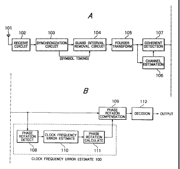
Fig.1 shows a block diagram of the first
embodiment of the p.resent OFDM packet communication
receiver, and it relates to claim 1.
In the embodiment, receiving means,
synchronization means, Fourier transform means,
channel estimation means, coherent detection means,
clock frequency error estimation means, and phase
rotation compensation means in claim 1 correspond
to a receiving circuit 102, a synchronization
circuit 103, a Fourier transform circuit 104, a
channel estimator 106, a coherent detection circuit
107, a clock frequency error estimation block 100,
and a phase rotation compensator 109, respectively.
An OFDM signal received by an antenna 101 is
applied to the receiving circuit 102, which carries
out a receiving process including frequency
conversion, filtering, orthogonal detection, and
A/D conversion. Then, the receiving circuit 102
provides complex baseband signal which is an output
of the receiving process.
An output signal of the receiving circuit 102
is applied to a sync:hronization circuit 103, which
detects carrier frequency error and OFDM symbol
timing by using a preamble signal for
synchronization (see Fig.44) included in the
29
CA 02346714 2001-04-06
complex baseband signal, and carries out carrier
frequency error compensation for the complex
baseband signal by using the detected carrier
frequency error.
The synchronization circuit 103 outputs a
complex baseband signal which is compensated
carrier frequency error, and a symbol timing
information.The output signals of the
synchronization circuit 103 are applied to a guard
interval removing circuit 104. The detected OFDM
symbol timing information is used to remove a guard
interval which exists each OFDM symbol of received
OFDM signals so that useful signal component in an
OFDM symbol is taken out.
The guard interval removing circuit 104
carries out FFT window process to an input complex
baseband signal by using symbol timing information
supplied by the synchronization circuit 103. In
other words, signal components having time width
equal to that of FF'r window are taken out from each
OFDM symbol of the complex baseband signals, so
that a guard interval is removed. The time width of
FFT window is equal to time difference between
symbol length of an OFDM symbol and length of a
guard interval.
A complex baseband signal whose guard interval
is removed by the guard interval removing circuit
104 is, for each OFDM symbol, applied to a Fourier
transform circuit 105, which carries out fast
Fourier transform to each OFDM symbol of input
CA 02346714 2001-04-06
complex baseband sigrials, so that the input signals
are divided into sigrial components of a plurality
of subcarriers.
Subcarrier signals divided by the Fourier
transform circuit 105 are applied to a coherent
detection circuit 107 and a channel estimator 106.
The channel estimator 106 estimates channel
condition, which eacti subcarrier signal is
transmitted, by usinci a preamble signals for
channel estimation (see Fig.44).
The channel estimation result which is
provided by the channel estimator 106 shows, for
instance, how each subcarrier is affected in phase
and amplitude by fading. The channel estimation
result is applied to a coherent detection circuit
107.
The coherent detection circuit 107 carries out
coherent detection by compensating the amplitude
fluctuation and the phase rotation, caused by
fading and others, of each subcarrier signal
supplied by the Four:ier transform circuit 105, by
using the channel estimation result of each
subcarrier supplied by the channel estimator 106.
An output signal of the coherent detection
circuit 107 is applied to a phase rotation
compensator 109, and a clock frequency error
estimation block 100. The latter is comprised of a
phase rotation detector 108, a clock frequency
error estimator 110, and a phase rotation
calculator 111.
31
CA 02346714 2001-04-06
For example, in the case where 16QAM
modulation scheme is used to modulate each
subcarrier, a signal after coherent detection is to
locate one of 16 reference signals S1 through S16
as shown in Fig. 45. However, when there exists a
sampling clock frequency error between a
transmitter and a receiver, the signals which are
coherent detected are subject to said phase
rotation, and output signals from the coherent
detection circuit 107 (e.g., R1 or R2 in Fig.45) do
not coincide with one of the reference signals S1
through S16. An amount of phase rotation of
detected signal depeinds upon each detected signal.
The phase rotation detector 108 in the clock
frequency error estiination block 100 detects phase
rotation or accumulated phase rotation of each
detected subcarrier signal. For instance, when an
output signal of the coherent detection circuit 107
is R1 in Fig.45, the phase rotation detector 108
finds the reference signal S3 which is the closest
to the input signal R1 among the reference signals
S1 through S16, and detects the phase difference ~
1 between the reference signal S3 and the input
signal R1. Further, when an output signal of the
coherent detection circuit 107 is R2 in Fig.45, the
phase rotation detector 108 finds the reference
signal S6 which is t:he closest to the input signal
R2 among the reference signals S1 through S16, and
detects the phase difference02 between the
reference signal S6 and the input signal R2.
32
CA 02346714 2001-04-06
The phase rotation caused by clock frequency
error is expressed by the equation (5). As the
phase rotation ( A 9 ) ( e . g . , Q S 1 or 0 2 in Fig. 45 )
caused by clock frequency error, elapsed time (t)
from the channel estimation, and frequency offset
(f) of each subcarrier from channel center
frequency are known, ratio (A x) of sampling clock
frequency error between a transmitter and a
receiver to a reference sampling clock frequency
can be calculated by using the equation (5).
Further, as the reference sampling clock frequency
(fr-LK) is known, amount of frequency error ( fRCLK-
fTILK) of sampling frequency between a transmitter
and a receiver can be calculated, from the ratio
0 x) of sampling frequency error between a
transmitter and a receiver to the reference
sampling frequency.
A clock frequency error estimator 110 receives
phase rotation information of each detected signal
supplied by the phase rotation detector 108 for
each OFDM symbol, and estimates ratio of sampling
clock frequency error between a transmitter and a
receiver to a reference sampling clock frequency
(i.e., clock frequency deviation), or it estimates
amount of clock frequency error between a
transmitter and a receiver (i.e., clock frequency
error), by using the equation (5).
The phase rotation calculator 111 receives the
clock frequency error or the clock frequency
deviation supplied by the clock frequency error
33
CA 02346714 2001-04-06
estimator 110, and calculates phase rotation of
each detected signal supplied by the coherent
detection circuit 107, caused by clock frequency
error..The phase rotation is calculated by using
the equation (5).
The phase rotation compensator 109 receives
detected signal from the coherent detection circuit
107, and carries out phase compensation process for
removing phase rotation caused by clock frequency
error according to phase rotation information
supplied by the phase rotation calculator 111.
A decision circuit 112 receives a phase
compensated detected signal supplied by the phase
rotation compensator 109. The decision circuit 112
discriminates a symbol of data signal in a detected
signal (see Fig.44), and provides the result as a
demodulated output. ighen 16 QAM modulation scheme
is used to modulate each subcarrier, the decision
circuit 112 discriminates which reference signal
among signals S1 thrieugh S16 each detected signal
coincides. Since phase rotation is compensated by
the phase rotation compensator 109 before a symbol
is discriminated, the symbol discrimination is
carried out free from clock frequency error. Thus,
accurate clock frequency synchronization which is
impossible in a prior art is realized. Further, as
mentioned above, clock frequency error compensation
is carried out through digital process, thus, no
complicated analog circuit is required, and power
consumption can be suppressed.
34
CA 02346714 2001-04-06
(Second embodiment)
The second embodiment which is a modification
of the first embodiment is described in accordance
with Fig.2. This embodiment is directed to claim
2. In Fig.2, the same numerals as those in Fig.2
show the same members.
In Fig.2, a clock frequency estimation block
200 comprises a weighting circuit 201, a smoothing
circuit 202, a phase rotation detector 203, a clock
frequency error estimator 110, and a phase rotation
calculator 111.
The weighting circuit 201 receives an output
signal of the coherent detection circuit 107 and
channel estimation result of each subcarrier
provided by the channel estimator 106. The
weighting circuit 201 detects phase rotation
information of an output of the coherent detection
circuit 107 from reference signal, and then, gives
an weight to the detected phase rotation
information according to the channel estimation
result provided by tlhe channel estimator 106.
For instance, when signal level of a
subcarrier obtained ]by the channel estimation
result is high, the phase rotation information of
the detected signal transmitted by the
corresponding subcarrier is weighted with a large
weight coefficient, and when signal level of a
subcarrier is low, the phase rotation information
is weighted with a small weight coefficient. The
CA 02346714 2001-04-06
above-mentioned weighting is advantageous that
succeeding circuits are affected little by phase
rotation of signal which has low signal level, and
accurate clock frequency error estimation can be
realized.
An output of the weighting circuit 201 is
applied to the smoothing circuit 202, which
calculates moving average of the weighted phase
rotation information on time axis for each
subcarrier, so that the weighted phase rotation is
smoothed. This smoothing operation functions to
avoid degradation of signal quality due to thermal
noise superimposed on a received signal in the
receiving circuit 102.
The phase rotation detector 203 receives an
output of the smoothing circuit 202, and detects
phase rotation (e.g., 0 i or 02 in Fig.45) or
accumulated phase rotation of each detected signal
caused by clock frequency error.
The clock frequency error estimator 110
estimates clock frequency deviation or clock
frequency error according to the equation (5) by
using the phase rotation information or the
accumulated phase rotation information provided by
the phase rotation detector 203.
The phase rotation calculator 111 calculates
phase rotation inforrnation of each detected signal,
which is an output of the coherent detection
circuit 107, according to the clock frequency error
information estimated by the clock frequency error
36
CA 02346714 2001-04-06
estimator 110. This phase rotation information is
obtained by the equation (5). An output of the
phase rotation calcu:Lator 111 is applied to the
phase rotation compensator 109.
When signal quality depends upon each
subcarrier, the weight to the phase rotation of a
subcarrier with good signal quality is high so that
the fading affects a little. Thus, the clock
frequency error is detected more accurately.
Further, the smoothing operation of the weighted
phase rotation on time axis suppresses the
affection by thermal noise and others, so that the
clock frequency error is detected further more
accurately. Thus, highly accurate clock frequency
compensation which is impossible in a prior art, is
obtained. Further, as the clock frequency error
compensation is carried out through digital
process, no complicated analog compensation circuit
is required, and powier consumption is suppressed.
(Third embodiment)
The third embodiment is described in
accordance with Fig.3, which is directed to claim
3, and is a modification of Fig.l. In Fig.3, the
same numerals as those in Fig.1 show the same
members.
In Fig.3, a clock frequency error estimation
block 300 comprises a pilot signal extractor 301, a
phase rotation detector 302, a clock frequency
error estimator 303, and a phase rotation
37
CA 02346714 2001-04-06
calculator 111.
This embodiment has the feature that a part of
subcarriers in an OFDM signal transmit a known
pilot signal.
A pilot signal extractor 301 receives output
signals of the coherent detection circuit 107, and
extracts pilot signals.
A phase rotation detector 302 receives the
extracted pilot signals, and detects phase rotation
or accumulated phase rotation of each pilot signal.
It should be noted that as a pilot signal is
known, the reference signal of the pilot signal is
also known. Therefore, when phase rotation of a
pilot signal is only detected, no discrimination of
reference signal is required, and thus, the signal
processing is simplified. Further, even when high
noise is added to a detected signal, no wrong
discrimination of a reference signal of a detected
signal occurs, and thus, phase rotation is detected
more accurately.
A clock frequency error estimator 303 receives
a phase rotation information or an accumulated
phase rotation information provided by the phase
rotation detector 302 for each detected signal, and
estimates clock frequency deviation or clock
frequency error.
A phase rotation. calculator 111 calculates
phase rotation, which is caused by clock frequency
error, of a detected signal provided by the
coherent detection circuit 107 for each detected
38
CA 02346714 2001-04-06
signal, according to clock frequency deviation or
clock frequency error estimated by the clock
frequency error estiinator 303. The phase rotation
is obtained based upon the equation (5).
The phase rotation compensator 109 compensates
phase rotation of an output of the coherent
detection circuit 107 due to clock frequency error,
according to phase rotation information provided by
the phase rotation calculator 111.
Thus, when known pilot signals are transmitted
by using a part of subcarriers in OFDM signals, a
clock frequency error is detected by using the
pilot signals. Thus, a clock frequency error can be
detected by using only a part of detected signals,
thus, a circuit for clock frequency error
estimation can be siinplified. Further, even when
high noise is added to a received signal, no wrong
discrimination of a reference signal of a detected
signal occurs, and thus, a clock frequency error is
detected more accurately.
Thus, highly accurate clock frequency
compensation which is impossible in a prior art can
be realized with a simple circuit. Further, as a
clock frequency error is compensated through
digital process, no complicated analog compensation
circuit is required, and thus, power consumption is
suppressed.
(Fourth embodiment)
The fourth embodiment of the present invention is
39
CA 02346714 2001-04-06
described in accordance with Fig.4 which is
directed to claim 4 and is a modification of Fig.1.
The same numerals in Fig.4 show the same members as
those in Fig.1.
A clock frequency estimation block 400 in
Fig.4 comprises a pilot signal extractor 401, an
weighting circuit 402, a smoothing circuit 403, a
phase rotation detector 404, a clock frequency
error estimator 405, and phase rotation calculator
111.
This embodiment has feature that known pilot
signals are transmitted by using a part of
subcarriers included in OFDM signals.
The pilot signal extractor 401 receives output
signals of the coherent detection circuit 107, and
extracts only pilot signal components.
The weighting circuit 402 takes the phase
rotation information of the pilot signals extracted
by the pilot signal extractor 401 and gives a
weight to the phase rotation information according
to the channel estimation result which is the
output of the channel estimator 106.
For instance, when signal level of a
subcarrier obtained by the channel estimation
result is high, the phase rotation information of
the pilot signal transmitted by the corresponding
subcarrier is weighted with a large weight
coefficient, and when signal level of a subcarrier
is low, the phase rotation information is weighted
with a small weight coefficient. The above-
CA 02346714 2001-04-06
mentioned weighting is advantageous that succeeding
circuits are affecteci little by phase rotation of
pilot signal which has low signal level, and
accurate clock frequency error estimation can be
realized
An output of the weighting circuit 402 is
applied to the smoothing circuit 403, which
calculates moving average of the weighted phase
rotation along time axis for each subcarrier. Thus,
the smoothing circuit 403 smoothes the weighted
phase rotation inforination. The smoothing operation
removes the degradation of signal quality due to
the effect of therma:L noise and others added at the
receiving circuit 102.
The phase rotation detector 404 receives the
weighted and smoothed phase rotation information,
and detects the phase rotation (e.g., 0 1 or 0 2 in
Fig.45) or the accumulated phase rotation caused by
the clock frequency error for each pilot signal.
The clock frequency error estimator 405
calculates the clock frequency deviation or the
clock frequency erro:r according to the equation (5)
by using the phase rotation or the accumulated
phase rotation of each pilot signal.
The phase rotation calculator 111 calculates
the amount of phase rotation of the coherent
detected signal provided by the coherent detection
circuit 107 according to the clock frequency error
information provided by the clock frequency error
estimator 405. This phase rotation is calculated
41
CA 02346714 2001-04-06
according to said equation (5). An output of the
phase rotation calculator 111 is applied to the
phase rotation compensator 109.
As described above, when pilot signals are
transmitted by using a part of subcarriers in OFDM
signals, a clock frequency error is detected by
using the pilot signals, thus, the clock frequency
is detected by using only a part of OFDM signals,
and thus, the circuit structure is simplified.
Further, even when high noise is added to a
coherently detected signal, a clock frequency error
is detected accurately, since reference signal of
each detected signal is discriminated correctly.
Further, when signal quality depends upon each
subcarrier, the phase rotation detected by using a
pilot signal on a high subcarrier which is in good
transmission quality has large weight so that the
affection by fading is decreased, and a clock
frequency error is accurately detected. Further,
the smoothed phase rotation along time axis
suppresses the affection by thermal noise and
others, and thus, the clock frequency error is
detected more accurately.
Thus, the accurate clock frequency
compensation is carried out by using a simple
circuit, although it has been impossible in a prior
art. Further, as the clock frequency error
compensation is carried out in a digital circuit,
no complicated analog compensation circuit is
required, and the power consumption is saved.
42
CA 02346714 2001-04-06
(Fifth embodiment)
Fig.5 shows fifth embodiment, which is a
modification of Fig.l, and is directed to claim 5.
In Fig.5, the same numerals as those in Fig.1 show
the same members.
Receiving means, Synchronization means,
Foufier transform means, channel estimation means,
coherent detection means, clock frequency error
estimation means, and phase rotation compensation
means in claim 5 correspond, respectively, a
receiving circuit 102, a synchronization circuit
103, a Fourier transform circuit 105, a channel
estimator 106, a coherent detection circuit 107, a
clock frequency error estimation block 500, and a
phase rotation compensator 109 in Fig.5.
The clock frequency error estimation block 500
in Fig.5 comprises a phase rotation detector 501, a
clock frequency error estimator 502, and a phase
rotation calculator 1303.
The phase rotation detector 501 receives an
output of the phase rotation compensator 109, and
detects the amount of phase rotation of coherently
detected signal for each OFDM symbol, and each
subcarrier. The operation of the phase rotation
detector 501 is essentially the same as that of the
phase rotation detector 108 in Fig.1.
The clock frequency error estimator 502
estimates clock frequency deviation or clock
frequency error by using phase rotation information
43
CA 02346714 2001-04-06
of detected signal supplied by the phase rotation
detector 501 until reception of the current OFDM
symbol.
The phase rotation calculator 503 receives the
clock frequency deviation or the clock frequency
error supplied by the clock frequency error
estimator 502, and calculates phase rotation of a
detected signal caused by the clock frequency error
which is supplied by the coherent detection circuit
107 for each detection signal. The amount of phase
rotation can be calculated according to said
equation (5).
The phase rotation compensator 109 receives a
detected signal from the coherent detection circuit
107 and compensates phase rotation of the detected
signal caused by clock frequency error according to
phase rotation information supplied by the phase
rotation calculator 503.
The modification of Fig.5 has a feature that
phase rotation is detected by using compensated
output of the phase rotation compensator 109, while
the embodiment of Fig.1 detects phase rotation by
using uncompensated signal of an input of the phase
rotation compensator 109.
Thus, the embodiment of Fig.5 compensates
phase rotation of a coherently detected signal and
then discriminates which reference signal each
detected signal corresponds, as is the case of
Fig.1, and thus, it can discriminate a signal
without being affected by clock frequency error,
44
CA 02346714 2001-04-06
and provide highly accurate clock frequency error
compensation which is impossible in a prior art.
Further, as compensation process is carried out
through digital process, no complicated analog
compensation circuit is required, and power
consumption is suppressed.
(Sixth embodiment)
Fig.6 shows sixth embodiment, which is a
modification of Fig.5, and is directed to claim 6.
The same numerals in Fig.6 as those in Fig.5 show
the same members.
In Fig.6, a clock frequency error estimation
block 600 comprises a weighting circuit 601, a
smoothing circuit 602, a phase rotation detector
603, a clock frequency error estimator 502, and a
phase rotation calculator 503.
The clock frequency error estimator 502
estimates clock frequency deviation or clock
frequency error by using the phase rotation
information of a detected signal supplied by the
phase rotation detector 603 until the reception of
the current OFDM symbol.
The weighting ci_rcuit 601 receives an output
of the phase rotation compensator 109 and detects
phase rotation of the phase compensated signal from
a reference signal, then, it gives a weight to the
phase rotation information according to channel
estimation result supplied by the channel estimator
106, for each coherently detected signal.
CA 02346714 2001-04-06
For instance, when signal level of a
subcarrier obtained by the channel estimation
result is high, the phase rotation information of
the detected signal transmitted by the
corresponding subcar:rier is weighted with a large
weight coefficient, and when signal level of a
subcarrier is low, t:he phase rotation information
is weighted with a small weight coefficient. The
above-mentioned weig:hting is advantageous that
succeeding circuits are affected little by phase
rotation of the detected signal which has low
signal level, and accurate clock frequency error
estimation can be realized.
The weighted phase rotation information is
applied to the smoothing circuit 602, which carries
out the moving average of the weighted phase
rotation information for each subcarrier along time
axis, so that the weighted phase rotation
information is smoothed. The smoothing operation
removes degradation of signal quality which is
degraded in a receiving circuit 2 by thermal noise
and others.
The phase rotation detector 603 receives
weighted and smoothed phase rotation information,
and detects phase rotation caused by clock
frequency error.
An output of the phase rotation detector 603
is applied to the clock frequency error estimator
502 for estimation of clock frequency deviation or
clock frequency error.
46
CA 02346714 2001-04-06
When signal quality depends upon each
subcarrier, the effect by fading is suppressed, as
described above, by assigning large weight to the
phase rotation which relates to a subcarrier having
good signal quality, and clock frequency error can
be detected more accurately. Further, as the
smoothing operation along time axis suppresses the
effect by thermal noise and others, clock frequency
error is detected further more accurately. Thus,
highly accurate clock frequency error compensation
which is impossible in a prior art is realized.
Further, as clock frequency error compensation is
implemented through digital process, no complicated
analog compensation circuit is required, and thus,
power consumption is saved.
(Seventh embodiment)
Fig.7 shows seventh embodiment, which is a
modification of Fig.5 and is directed to to claim
7. In Fig.7, the same numerals as those in Fig.5
show the same members.
In Fig.7, a clock frequency error estimation
block 700 comprises a pilot signal extractor 701, a
phase rotation detector 702, a clock frequency
error estimator 703 and a phase rotation calculator
503.
It is assumed in Fig.7 that known pilot
signals are transmitted by using a part of
subcarriers in OFDM signals.
The pilot signal extractor 701 receives phase
47
CA 02346714 2001-04-06
rotation compensated output of the phase rotation
compensator 109, and extracts pilot signal
components in detected signals.
The phase rotation detector 702 receives a
pilot signal component, and detects phase rotation
or accumulated phase rotation in the pilot signal
component.
As a pilot signal is a known signal, a
reference signal relating to a pilot signal is also
known. Therefore, when phase rotation of a pilot
signal is detected, no discrimination of a
reference signal is required, and thus, signal
processing is simplified. Further, even when high
noise is added to a coherently detected signal, a
reference signal can be correctly discriminated,
and thus, phase rotation can be detected more
accurately.
The clock frequency error estimator 703
receives an output of the phase rotation detector
702, and estimates clock frequency deviation or
clock frequency erro:r.
An output of the clock frequency error
estimator 703 is applied to the phase rotation
calculator 503 which calculates phase rotation in
each coherently detected signal due to clock
frequency error.
When known pilot signals are transmitted by
using a part of subcarriers in OFDM signals, a
clock frequency error estimator can be simplified,
as clock frequency error can be detected by using
48
CA 02346714 2001-04-06
pilot signals which are only a part of detected
signals, and further, clock frequency error can be
detected accurately as reference signal is
correctly discriminated even under high noise
condition. Thus, high accurate clock frequency
compensation which is impossible in a prior art is
realized. Further, as clock frequency error
compensation process is carried out through a
digital circuit, no complicated analog circuit is
required, and power consumption is saved.
(Eighth embodiment)
Fig.8 shows eighth embodiment, which is a
modification of Fig.5, and is directed to claim 8.
The same numerals in Fig.8 as those in Fig.5 show
the same members.
A clock frequency error estimation block 800
comprises a pilot signal extractor 801, a weighting
circuit 802, a smoothing circuit 803, a phase
rotation detector 804, a clock frequency error
estimator 805, and a phase rotation calculator 503.
It is assumed in Fig.8 that known pilot
signals are transmitted by using a part of
subcarriers in OFDM signals.
The pilot signal extractor 801 receives
coherently detected and phase compensated signals
from the phase rotation compensator 109, and
extracts pilot signal components in the detected
signals.
The weighting circuit 802 receives the
49
CA 02346714 2001-04-06
extracted pilot signal, which has phase rotation
information of a pilot signal, and then, gives a
weight to said phase rotation information according
to channel estimation result provided by the
channel estimator 106.
For instance, when signal level of a
subcarrier obtained by the channel estimation
result is high, the :phase rotation information of
the pilot signal transmitted by the corresponding
subcarrier is weighted with a large weight
coefficient, and when signal level of a subcarrier
is low, the phase rotation information is weighted
with a small weight coefficient. The above-
mentioned weighting is advantageous that succeeding
circuits are affected little by phase rotation of a
pilot signal which has low signal level, and
accurate clock frequency error estimation can be
realized.
An output of the weighting circuit 802 is
applied to the smoothing circuit 803, which carries
out moving average o:f the weighted phase rotation
information along time axis for each subcarrier, so
that the weighted phase rotation information is
smoothed. The smoothing operation removes
degradation of signal quality due to thermal noise
and others in the receiving circuit 102.
The phase rotation detector 804 detects phase
rotation of the weighted and smoothed pilot signal.
The clock frequency error estimator 805
estimates clock frequency deviation or clock
CA 02346714 2001-04-06
frequency error by using the detected phase
rotation according to the equation (5).
The clock frequency deviation or the clock
frequency error estimated by the clock frequency
error estimator 805 is applied to the phase
rotation calculator 503.
As described above, when known pilot signals
are transmitted by using a part of subcarriers in
OFDM signals, clock frequency error can be detected
effectively by using only a part of detected
signals, and thus, structure of a clock frequency
error estimator can ibe simplified. Further, even
when high thermal noise is added to a coherently
detected signal, a reference signal of the related
signal is discriminated correctly, and thus, the
accuracy of the clock frequency error is improved.
Further, even when signal quality depends upon
each subcarrier, clock frequency error can be
detected accurately, by mitigating the effect of
fading by giving large weight to the phase rotation
information relating to a pilot signal with good
transmission quality. Further, as the smoothing
operation along time axis suppresses the effect by
thermal noise and others, clock frequency error is
detected further more accurately. Thus, highly
accurate clock frequency error compensation which
is impossible in a prior art is accomplished.
Further, as the cloc:k frequency error compensation
is carried out through digital process, and
therefore, no complicated analog circuit is
51
CA 02346714 2001-04-06
required, and power consumption is saved.
(Ninth embodiment)
Fig.9 shows ninth embodiment which is directed
to claim 9.
Receiving means, synchronization means,
Fourier transform means, channel estimation means,
coherent detection means, residual carrier
frequency error est.iination means, phase rotation
estimation means, and phase rotation compensation
means in claim 9 correspond, respectively, to a
receiving circuit 10:2, a synchronization circuit
901, a Fourier transform circuit 105, a channel
estimator 106, a coherent detection circuit 107, a
residual carrier frequency error detector 902, a
phase rotation estimator 904, and a phase rotation
compensator 109.
It is assunied in Fig.9 that sampling clock
frequency is synchronized with carrier frequency in
a transmitter which transmits OFDM signals.
Further, a receiver :in Fig.9 controls so that
sampling clock frequency in a receiver is
synchronized with carrier frequency in a receiver.
In the current embodiment, carrier frequency and
sampling clock frequency are generated by a common
single generator, and therefore, sampling clock
frequency is inherently synchronized with carrier
frequency.
An OFDM signal received by an antenna 101 is
applied to a receiving circuit 102, which carries
52
CA 02346714 2001-04-06
out receiving process including frequency
conversion, filtering, orthogonal detection, A/D
conversion and others to the received OFDM signals,
and provides baseband signals in complex form as
output signals.
The complex baseband signal from the receiving
circuit 102 is applied to a synchronization circuit
901, which detects OFDM symbol timing and carrier
frequency error by using a preamble for
synchronization (Fig.44) included in the complex
baseband signals. By using the carrier frequency
error information, the synchronization circuit 901
carries out to compeinsate the carrier frequency
error for the complex baseband signals.
The synchronization circuit 901 provides
complex baseband signals which the carrier
frequency error is compensated, the symbol timing
information, and the detected carrier frequency
error information. The complex baseband signals and
the symbol timing information are applied to the
guard interval removing circuit 104, and the
carrier frequency er:ror information is applied to a
phase rotation estimator 904. The symbol timing
information is necessary for removing a guard
interval of each received OFDM symbol, and
extracting useful data component from each symbol.
The guard interval removing circuit 104
carries out FFT window process to the complex
baseband signals according to the symbol timing
information from the synchronization circuit 901.
53
CA 02346714 2001-04-06
In other words, a guard interval is removed by
extracting only signal components having time width
equal to time width of FFT window for each OFDM
symbol in complex baseband signals. The time width
of FFT window is equal to the difference between
OFDM symbol length and a guard interval length.
The complex baseband signal which is free from
a guard interval is applied to a Fourier transform
circuit 105 for each OFDM symbol. The Fourier
transform circuit 105 carries out fast Fourier
transform to each OF:DM symbol so that the input
signals are divided into subcarrier signals.
The divided subcarriers are applied to a
coherent detection circuit 107 and a channel
estimator 106. The channel estimator 106 estimates
condition of a channiel which each subcarrier is
transmitted by using a preamble for channel
estimation (Fig.44).
An output of the channel estimator 106, i.e.,
channel estimation result, provides how amplitude
and phase of each subcarrier is affected by fading.
An output of the channel estimator 106 is applied
to a coherent detection circuit 107.
The coherent detection circuit 107 carries out
coherent detection process to the complex baseband
signals from the Fourier transform circuit 105 by
compensating amplitude fluctuation and phase
rotation due to fading, carrier frequency error and
others for each subcarrier by using the channel
estimation result provided by the channel estimator
54
CA 02346714 2001-04-06
106.
An output of the coherent detection circuit
107 is applied to a residual carrier frequency
error detector 902 and a phase rotation compensator
109. The residual ca:rrier frequency error detector
902 detects residual carrier frequency error by
detecting phase rotation caused by residual carrier
frequency error in a coherently detected signals.
For example, in the case where 16QAM
modulation scheme is used to modulate each
subcarrier, a signal after coherent detection is to
locate one of 16 reference signals Si through S16
as shown in Fig. 45. However, when there exists a
sampling clock frequency error between a
transmitter and a receiver, the signals which are
coherent detected are subject to said phase
rotation as shown in the equation (5) and (6), and
output signals from the coherent detection circuit
107 (e.g., R1 or R2 in Fig.45) do not coincide with
one of the reference signals Sl through S16.
The phase rotation caused by carrier frequency
error is uniform to a signal component of all the
detected signals in an OFDM symbol, as shown in the
equation (6). Further, as OFDM symbol duration is
fixed, phase rotation per one OFDM symbol is
proportional to residual carrier frequency error.
Therefore, the residual carrier frequency error
detector 902 detects residual carrier frequency
error according to the equation (6), by detecting
phase rotation which is common to all the
CA 02346714 2001-04-06
subcarriers in a certain OFDM symbol, or by
detecting accumulated phase rotation from channel
estimation until a current OFDM symbol.
In practice, phase rotation of each subcarrier
from a reference sigrial is detected in a certain
OFDM symbol. For instance, when a detected signal
from the coherent detection circuit 107 is R1 in
Fig.45, the residual carrier frequency error
detector 902 detects the phase difference 0 1
between the detected signal Rl and the reference
signal S3 which is the closest to the detected
signal R1 among the reference signals Sl through
S16. Further, when a detected signal is R2 in
Fig.45, the residual carrier frequency error
detector 902 detects the phase difference 0 2
between the detected signal R2 and the reference
signal S6 which is the closest to the detected
signal R2.
The detected phase rotation includes not only
the phase rotation caused by residual carrier
frequency error showri in the equation (6), but also
the phase rotation caused by clock frequency error
shown in the equatiori (5). Therefore, in order to
detect the phase rotation which is uniform to all
the subcarriers in a certain OFDM symbol caused by
the residual carrier frequency error, the carrier
frequency error detector 902 takes an average of
the phase rotations of all the subcarriers in the
OFDM symbol.
The phase rotation caused by clock frequency
56
CA 02346714 2001-04-06
error is proportional to frequency offset between
channel center frequency and current subcarrier
frequency as shown in the equation (5). Therefore,
when phase rotations of all the subcarriers in an
OFDM symbol are averaged, phase rotations of the
subcarriers symmetrical to channel center frequency
are cancelled with each other, and thus, only the
phase rotation of the equation (6) due to the
residual carrier frequency error is obtained. By
using the phase rotation information thus obtained,
the residual carrier frequency error is calculated
according to the equation (6). The residual carrier
frequency error detector 902 provides the thus
calculated residual carrier frequency error
information.
The phase rotation estimator 904 receives the
residual carrier frequency error information from
the residual carrier frequency error detector 902,
and the carrier frequency error information from
the synchronization circuit 901. Then, the phase
rotation estimator 904 estimates phase rotation due
to clock frequency error for each detected signal.
In the embodiment, it is assumed that carrier
frequency and samplirig clock frequency are
synchronized with eac:h other in a transmitter, and
carrier frequency anci sampling clock frequency in a
receiver are synchronized with each other. With
that assumption, the ratio (A x) of the sampling
clock frequency error between a transmitter and a
receiver to a referer.ice sampling clock frequency is
57
CA 02346714 2001-04-06
equal to the ratio of the carrier frequency error
between a transmitter and a receiver to a reference
carrier frequency. Thus, the following equation is
satisfied.
A X = ( f RCLK f TCLK )/ f C::,K f/ f RF 1 f RRF f TRF )/ f RF (7 )
where;
fTRF carrier frequency in a transmitter
fRRF carrier frequency in a receiver
fRF reference carrier frequency
Accordingly, by inserting the equation (7)
into the equation (5), the phase rotation A 9 of a
detected signal due to clock frequency error
between a transmitter and a receiver is expressed
as follows.
A e - 27r * f * t fRRF f TRF ) / f RF (8)
Thus, the phase rotation 0 B due to clock
frequency error between a transmitter and a
receiver is obtained based upon the equation (8)
according to carrier frequency error information
from the synchronization circuit 901 and residual.
carrier frequency error information from the
residual carrier frequency error detector 902. By
the way, although the phase rotation A 8 might be
obtained based upon the equation (8) only by using
the clock frequency error information between a
transmitter and a receiver, the use of the residual
carrier frequency error information improves the
accuracy of the detected phase rotation.
It should be noted in the equation (8) that
the phase rotation A 0 due to clock frequency error
58
CA 02346714 2001-04-06
between a transmitter and a receiver depends upon
each subcarrier and each OFDM symbol. Therefore,
the phase rotation estimator 904 estimates the
phase rotation of a coherently detected signal
based upon the equation (8) due to clock frequency
error between a transmitter and a receiver by using
both an output of the synchronization circuit 901
and an output of the residual carrier frequency
error detector 902.
The phase compensator 903 carries out the
phase compensation for each coherently detected
signals from the coherent detection circuit 107
according to the phase rotation information for
each detected signals from the phase rotation
estimator 904.
An output of the phase rotation compensator
109 is applied to a decision circuit 112, which
discriminates a symbol for data signals (Fig.44),
and provides a discr_Lminated result as a
demodulated output. When 16 QAM modulation scheme
is used to modulate each subcarrier, the decision
circuit 112 discriminates which reference signal S1
through S16 a detected signal corresponds. Since
the phase rotation is compensated accurately, the
signal can be discriminated with no affection of
clock frequency error. Thus, a highly accurate
clock frequency erroi- compensation which is
impossible in a prior art is obtained. Further, as
clock frequency erroi- compensation is carried out
through digital process, no complicated analog
59
CA 02346714 2001-04-06
compensation circuit is required, and power
consumption is saved.
(Tenth embodiment)
Fig.10 shows tenth embodiment, which is a
modification of Fig.9, and is directed to claim 10.
The same numerals in Fig.10 as those in Fig.9 show
the same members.
Fig.10 embodiment comprises a weighting
circuit 1001 and a smoothing circuit 1002. The
operation of a residual carrier frequency error
detector 1003 is essentially the same as that of
the residual carrier frequency error detector 902.
It is assumed in Fig.10 that carrier frequency
and clock frequency are synchronized with each
other in a transmitter, and further, clock
frequency in a receiver is controlled so that it
synchronizes with carrier frequency.
A weighting circuit 1001 receives an output of
the coherent detection circuit 107, an output of
the channel estimator 106, and an output of a phase
rotation estimator 904.
The weighting circuit 1001 receives a part or
all of the detected signals of the coherent
detection circuit 107. The weighting circuit 1001
compensates phase rotation in the detected signal
caused by clock frequency error by using the phase
rotation information provided by the phase rotation
estimator 904, and then, the weighting circuit 1001
gives a weight to the phase rotation information
CA 02346714 2001-04-06
according to an output of the channel estimator
106.
For instance, when signal level of a
subcarrier obtained by the channel estimation
result is high, the phase rotation information of
the signal transmitted by the corresponding
subcarrier is weighted with a large weight
coefficient, and when signal level of a subcarrier
is low, the phase rotation information is weighted
with a small weight coefficient. The above-
mentioned weighting is advantageous that residual
carrier frequency error estimator are affected
little by phase rotation of the signal which has
low signal level, and accurate residual carrier
frequency error est.irnation can be realized.
The phase rotation information weighted by the
weighting circuit 1001 is applied to the smoothing
circuit 1002, which carries out moving average of
the weighted phase rotation information for each
subcarrier along time axis. Thus, the smoothing
circuit 1002 smoothes the weighted phase rotation
information. The smoothing operation removes the
signal degradation due to thermal noise and others
added to a received signal in the receiving circuit
102.
The residual carrier frequency error detector
1003 receives the weighted and smoothed phase
rotation information, and calculates residual
carrier frequency error according to the equation
(6) by detecting the phase rotation caused by
61
CA 02346714 2001-04-06
residual carrier frequency error in the weighted
and smoothed phase rotation information. The
operation of the residual carrier frequency error
detector 1003 is essentially the same as that of
the residual carrier frequency error detector 902.
The phase rotation estimator 904 estimates
phase rotation caused by clock frequency error for
each detected signal according to carrier frequency
error information from the synchronization circuit
901 and residual caririer frequency error
information from the residual carrier frequency
error detector 1003.
When signal quality depends upon each
subcarrier, the effect of fading is decreased by
assigning large weight to the phase rotation
information relating to a subcarrier with good
communication quality, and the residual carrier
frequency error is accurately detected. Further,
with the averaging of the phase rotation along time
axis, further accurate residual carrier frequency
error is obtained by suppressing effect of thermal
noise and others. Thus, a highly accurate clock
frequency error compensation which is impossible in
a prior art is obtained, and further, the
compensation for clock frequency error is carried
out through digital process, no complicated analog
circuit is required, and power consumption is
saved.
(Eleventh embodiment)
62
CA 02346714 2001-04-06
Fig.11 shows eleventh embodiment, which is a
modification of Fig.9 and is directed to claim 11.
The same numerals in Fig.11 as those in Fig.9 show
the same members.
The embodiment of Fig.11 has a pilot signal
extractor 1101. The operation of a residual carrier
frequency error detector 1102 is essentially the
same as that of the residual carrier frequency
error detector 902.
It is assumed in Fig.11 that known pilot
signals are transmitted by using a part of
subcarriers in OFDM signals.
Further, it is assumed in Fig.11 that carrier
frequency and clock frequency are synchronized with
each other in a transmitter, and clock frequency is
controlled in a receiver so that it synchronizes
with carrier frequency.
The pilot signal extractor 1101 receives
output signals of the coherent detection circuit
107, and extracts signal components of pilot
signals in said output signals.
The residual carrier frequency error detector
1102 receives said pilot signal, and detects phase
rotation for each detected signal or accumulated
phase rotation in the detected signal which is
common to all detected signals in an OFDM symbol.
As a pilot signal is a known signal, a
reference signal (e.g., one of S1 through Si6 in
Fig.45) corresponding to the pilot signal is also
known. Therefore, when phase rotation of a pilot
63
CA 02346714 2001-04-06
signal is only detected, no reference signal
relating to the pilot signal is necessary to be
discriminated, and the signal processing in the
residual carrier frequency error detector 1102 is
simplified. Further, even when noise component is
added to a detected signal, a reference signal
relating to the detected signal is correctly
discriminated, and thus, the phase rotation is
accurately detected.
The residual carrier frequency error detector
1102 obtains residual carrier frequency error
according to the equation (6) from the detected
phase rotation or accumulated phase rotation. The
operation of the residual carrier frequency error
detector 1102 is essentially the same as that of
the residual carrier frequency error detector 902.
An output of the residual carrier frequency error
detector 1102 is applied to the phase rotation
estimator 904.
As described above, when pilot signals which
are known are transmitted, residual carrier
frequency error can be detected by using pilot
signals which are only a part of the detected
signals, and thus, the structure of the residual
carrier frequency error detection means is
simplified. Further, even when noise component is
added to a detected signal, the detected signal is
correctly discriminated, and therefore, the
residual carrier frequency error is detected
accurately.
64
CA 02346714 2001-04-06
Thus, a highly accurate clock frequency
compensation which is impossible in a prior art is
obtained. And further, as the clock frequency error
compensation is carried out through digital
process, no complicated analog circuit is required,
and power consumption is saved.
(Twelfth embodiment)
Fig.12 shows twelfth embodiment, which is a
modification of Fig.9, and is directed to claim 1.2.
The same numerals in Fig.12 as those in Fig.9 show
the same members.
The embodiment of Fig.12 comprises a pilot
signal extractor 120:1, a weighting circuit 1202, a
smoothing circuit 1203, and a residual carrier
frequency error detector 1204. The operation of the
residual carrier frequency error detector 1204 is
essentially the same as that of the residual
carrier frequency error detector 902.
It is also assumed in Fig.12 that known pilot
signals are transmitted by using a part of
subcarriers.
Further, it is assumed that carrier frequency
and clock frequency are synchronized with each
other in a transmitter, and clock frequency in a
receiver is synchronized with carrier frequency.
The pilot signal extractor 1201 extracts pilot
signals in output signals of the coherent detection
circuit 107.
The weighting circuit 1202 receives a pilot
CA 02346714 2001-04-06
signal extracted by the pilot signal extractor
1201, a channel estimation result estimated by the
channel estimator 106, and phase rotation
information provided by the phase rotation
estimator 904. The weighting circuit 1202
compensates, first, phase rotation of a detected
signal caused by clock frequency error by using
phase rotation inforination of the corresponding
detected signal provided by the phase rotation
estimator 904, and diatects phase rotation of the
phase compensated siignal from a reference signal.
Then, the weighting circuit 1202 gives a weight to
the phase rotation information according to a
channel estimation result provided by the channel
estimator 106.
For instance, when signal level of a
subcarrier obtained ]by the channel estimation
result is high, the phase rotation information of
the pilot signal transmitted by the corresponding
subcarrier is weighted with a large weight
coefficient, and when signal level of a subcarrier
is low, the phase rotation information is weighted
with a small weight coefficient. The above-
mentioned weighting is advantageous that succeeding
circuits are affected little by phase rotation of
pilot signal which has low signal level, and
accurate residual carrier frequency error
estimation can be realized.
The phase rotation information weighted by the
weighting circuit 1202 is applied to a smoothing
66
CA 02346714 2001-04-06
circuit 1203, which carries out moving average of
the weighted phase rotation information for each
subcarrier along time axis. Thus, the smoothing
circuit 1203 smoothes the weighted phase rotation
information. The smoothing operation removes signal
degradation caused by thermal noise and others in
the receiving circuit 102.
The residual carrier frequency error detector
1204 receives an output of the smoothing circuit
1203, detects phase rotation caused by residual
carrier frequency error, and calculates residual
carrier frequency error. The operation of the
residual carrier frequency error detector 1204 is
essentially the same as that of the residual
carrier frequency error detector 902. An output of
the residual carrier frequency error detector 1204
is applied to the phase rotation estimator 904.
As described above, as pilot signals are
transmitted, and residual carrier frequency error
can be efficiently detected by using pilot signals
which are only a part of the coherent detected
signals, the circuit structure of residual carrier
frequency error detection means is simplified.
Further, even when noise is added to a detected
signal, the reference signal relating to the
detected signal. is correctly discriminated, and
therefore, the residual carrier frequency error can
be accurately detected.
Further, when communication quality depends
upon each subcarrier, the weight relating to a
67
CA 02346714 2001-04-06
subcarrier with good signal quality is selected
large, so that the effect by fading is decreased,
and therefore, the residual carrier frequency error
is further accurately detected. Further, as the
smoothing operation of phase rotation along time
axis suppresses the effect by thermal noise and
others, residual carrier frequency error is
detected further more accurately. Thus, a highly
accurate clock frequency error compensation which
is impossible in a prior art is realized. And
further, as the clock frequency error compensation
is carried out through digital process, no
complicated analog circuit is required, and power
consumption is saved.
(Thirteenth embodiment)
Fig.13 shows thirteenth embodiment, which is a
modification of Fig.9, and is directed to claim 13.
The same numerals in Fig.13 as those in Fig.9 show
the same members.
In claim 13, receiving means, synchronization
means, Fourier transform means, channel estimation
means, coherent detection means, first phase
rotation estimation imeans, first phase rotation
compensation means, residual carrier frequency
error estimation means, second phase rotation
estimation means, and second phase rotation
compensation means correspond, respectively, to a
receiving circuit 102, a synchronization circuit
901, a Fourier transform circuit 105, a channel
68
CA 02346714 2001-04-06
estimator 106, a coherent detection circuit 107, a
phase rotation estimator 904, a phase rotation
compensator 1302, a:residual carrier frequency
error detector 902, a phase rotation estimator 904,
and a phase rotation compensator 903.
It is also assumed in Fig.13 that sampling
clock frequency is synchronized with carrier
frequency in a transmitter, and a receiver controls
sampling clock frequiency so that it synchronizes
with carrier frequency.
In Fig.13, an OFDM packet communication
receiver comprises two independent phase rotation
estimators 1301 and 904, and two independent phase
rotation compensators 903, and 1302. The phase
rotation estimator 1301 estimates phase rotation of
a coherently detected signal caused by clock
frequency error by using carrier frequency error
information from a synchronization circuit 901.
As sampling clock frequency in a transmitter
is synchronized with carrier frequency, and
sampling clock frequency in a receiver is
synchronized with carrier frequency, the phase
rotation caused by clock frequency error can be
obtained by using the carrier frequency error
information according to the equation (6). As phase
rotation depends upon each detected signal, the
phase rotation estimator 1301 calculates phase
rotation of each detected signal.
The phase rotation compensator 1302 receives a
coherently detected signal provided by the coherent
69
CA 02346714 2001-04-06
detection circuit 107, and compensates phase
rotation caused by c:Lock frequency error of the
coherently detected signal according to phase
rotation information of the related coherently
detected signal estimated by the phase rotation
estimator 1301.
However, in an actual receiver, a
synchronization circuit 901 can not detect and
compensate carrier firequency error completely
accurately due to thermal noise added to a received
signal in a receiving circuit 102, and therefore,
complex baseband signal provided by the
synchronization circuit 901 includes residual
carrier frequency error. Since the phase rotation
compensator 1302 compensates phase rotation
estimated by the phase rotation estimator 1301
according to carrier frequency error information
provided by the synchronization circuit 901, the
output of the phase rotation compensator 1302 still
includes phase rotat:ion caused by residual clock
frequency error corresponding to the residual
carrier frequency error.
In order to solve the above problem, the
current embodiment has another phase rotation
compensator 903 for compensating residual phase
rotation caused by residual clock frequency error
which is a part of phase rotation caused by clock
frequency error.
The residual carrier frequency error detector
902 receives an output of the first phase rotation
CA 02346714 2001-04-06
compensator 1302, and detects residual carrier
frequency error included in said output. The
residual carrier frequency error is detected by
detecting the phase rotation of each coherently
detected signal caused by residual carrier
frequency error. The operation of the residual
carrier frequency error detector 902 has already
been described.
The phase rotation estimator 904 estimates
said residual phase rotation in an output of the
phase rotation compeiisator 1302 according to the
residual carrier frequency error information
provided by the residual carrier frequency error
detector 902, for each detected signal.
As it is assumed in the current embodiment
that sampling clock frequency in a transmitter is
synchronized with carrier frequency, and sampling
clock frequency in a receiver is synchronized with
carrier frequency, the phase rotation caused by
clock frequency error can be obtained according to
the equation (8) by usi.ng the residual carrier
frequency error detected by the residual carrier
frequency error detector 902. As phase rotation
depends upon each detected signal, the phase
rotation estimator 904 calculates phase rotation
for each detected signal.
The phase rotation compensator 903 carries out
the phase rotation compensation process so that the
phase rotation in an output of the first phase
rotation compensator 1302 is removed, according to
71
CA 02346714 2001-04-06
phase rotation inforrnation of each coherently
detected signal provided by the phase rotation
estimator 904. The second phase rotation
compensation removes residual phase rotation caused
by clock frequency error which can not be removed
in the first phase rotation compensator 1302.
The phase rotation compensators 1302 and 903
accurately compensate phase rotation caused by
clock frequency error between a transmitter and a
receiver for each detected signal, before a
detected signal is discriminated which reference
signal corresponds. 'Pherefore, the decision circuit
112 can discriminate a signal with no affection by
clock frequency error. Thus, a highly accurate
clock frequency erro:r compensation which is
impossible in a prior art is obtained. Further, as
said clock frequency error compensation process is
carried out through digital process, no complicated
analog circuit is required, and power consumption
is saved.
(Fourteenth embodiment)
Fig.14 shows fourteenth embodiment, which is a
modification of Fig.13, and is directed to claim
14. The same numerals in Fig.14 as those in Fig.13
show the same members.
The receiver in Fig.14 comprises a weighting
circuit 1401 and a smoothing circuit 1402. The
operation of a residual carrier frequency error
detector 1403 is essentially the same as that of
72
CA 02346714 2001-04-06
said residual carrier frequency error detector 902.
It is assumed also in Fig.14 that sampling
clock frequency in a transmitter is synchronized
with carrier frequency, and sampling clock
frequency in a receiver is synchronized with
carrier frequency.
A weighting circuit 1401 receives an output of
the phase rotation detector 1302, an output of the
channel estimator 106, and an output of a phase
rotation estimator 904.
The weighting circuit 1401 receives a part of
or all the detected signals supplied by the phase
rotation compensator 1302. The weighting circuit
1401 compensates, first, phase rotation of each
detected signal caused by clock frequency error by
using an output of the phase rotation estimator
904, and detects phase rotation between a phase
compensated detected signal and a reference signal.
Then, it gives a weight to said phase rotation
information according to an output of the channel
estimator 106.
For instance, when signal level of a
subcarrier obtained :by the channel estimation
result is high, the phase rotation information of
the signal transmitted by the corresponding
subcarrier is weighted with a large weight
coefficient, and when signal level of a subcarrier
is low, the phase rotation information is weighted
with a small weight coefficient. The above-
mentioned weighting is advantageous that succeeding
73
CA 02346714 2001-04-06
circuits are affected little by phase rotation of
the signal which has low signal level, and accurate
clock frequency error estimation can be realized.
The weighted phase rotation information is
applied to the smoothing circuit 1402, which
calculates moving average of weighted phase
rotation information along time axis for each
subcarrier, thus, the smoothing circuit 1402
smoothes the weighted phase rotation information.
The smoothing operation removes degradation of
signal quality caused by thermal noise and others
added to a received signal in the receiving circuit
102.
The residual carrier frequency error detector
1403 receives the weighted and smoothed phase
rotation information, and detects residual carrier
frequency error by dietecting phase rotation caused
by residual carrier frequency error in an input
signal. The operation of the residual carrier
frequency error detector 1403 is essentially the
same as that of the residual carrier frequency
error detector 902.
The phase rotation estimator 904 estimates
said residual phase rotation relating to clock
frequency error included in the detected signal for
each detected signal according to an output of the
residual carrier frequency error detector 1403.
When signal quality depends upon each
subcarrier, phase rotation relating to a subcarrier
with high signal levial is assigned large weight, so
74
CA 02346714 2001-04-06
that the affection by fading is suppressed, and
residual carrier frequency error is detected
accurately. Further as phase rotation is processed
through moving averacle along time axis, the
affection by thermal noise and others is suppressed
and residual carrier frequency error can be
detected further accurately. Thus, a highly
accurate clock frequency error compensation which
is impossible in a prior art is obtained. Further,
as clock frequency er.ror compensation is carried
out through digital process, no complicated analog
circuit is required, and power consumption is
saved.
(Fifteenth embodiment)
Fig.15 shows fifteenth embodiment, which is a
modification of Fig.13, and is directed to claim
15. The same numerals, in Fig.15 as those in Fig.13
show the same members.
An OFDM packet communication receiver in
Fig.15 comprises a pilot s:ignal extractor 1501. The
operation of the residual carrier frequency error
detector 1502 is essentially the same as that of
the residual carrier frequency error detector 902.
It is assumed also in the current embodiment
that known pilot sigrials are transmitted by using a
part of subcarriers.
Further, it is assumed in the current
embodiment that sampling c:Lock frequency in a
transmitter is synchronized with carrier frequency,
CA 02346714 2001-04-06
and a receiver controls sampling clock frequency so
that it synchronizes with carrier frequency.
The pilot signal extractor 1501 receives
output signals of the phase rotation compensator
1302, and extracts signal components of pilot
signals in said output signals. The residual
carrier frequency er:ror detector 1502 receives a
pilot signal component extracted by the pilot
signal extractor 1501, and detects phase rotation
of each pilot signal, or accumulated phase rotation
of each pilot signal.
Therefore, when phase rotation of only pilot
signals is detected, no discrimination of the
related reference signal is necessary, and thus,
the signal processing in the residual carrier
frequency error detector 1502 is simplified.
Further, even when large noise is added to a
coherently detected signal, phase rotation can be
accurately detected, since a reference signal
related to a detected signal is discriminated
correctly.
The residual carrier frequency error detector
1502 detects residual carrier frequency error
according to detected phase rotation information.
The operation of the residual carrier frequency
error detector 1502 is essentially the same as that
of the residual car:r.ier frequency error detector
902. The residual ca:rrier frequency error
information detected from pilot signals by the
residual carrier frequency error detector 1502 is
76
CA 02346714 2001-04-06
applied to the phase rotation estimator 904.
When pilot signals whi_ch are known are
transmitted by using a part of the subcarriers in
OFDM signals, residual carrier frequency error can
be detected effectively by using only a part of the
detected signals. Thiarefore, circuit structure of
residual carrier frequency error detection means is
simplified. Further, even when large noise is added
to detected signals, residual carrier frequency
error can be detected accurately since no wrong
discrimination of the reference signal relating to
the detected signal occurs.
Thus, a highly accurate clock frequencyerror
compensation which is impossible in a prior art is
obtained. Further, as clock frequency error
compensation process is carried out through digital
process, no complicated analog circuit is required,
and power consumption is saved.
(Sixteenth embodiment)
Fig.16 shows sixteenth embodiment, which is a
modification of Fig.13, and is directed to claim
16. The same numerals in Fig.16 as those in Fig.13
show the same members.
An OFDM packet communication receiver in
Fig.16 comprises a p_Llot signal extractor 1601, a
weighting circuit 1602, a smoothing circuit 1603,
and a residual carrier frequency error detector
1604. The operation of the residual carrier
frequency error detector 1604 is essentially the
77
CA 02346714 2001-04-06
same as that of the residual carrier frequency
error detector 902.
It is assumed also in Fig.16 that pilot
signals which are known are transmitted by using a
part of subcarriers in OFDM signals.
It is further assumed that sampling clock
frequency in a transinitter is synchronized with
carrier frequency, and a receiver controls sampling
clock frequency so that it synchronizes with
carrier frequency.
The pilot signal extractor 1601 receives an
output of the phase rotation compensator 1302, and
extracts subcarrier components which relate to a
pilot signal in the detected signals.
The weighting circuit 1602 receives a
coherently detected signal relating to a pilot
signal from the pilot signal extractor 1601, a
channel estimation result from the channel
estimator 106, and phase rotation information of a
detected signal which relates to a pilot signal
from the phase rotation estimator 904.
The weighting circuit 1602 compensates phase
rotation in the detected signal which relates to a
pilot signal caused by clock frequency error
according to phase rotation information from the
phase rotation estimator 904, and then, detects
phase rotation of the compensated signal from a
reference signal. Then, it gives a weight to
detected phase rotat:ion information according to
channel estimation result provided by the channel
78
CA 02346714 2001-04-06
estimator 106.
For instance, when signal level of a
subcarrier obtained by the channel estimation
result is high, the phase rotation information of
the pilot signal transmitted by the corresponding
subcarrier is weighted with a large weight
coefficient, and wheii signal level of a subcarrier
is low, the phase rotation information is weighted
with a small weight coefficient. The above-
mentioned weighting is advantageous that succeeding
circuits are affected little by phase rotation of
pilot signal which has low signal level, and
accurate residual carrier frequency error
estimation can be realized.
The weighted phase rotation information is
applied to the smoothing circuit 1603, which
provides moving average of the weighted phase
rotation information for each subcarrier along time
axis, so that it smoothes weighted phase rotation
information. The smoothing operation removes
degradation of signal quality caused by thermal
noise and others added to a received signal in a
receiving circuit 102.
The residual carrier frequency error detector
1604 receives the we_Lghted and smoothed phase
rotation information, and detects phase rotation
caused by residual carrier frequency error, and
then, obtains residual carrier frequency error
according to the detected phase rotation
information. The operation of the residual carrier
79
CA 02346714 2001-04-06
frequency error detector 1604 is essentially the
same as that of the residual carrier frequency
error detector 902.
An output of the residual carrier frequency
error detector 1604 is applied to the phase
rotation estimator 904.
When pilot signals which are known are
transmitted by using a part of subcarriers in OFDM
signals, circuit structure of residual carrier
frequency error detection means is simplified,
because residual carrier frequency error can be
efficiently detected by using only a part of
coherently detected signals relating only to pilot
signals. Further, even when large noise is added to
coherently detected signals, reference signal
relating to the detected signal is discriminated
correctly, and therefore, residual carrier
frequency error can be detected accurately.
Further, when signal quality depends upon each
subcarrier, phase rotation information relating to
subcarrier which has high signal level is given
large weight, so that the affection by fading is
suppressed, and residual carrier frequency error
can be detected further accurately. Further, moving
average of phase rotation along time axis
suppresses the affection by thermal noise and
others, and residual carrier frequency error can be
detected further accurately. Thus, a highly
accurate clock frequency error compensation which
is impossible in a prior art is obtained. Further,
CA 02346714 2001-04-06
as the compensation is carried out through digital
process, no complicated analog compensation circuit
is required, and power consumption is saved.
(Seventeenth embodiment)
Fig.17 shows seventeenth embodiment, which is
a modification of Fig.9, and is directed to claim
17. The same numerals in Fig.17 as those in Fig.9
show the same members.
A residual carrier frequency error detection
block 1700 comprises a phase rotation information
detector 1701, and a common phase rotation detector
1702.
It is assumed also in the current embodiment
that sampling clock frequency in a transmitter is
synchronized with carrier frequency, and sampling
clock frequency in a receiver is controlled to be
synchronized with carrier frequency.
An output of a coherent detection circuit 107
is applied to the phase rotation information
detector 1701 and phase rotation compensator 903.
The phase rotation iriformation extractor detects
phase rotation of a part of or all of the
coherently detected signals from reference signals
shown in Fig.45. The phase rotation information
extracted by the phase rotation information
detector 1701 is appl'_ied to the common phase
rotation detector 1702.
As shown in the equation (6), the phase
rotation caused by carrier frequency error is
81
CA 02346714 2001-04-06
common to all the coimponents of the coherently
detected signals included in a certain OFDM symbol.
Moreover, as an OFDM symbol duration is fixed,
phase rotation per one OFDM symbol is proportional
to residual carrier frequency error.
Therefore, the common phase rotation detector
1702 detects phase rotation per one OFDM symbol,
which is caused by residual carrier frequency error
and common to each coherently detected signal, or
accumulated phase rotation from channel estimation
until the current OFDM symbol, and calculates
residual carrier frequency error information
according to the equation (6). The residual carrier
frequency error information calculated by the
common phase rotation detector 1702 is applied to
the phase rotation estimator 904.
Thus, the phase rotati.on caused by clock
frequency error is accurately compensated by the
phase rotation compensator 903 for each detected
signal, before a detected signal is discriminated
which reference signal corresponds, the decision
circuit 112 cari discriminate a signal with no
affection by clock frequency error. Thus, a highly
accurate clock frequency error compensation which
is impossible in a prior art is obtained. Further,
as clock frequency error compensation is carried
out through digital process, no complicated analog
compensation circuit is required, and power
consumption is saved.
82
CA 02346714 2001-04-06
(Eighteenth embodiment)
Fig.18 shows eighteenth embodiment, which is a
modification of Fig.1, and is directed to claim 18.
The same numerals in Fig.18 as those in Fig.1 show
the same members.
In Fig.18, subcarrier signals provided by a
Fourier transform circuit 105 are applied to a
channel estimator 106, a coherent detection circuit
107, and a signal level detector 1801, which
detects signal level from a part or all of the
subcarriers. The detected signal level is provided
for each OFDM symbol. An output of the signal level
detector 1801 is applied to a signal level
information smoothinc3 circuit 1802.
When thermal noise is added to a received
signal in receiving process in a receiving circuit
102, a subcarrier which is divided by the Fourier
transform circuit 105 has amplitude error and phase
error. As the signal level detector 1801 detects
signal level of an output of the Fourier transform
circuit 105, the detected signal level would have
an error due to thei mal noise if thermal noise is
added to a received signal in the receiving circuit
102. Therefore, a siqnal level information
smoothing circuit 1802 smoothes signal level
information obtained from the signal level detector
1801 along time axis. The smoothing operation
mitigate the effect of noise component caused by
thermal noise and others iricluded in detected
signal level information, and thus, signal level
83
CA 02346714 2001-04-06
information of each subcarrier can be detected
accurately.
An output of the signal level information
smoothing circuit 1802 is applied to a weighting
circuit 1803. An output of a coherent detection
circuit 107 is applied to a phase rotation
information detector 1701 and a phase rotation
compensator 1805. The phase rotation information
detector 1701 detects phase rotation of an input
signal from a reference signal which is shown in
Fig.45. The phase rotation information detected by
the phase rotation iriformation detector 1701 is
applied to a weightirig circuit 1803, which gives a
weight to the phase rotation information according
to the smoothed signal level information supplied
by the signal level information smoothing circuit
1802. For instance, phase rotation information of a
subcarrier which has high signal level is given
large weight, and phase rotation information of a
subcarrier which has low signal level is given
small weight. For example, a weighted phase
rotation information signal is obtained by
generating a vector signal whose phase is equal to
an input phase rotation and amplitude is equal to
the smoothed signal level supplied by the signal
level information smoothing circuit 1802. As the
weighting circuit 1803 gives an weight to a phase
rotation information according to the accurate
signal level information, the highly accurate
weighting process is carried out.
84
CA 02346714 2001-04-06
A weighted phase rotation information supplied
by the weighting circuit 1803 is applied to a
common phase rotatioii detector 1804. The phase
rotation caused by carrier frequency error is
uniform to all the detected signal components in an
OFDM symbol as expressed by the equation (6).
Further, the phase rotation caused by phase noise
is also uniform to all the detected signal
components in an OFDM symbol. Therefore, the common
phase rotation detector 1804 detects the phase
rotation common to the detected signals in the
current OFDM symbol caused by residual carrier
frequency error and phase noise in the detected
signal supplied by the coherent detection circuit
107, or the accumulated phase rotation from the
channel estimation uritil the current OFDM symbol.
In other words, the common phase rotation detector
1804 provides the information of phase rotation
caused by residual carrier frequency error and
phase noise, of each detected signal supplied by
the coherent detection circuit 107. An output of
the common phase rotation detector 1804 is applied
to a phase rotation compensator 1805.
The phase rotation compensator 1805
compensates phase rotation of an output of the
coherent detection circuit 107 caused by residual
carrier frequency error and phase noise according
to an output of the common phase rotation detector
1804.
In the current embodiment, the accuracy of
CA 02346714 2001-04-06
signal level information is improved with no
increase of the number of preamble signals for
channel estimation, and therefore, the phase
rotation in the detected signal caused by residual
carrier frequency error and phase noise can be
compensated accurate:Ly without decreasing
throughput of the system. Further, said phase
rotation can be compensated accurately even when
fluctuation of condition of transmission channels
between adjacent subcarriers is large, because
signal level information is obtained accurately due
to disuse of moving average along frequency axis.
(Nineteenth embodimerit)
Fig.19 shows nineteenth embodiment, which is a
modification of Fig.18, and is directed to claims
19 and 20. The same riumerals in Fig.19 as those in
Fig.18 show the same members.
A phase rotation information detection block
1900 in Fig.19 comprises a pilot signal extractor
1902, a phase rotation detector 1903 and a
reference signal generator 1904. A common phase
rotation detection block 1901 comprises an intra-
symbol averaging circuit 1905, and a time-oriented
moving average circuit 1906.
It is assumed in Fig.19 that pilot signals
which are known are t:ransmitted by using a part of
subcarriers in OFDM signals.
An output of a coherent detection circuit 107
is applied to a phase rotation compensator 1805,
86
CA 02346714 2001-04-06
and a pilot signal extractor 1902, which extracts
pilot signals from the detected signals. A pilot
signal thus extracted is applied to a phase
rotation detector 1903. A reference signal
generator 1904 provides a reference signal (see
Fig.45) which relates to the pilot signal which is
extracted by the pilot signal extractor 1902. As a
pilot signal is a known signal, a reference signal
is easily obtained. '.rhe reference signal provided
by the reference signal generator 1904 is applied
to the phase rotation detector 1903, which detects
phase rotation of the pilot signal supplied by the
pilot signal extractor 1902 according to the
reference signal frorn the reference signal
generator 1904.
As phase rotation of only pilot signals are
detected, it is not reguired to discriminate a
reference signal for the detected signal, signal
processing for takinq phase rotation information is
simplified. Further, even when large noise is added
to a coherently detected signal , reference signal
of the detected signal is discriminated correctly,
and therefore, phase rotation is detected
accurately.
Phase rotation information provided by the
phase rotation detector 1903 is applied to a
weighting circuit 1803, which gives an weight to
the phase rotation information according to the
smoothed signal level information provided by the
signal level information smoothing circuit 1802. As
87
CA 02346714 2001-04-06
the weighting circuit 1803 gives a weight to the
phase rotation inforination relating to a pilot
signal, it should be noted that the signal level
detector 1801 detects a signal level of the
subcarrier signal which relates to a pilot signal
among the subcarrier signals provided by the
Fourier transform circuit 105. For example, a
weighted phase rotation information signal is
obtained by generatiiig a vector signal whose phase
is equal to an input phase rotation provided by the
phase rotation detector and amplitude is equal to
the smoothed signal :Level supplied by the signal
level information smoothing circuit 1802. The
weighted phase rotat_Lon information is applied to
an intra-symbol averaging circuit 1905, which
carries out averaginq process of weighted phase
rotation information of pilot signals for each OFDM
symbol. When the weiqhted phase rotation
information is expressed by a vector signal, the
average of phase component of a vector signal is
provided by taking vector sum of the vector signals
relating to pilot siqnals in an OFDM symbol. The
phase rotation of each subcarrier caused by phase
noise and/or residual carrier frequency error is
almost uniform for all subcarriers in an OFDM
symbol. Therefore, by taking an average of phase
rotation information of all pilot signals in an
OFDM symbol, noise component in a signal is
suppressed, and phase rotation information can be
obtained accurately. The averaging process in the
88
CA 02346714 2001-04-06
intra-symbol averagirig circuit 1905 is carried out
in one OFDM symbol, and thus, it corresponds to an
averaging along freqtiency axis. The intra-symbol
averaging circuit 1905 outputs the averaged and
weighted phase rotation information of pilot
signals in one OFDM symbol for each OFDM symbol.
An output of the intra-symbol averaging
circuit 1905 is applied to a time-oriented moving
average circuit 1906, which carries out moving
average along time axis for a plurality of signals.
The moving average process further suppresses noise
component in a signal. An output of the time-
oriented moving average circuit 1906 is applied to
a phase rotation compensator 1805.
In the current einbodiment, pilot signals which
are known are transmitted by using a part of
subcarriers in OFDM signals. Therefore, circuit
structure of a commori phase rotation detection
block is simplified, because phase rotation caused
by residual carrier frequency error and phase noise
can be efficiently detected by using only a part of
coherently detected signals relating only to pilot
signals. Further, even when large noise component
is added to a detected signal, reference signal
relating to the detected signal can be
discriminated correctly, and therefore, the phase
rotation is detected accurately. Further, the
weighted phase rotation information is averaged
along frequency axis and time axis, the noise
component in phase rotation information is
89
CA 02346714 2001-04-06
effectively suppressed. Thus, the accurate
compensation of phase rotation caused by residual
carrier frequency error and phase noise is carried
out with simple circuit structure, although it is
impossible in a prior. art,.
(Twentieth embodiment)
Fig.20 shows tweintieth embodiment, which is a
modification of Fig.19, and is directed to claims
19, 20 and 29. The same numerals in Fig.20 as those
in Fig.19 show the same members.
An OFDM packet communication receiver in
Fig.20 has a time-oriented moving average circuit
2001, instead of a signal level information
smoothing circuit 1802 in Fig.19. The time-oriented
moving average circuit 2001 receives signal level
information of the pilot signals in each OFDM
symbol provided by a signal level detector 1801.
It is assumed in Fig.20 that pilot signals
which are known are transmitted by using a part of
subcarriers in OFDM signals.
A time-oriented moving average circuit 2001
carries out moving average of signal level
information of pilot signals along time axis. The
moving average process realizes the smoothing
process for the pilot signal level information
provided by the signal level detector 1801. The
signal level information which is moving averaged
is applied to a weig'hting circuit 1803.
When the condition of a transmission channel
CA 02346714 2001-04-06
fluctuates within a packet by fading, signal level
of each subcarriers depends upon time location of a
related OFDM symbol in a packet. Therefore, the
moving average of sicinal level of each subcarrier
over a plurality of OFDM symbols suppresses the
effect of noise component, and makes it possible to
detect signal level of each subcarrier following
the fluctuation of channel characteristics within a
packet. Thus, the current embodiment can compensate
phase rotation with high accuracy, even under
fluctuation of channel characteristics within a
packet.
(Twenty-first embodiment)
Fig.21 shows a twenty-first embodiment, which
is a modification of Fig.19, and is directed to
claims 19, 20 and 30.. The same numerals in Fig.21
as those in Fig.19 stiow the same members.
An OFDM packet communication receiver in
Fig.21 has an integration circuit 2101 and a
division circuit 2102, instead of a signal level
information smoothinq circuit 1802 in Fig.19. The
integration circuit 2101 receives signal level
information of the pilot signals in each OFDM
symbol provided by ttie signal level detector 1801.
It is assumed in Fig.21 that pilot signals
which are known are transmitted by using a part of
subcarriers in OFDM signals.
The integration circuit 2101 integrates signal
level information of pilot signals provided by the
91
CA 02346714 2001-04-06
signal level detector 1801 along time axis for each
subcarrier. The integrated signal level information
is applied to the division circuit 2102, which
divides the integrated signal level information by
the number of OFDM si(mbols which are integrated in
the integrated circuit 2101, so that signal level
information per one OFDM symbol is obtained. The
signal level of each pilot signal for each OFDM
symbol by using integration process can suppress
thermal noise component, in particular, in a latter
position in a packet. A signal level information of
each pilot signal per one OFDM symbol provided by
the division circuit 2102 is applied to a weighting
circuit 1803.
When condition of transmission channel by
fading hardly changes within a packet, signal level
of each subcarrier can be obtained by integrating
signal level of subcarrier for each subcarrier, and
dividing the integrated value by the number of
integration, i.e., the number of integrated OFDM
symbols. In this case, since the number of OFDM
symbols for integration becomes large at the latter
position of a packet, the effect of smoothing,
i.e., the effect of noise suppression, becomes
large at the latter position of a packet. Thus, the
effect of the thermal noise can be efficiently
suppressed. Therefore, signal level information of
each subcarrier can be detected with high accuracy.
Therefore, the current embodiment is useful in the
case where channel characteristics hardly changes
92
CA 02346714 2001-04-06
within a packet.
(Twenty-second embodiment)
Fig.22 shows twenty-second embodiment, which
is a modification of Fig.21, and is directed to
claims 19, 20 and 31. The same numerals in Fig.22
as those in Fig.21 show the same members.
An OFDM packet communication receiver in
Fig.22 has a bit shift circuit 2201, instead of a
division circuit 2102 in Fig.21. The bit shift
circuit 2201 receives integrated signal level
information of pilot signals provided by the
integration circuit :2101.
It is assumed in Fig.22 that pilot signals
which are known are transmitted by using a part of
subcarriers in OFDM signals.
When the number of OFDM symbols for
integration process in the integration circuit 2101
is expressed by 2N (N is an integer), the bit shift
circuit 2201 carries out the bit shift operation of
N bits of the integrated signal level information
of the pilot signals provided by the integration
circuit 2101 so that signal level per one OFDM
symbol is obtained. The bit shift operation of N
bits is the same as the division by N. The bit
shift operation is carried out only when the number
of OFDM symbols in the integration circuit 2101 is
2N (N is an integer), and updates an output of the
bit shift circuit 2201. When the number of OFDM
symbols is not expressed by 2N, an output of the
93
CA 02346714 2001-04-06
bit shift circuit 2201 keeps the value of the
previous bit shift operation. When the number of
OFDM symbols is one, the bit shift circuit 2201
provides an input signal as it is.
With the above process, the bit shift circuit
2201 updates an output frequently in a former
position of a packet, and updates an output less in
a latter position of a packet. It should be noted
that since signal level information of a pilot
signal per one OFDM symbol is obtained by using an
integrated signal level information of pilot
signals, thermal noise component is effectively
suppressed in a latter position in a packet,
therefore, the performance is not deteriorated even
if the bit shift circ:uit 2201 updates less in a
latter position of a packet. As a circuit for bit
shift operation is generally small, the current
embodiment extremely simplifies circuit structure.
A signal level information of a pilot signal per
one OFDM symbol obtained by the bit shift circuit
2201 is applied to a weighting circuit 1803.
When condition of transmission channel by
fading hardly changes within a packet, signal level
of each subcarrier can be obtained by integrating
signal level of subcarrier for each subcarrier, and
dividing the integrated value by the number of
integration, i.e., tt-.ie number of integrated OFDM
symbols. In this case, since the number of OFDM
symbols for integration becomes large at the latter
position of a packet, the effect of smoothing,
94
CA 02346714 2001-04-06
i.e., the effect of noise suppression, becomes
large at the latter position of a packet. Thus, the
effect of the thermal noise can be efficiently
suppressed. Thereforle, signal level information of
each subcarrier can be detected with high accuracy.
Further, as the division for obtaining signal level
per one OFDM symbol is realized by bit shift
operation, circuit structure is simplified.
Further, as the bit shift operation is carried out
only when the number of OFDM symbols for
integration operation reaches 2N (N is an integer),
bit shift operation is not required for every OFDM
symbols, and operation is less in a latter position
in a packet, the power consumption is greatly
reduced. Thus, the current embodiment provides
phase rotation compensation accurately with simple
circuit structure and small power consumption, when
channel charact.eristics in a packet hardly changes
within a packet.
(Twenty-third embodirnent)
Fig.23 shows twenty-third embodiment, which is
a modification of Fig.19, and is directed to claims
18 and 38. The same numerals in Fig.23 as those in
Fig.19 show the same members.
A common phase rotation detection block 2300 in
Fig.23 comprises an phase rotation accumulator
2301, an intra-symbol averaging circuit 2302, a
time-oriented moving average circuit 2303, a
division circuit 230z6, and a delay compensator
CA 02346714 2001-04-06
2305.
It is assumed in Fig.23 that pilot signals
which are known are 'transmitted by using a part of
subcarriers in OFDM signals.
A weighted phase rotation information of pilot
signals provided by the weighting circuit 1803 are
applied to an phase rotation accumulator 2301,
which calculates accumulated phase rotation of
pilot signals caused by phase noise and residual
carrier frequency error from channel estimation
until the current pilot signals. For instance, the
accumulated phase rotation can be calculated by
integrating the difference between the weighted
phase rotation of the pilot signal when the
relating OFDM symbol is processed, and that when
the just previous OFDM symbol is processed, for
each OFDM symbol. The accumulated phase rotation
information thus calculated caused by phase noise
and residual carrier frequency error is output by
the accumulated phase rotation calculator 2301, and
is applied to the intra-symbol averaging circuit
2302.
The intra-symbol averaging circuit 2302
carries out averaginq process of accumulated phase
rotation of pilot sicinals in one OFDM symbol. In
the embodiment mentioned above, the vector signal
relating to each pilot signal in an OFDM symbol is
processed by vector-sum. The phase rotation of each
subcarrier caused by phase noise and residual
carrier frequency error is uniform for each
96
CA 02346714 2001-04-06
subcarrier in one OF:DM symbol. Therefore, the
accumulated value is also uniform for each
subcarrier in one OF:DM symbol. Therefore, the
averaging process of accumulated phase rotation of
pilot signals in one OFDM symbol provides the
accurate accumulated phase rotation of subcarrier
signals cause by phase noise and residual carrier
frequency error. The averaging process is carried
out in one OFDM symbol, and therefore, it is
averaging process along frequency axis. The intra-
symbol averaging circuit 2302 outputs the
accumulated weighted phase rotation information of
pilot signals averaged in one OFDM symbol for each
OFDM symbol. An output of the intra-symbol
averaging circuit 2302 is applied to the time-
oriented moving average circuit 2303.
The time-oriented moving average circuit 2303
carries out moving average of accumulated phase
rotation averaged in one OFDM symbol, along time
axis for a plurality of symbols. The averaging
process along time axis reduces the degradation of
a signal caused by thermal noise and others in the
receiving circuit 10:2. An output of the time-
oriented moving average circuit 2303 is applied to
a division circuit 2303 and a delay compensator
2305.
The division circuit 2304 divides the
accumulated phase rotation averaged along time axis
by the difference between the number of OFDM
symbols used for accumulation process in the phase
97
CA 02346714 2001-04-06
rotation accumulator 2301 and the number relating
to a delay in the moving average in the time-
oriented moving average circuit 2303. For instance,
if the number of OFDM symbols used for accumulated
phase rotation calculation is 10, and the time-
oriented moving average circuit 2303 carries out
the moving average of 3 OFDM symbols, the moving
average process of .3 OFDM symbols generates a delay
of one OFDM symbol duration, therefore, the
division circuit 2304 divides a dividend by 9. As
accumulated phase roitation caused by phase noise
becomes almost zero, thus, the division process
provides phase rotation per one OFDM symbol caused
by residual carrier frequency error. Thus, by
calculating the phase rotation of pilot signals per
one OFDM symbol by using the accumulated phase
rotation information of each pilot signal, thermal
noise and phase noisE=_ are suppressed finely at the
latter position of a packet. The division circuit.
2304 provides phase rotation information per one
OFDM symbol caused by residual carrier frequency
error. An output of the division circuit 2304 is
applied to a delay compensator 2305.
The delay compensator 2305 compensates the
effect of a delay caused by moving average included
in the moving averaged accumulated phase rotation
information by using said phase rotation
information per one OFDM symbol caused by residual
carrier frequency error, and provides accumulated
phase rotation included in each subcarrier in the
98
CA 02346714 2001-04-06
relating OFDM symbol caused by residual carrier
frequency error and phase noise. The delay
compensator 2305 provides the accumulated phase
rotation which is free from the effect of said
delay. An output of the delay compensator 2305 is
applied to a phase compensation circuit 1805.
The phase compensation circuit 1805
compensates phase rotation caused by residual
carrier frequency error and phase noise in a
coherently detected signal provided by the coherent
detection circuit 1077 by using delay compensated
accumulated phase rotation information provided by
the delay compensator 2305. In the embodiment,
highly accurate phase rotation compensation is
achieved by using accumulated phase rotation
information of each coherently detected signal
caused by residual carrier frequency error and
phase noise which is obtained by using the phase
rotation information weighted according to accurate
signal level information.
Further, as accumulated phase rotation is
averaged along frequency axis and time axis, noise
component is efficieritly suppressed. Therefore,
even when thermal noiLse is added to a signal in
receiving process, accumulated phase rotation
caused by residual carrier frequency error and
phase noise is finely detected.
Further, the accumulated phase rotation is
divided by the number of OFDM symbols used for the
accumulation, so that phase rotation per one OFDM
99
CA 02346714 2001-04-06
symbol caused by residual carrier frequency error
is calculated accurately, and removing the effect
of the delay relatinq to averaging process of the
accumulated phase rotation along time axis
according to said phase rotation information per
one OFDM symbol. Thu:,,, accumulated phase rotation
caused by residual carrier frequency error and
phase noise is further accurately detected. Thus,
the accurate compensation of phase rotation caused
by residual carrier frequency error and phase noise
is carried out, although it is impossible in a
prior art,.
(Twenty-fourth embodiment)
Fig.24 shows twenty-fourth embodiment, which
is a modification of Fig.23, and is directed to
claims 18, 38 and 39. The same numerals in Fig.24
as'those in Fig.23 show the same members.
An OFDM packet communication receiver in
Fig.24 comprises a bit shift circuit 2401, instead
of a division circuit. 2304 in Fig.23. The bit shift
circuit 2401 receives movirig averaged accumulated
phase rotation inforniation from a time-oriented
moving average circui.t 2303.
It is assumed in Fig.24 that pilot signals
which are known are transmitted by using a part of
subcarriers in OFDM signals.
The bit shift circuit 2401 carries out an N-
bit shift (which is equivalent to division by 2N)
of moving averaged accumulated phase rotation
100
CA 02346714 2001-04-06
information provided by a time-oriented moving
average circuit 2303, when moving averaged
accumulated phase rotation is accumulated for 2N (N
is a natural integer) number of OFDM symbols, so
that phase rotation of each pilot signal per one
OFDM symbol is obtained. The bit shift operation is
carried out only when an output of the time-
oriented moving average circuit 2303 is accumulated
for 2N number of OFDM: symbols, and updates an
output of the bit shift circuit 2401. When an
output of the time-oriented moving average circuit
2303 is not for 2N number of OFDM symbols, a result
of a previous bit shift operation is provided. When
an output of the time-oriented moving average
circuit 2303 is for one OFDM symbol, the bit shift
circuit 2401 provides an input signal as it is.
With the above operation, an output of the bit
shift circuit 2401 is updated frequently in the
former position of a packet, and is updated less in
the latter position of a packet. However, in the
latter position of a packet, thermal noise
component and phase r.Loise component are removed
efficiently, by calculating phase rotation
information of each pilot signal per one OFDM
symbol by using accumulated phase rotation
information of each pilot signal. Therefore, the
performance is not degraded even if update is less
carried out in the latter position of a packet. As
a circuit for bit shift operation is generally
small, the total circuit structure is extremely
101
CA 02346714 2001-04-06
simplified. An output of the bit shift circuit
2401, averaged phase rotation information of a
pilot signal per one OFDM symbol, is applied to a
delay compensator 2305.
The current embodiment provides highly
accurate compensatiQn for phase rotation caused by
residual carrier frequency error and phase
rotation, which is irnpossible in a prior art, with
simple circuit structure.
(Twenty-fifth embodiment)
Fig.25 shows twenty-fifth embodiment, which is
a modification of Fig.24, and is directed to claims
18, 29, 38 and 39. The same numerals in Fig.25 as
those in Fig.24 show the same members.
An OFDM packet communication receiver in
Fig.25 has a time-oriented moving average circuit
2501, instead of a signal :Level information
smoothing circuit 1802 in Fig.24. The time-oriented
moving average circuit 2501 receives a signal level
information of each pilot signal for each OFDM
symbol supplied by the signal level detector 1801.
It is assumed in Fig.25 that pilot signals
which are known are transmitted by using a part of
subcarriers in OFDM signals.
A time-oriented moving average circuit 2501
carries out the movir.ig average of signal level
information of each pilot signal along time axis.
The moving average process provides the smoothing
of signal level information of each pilot signal
102
CA 02346714 2001-04-06
provided by the signal level detector 1801. The
moving averaged signal level information is applied
to a weighting circuit 1803.
When condition of transmission channel
fluctuates in a packet by fading, the signal level
of each subcarrier depends upon the location of the
OFDM symbol includinci the subcarrier in a packet,
therefore, the signa7_ level information of
subcarriers in a plurality of OFDM symbols is
averaged, or moving averaged for each subcarrier,
so that noise component is suppressed, and signal
level of each subcarrier can be detected following
the fluctuation of channel characteristics in a
packet. Thus, even when channel characteristics
fluctuate in a packet:, the current embodiment
provides highly accurate compensation of phase
rotation caused by residual carrier frequency error
and phase noise with simple circuit structure. That
compensation is impossible in a prior art.
(Twenty-sixth embodiment)
Fig.26 shows twerity-sixth embodiment, which is
a modification of Fig.24, and is directed to claims
18, 30, 38 and 39. The same numerals in Fig.26 as
those in Fig.24 show the same members.
An OFDM packet communication receiver in
Fig.26 has an integration circuit 2601 and a
division circuit 2602, instead of a signal level
information smoothing circuit 1802 in Fig.24. The
integration circuit 2601 receives signal level
103
CA 02346714 2001-04-06
information of each pilot signal provided by the
signal level detector 1801.
It is assumed in Fig.26 that pilot signals
which are known are transmitted by using a part of
subcarriers in OFDM signals.
The integration circuit 2601 integrates signal
level information of pilot signals provided by the
signal level detector 1801 along time axis for each
subcarrier. The intecirated signal level information
of a pilot signal is applied to the division
circuit 2602, which ciivides the integrated signal
level information of pilot signals by the number of
OFDM symbols for the integration, so that a signal
level information per one OFDM symbol is obtained.
As the signal level information of a pilot signal
per one OFDM symbol is thus calculated by using the
integrated signal level information of pilot
signals, the effect of thermal noise is effectively
suppressed in the latter part of a packet. The
signal level information per one OFDM symbol
provided by the division circuit 2602 is applied to
a weighting circuit 1803.
When the condition of transmission channel by
fading hardly changes within a packet, signal level
of each subcarrier can be obtained by integrating
signal level of subcarrier and dividing the
integrated signal level information by the number
of integration, i.e., the number of integrated OFDM
symbols. In this case, since the number of
integrated OFDM symbols becomes large at the latter
104
CA 02346714 2001-04-06
position of a packet, the effect of smoothing,
t.e., the effect of noise suppression, becomes
large at the latter position of a packet. Thus, the
effect of the thermal noise can be efficiently
suppressed. Therefore, signal level of each
subcarrier is detected accurately.
Thus, in the current embodiment, when channel
characteristics hardly changes within a packet,
highly accurate compensation of phase rotation
caused by residual carrier frequency error and
phase noise, which is impossible in a prior art,
can be obtained with simple circuit structure.
(Twenty-seventh embo(liment)
Fig.27 shows twenty-seventh embodiment, which
is a modification of Fig.26, and is directed to
claims 18, 31, 38 and 39. The same numerals in
Fig.27 as those in Fig.26 show the same members.
An OFDM packet communication receiver in
Fig.27 has a bit shift circuit 2701, instead of a
division circuit 2602 in Fig.26. The bit shift
circuit 2701 receives an integrated signal level
information from the integration circuit 2601.
It is assumed in Fig.27 that pilot signals
which are known are transmitted by using a part of
subcarriers in OFDM ~signals.
When the number of OFDM symbols for
integration process in the integration circuit 2601
is expressed by 2N (N is an integer), the bit shift
circuit 2701 carries out the bit shift operation of
105
CA 02346714 2001-04-06
N bits of the integrated signal level information
of the pilot signals provided by the integration
circuit 2601 so that signal level per one OFDM
symbol is obtained. The bit shift operation of N
bits is the same as the division by N. The bit
shift operation is carried out only when the number
of OFDM symbols inteqrated in the integration
circuit 2601 is expressed as 2N, and an output of
the bit shift circuit 2701 is updated only when the
bit shift operation is carried out. When the number
of symbols is not expressed by 2", an output of the
previous bit shift operation is provided at the
output of the bit shift circuit 2701. When the
number of OFDM symbols is one, the bit shift
circuit 2701 outputs an input signal as it is.
With the above operation, the output of the
bit shift circuit 2701 is updated frequently at the
former position of a packet, and updated less at
the latter position of a packet. In this regard,
thermal noise is suppressed effectively at the
latter position of a packet when signal level of a
pilot signal per one OFDM symbol is detected by
using an integrated signal level, therefore, the
total performance does not degrade even if the bit
shift is updated less in the latter position of a
packet. As a circuit structure for bit shift
operation is generally small, the current
embodiment extremely simplifies the circuit
structure. A signal level information of a pilot
signal per one OFDM symbol calculated by the bit
106
CA 02346714 2001-04-06
shift circuit 2701 is applied to a weighting
circuit 1803.
When the condition of transmission channel by
fading hardly changes within a packet, signal level
of each subcarrier can be obtained by integrating
signal level of subcarrier for each subcarrier, and
dividing the integrated value by the number of
integration, i.e., the number of integrated OFDM
symbols. In this case, since the number of OFDM
symbols for integratiLon becomes large at the latter
position of a packet, the effect of smoothing,
i.e., the effect of rioise suppression, becomes
large at the latter position of a packet. Thus, the
effect of the therma]L noise can be efficiently
suppressed. Therefore, highly accurate signal level
information of each subcarrier can be detected.
Further, as the division for providing a signal
level per one OFDM symbol is implemented by a bit
shift circuit, a circuit structure can be
simplified. Further, as the bit shift operation is
carried out only when the number of integrated OFDM
symbols is expresseci by 2N, bit shift operation is
not required for every OFDM symbols, and the number
of bit shift operation is less in the latter
position of a packet, thus, power consumption is
extremely saved. Thus, when channel condition
hardly changes within a packet, a highly accurate
compensation of phase rotation caused by residual
carrier frequency error and phase noise is achieved
with a simple circuit structure, which is
107
CA 02346714 2001-04-06
impossible in a prior art.
(Twenty-eighth embodiment)
Fig.28 shows twenty-eighth embodiment, which
is a modification of Fig.18, and is directed to
claims 18, 22, 40 arici 41. The same numerals in
Fig.28 as those in Fig.18 show the same members.
A phase rotation information detection block
2800 in Fig.28 comprises a specific symbol's
subcarrier signal extractor 2803, a hard decision
circuit 2804, and a phase rotation detector 2805. A
common phase rotatiori detection block 2801
comprises an intra-symbol averaging circuit 2806, a
unit amount calculator 2807, and a phase rotation
estimator 2808.
The channel estimation result provided by the
channel estimator 106 is applied to a coherent
detection circuit 107 and a weight coefficient
calculator 2802, which calculates a weight
coefficient for each subcarrier depending upon
signal quality of each subcarrier according to
channel estimation result provided by the channel
estimator 106. For iristance, received signal level
of each subcarrier can be a measure of the signal
quality of the subcarrier. The signal level of a
received signal can be easily obtained by using
channel estimation result of a subcarrier provided
by the channel estimator 106. For instance, the
received signal level can be obtained by
calculating square of amplitude component of the
108
CA 02346714 2001-04-06
channel estimation result of each subcarrier. The
weight coefficient provided by the weight
coefficient calculator 2802 is applied to a
weighting circuit 1803.
An output of a coherent detection circuit 107
is applied to a phase compensation circuit 1805,
and a specific symbol's subcarrier signal extractor
2803, which extracts all the coherently detected
signals relating to the subcarriers included in the
specific at least one OFDM symbol located close
to a head of a packet. An output of the specific
symbol's subcarrier signal extractor 2803 is
applied to a hard decision circuit 2804 and a phase
rotation detector 2805. The hard decision circuit
2804 carries out harci decision of coherently
detected signal supplied by the specific symbol's
subcarrier signal extractor 2803. The hard decision
result is applied to the phase rotation detector
2805, which detects phase rotation of extracted
subcarrier signals supplied by the specific
symbol's subcarrier signal extractor 2803, caused
by residual carrier frequency error, according to
the hard decision result. When the extracted
subcarrier signals are modulated by using BPSK
modulation scheme, the signal after coherent
detection locates at SO or S1 in Fig.46. However,
when an output signal. of the synchronization
circuit 103 has phase rotation caused by residual
carrier frequency error, a coherently detected
signal has phase rotation proportional to residual
109
CA 02346714 2001-04-06
carrier frequency error, an output (e.g., RO or Ri
in Fig.46) of the coherent detection circuit 107
does not coincide with a reference signal SO or S1
in Fig.46. The phase rotation detector 2805
provides a phase rotation information or its
equivalent signal of each extracted subcarrier
signal. When the coherent detection circuit 107
outputs a signal RO (see Fig.46), the hard decision
circuit 2804 outputs the reference signal SO which
is the closest to the signal R0, and the phase
rotation detector 2805 detects and outputs the
phase difference PO between the reference signal SO
and the received sigrial RO. On the other hand, when
the coherent detection circuit 107 outputs a signal
Ri (see Fig.46), the hard decision circuit 2804
outputs the reference signal S1 which is the
closest to the signal R1, and the phase rotation
detector 2805 detects and outputs the phase
difference P1 betweeni the reference signal S1 and
the received signal R:1. The phase rotation
information provided by the phase rotation detector
2805 is applied to the weighting circuit 1803,
which gives an weight to the phase rotation
information provided by the phase rotation detector
2805 according to the weight coefficient of each
subcarrier provided by the weight coefficient
calculator 2802. The weighting operation functions
to mitigate the effect of the use of phase rotation
information which has low reliability caused by
fading et al.
110
CA 02346714 2001-04-06
The weighted phase rotation information of a
subcarrier is applieci to an intra-symbol averaging
circuit 2806, which carries out the averaging
process of the weighted phase rotation information
of all the subcarriers in the current OFDM symbol,
so that the effect by thermal noise and others
added at the receiving circuit 102 is suppressed,
and the phase rotation common to all the
subcarriers caused by residual carrier frequency
error can be detecteci with high accuracy. An output
of the intra-symbol averaging circuit 2806 is
applied to a unit amount calculator 2807, which
calculates phase rotation of a detected signal per
one OFDM symbol caused by residual carrier
frequency error according to the highly accurate
phase rotation inforniation provided by the intra-
symbol averaging circuit 2806. This calculation can
be simply implemented by dividing highly accurate
phase rotation inforntation provided by the intra-
symbol averaging circuit 2806 by a quotient of time
interval between a preamble signal for channel
estimation (see Fig.44) and the specific OFDM
symbol, divided by t:he OFDM symbol duration.
An output of the unit amount calculator 2807
is applied to a phase rotation estimator 2808,
which estimates phase rotation of each detected
signal provided by the coherent detection circuit
107 according to the equation (6), by using an
output of the unit anlount calculator 2807. The
estimation of the phase rotation can be easily
111
CA 02346714 2001-04-06
implemented by the product operation of a quotient
of time interval between a preamble signal for
channel estimation (see Fig.44) and the OFDM symbol
which includes the current coherently detected
signal, divided by t:ime interval of the OFDM symbol
duration, and the phase rotation per one OFDM
symbol supplied by the unit amount calculator 2807.
An output of the phase rotation estimator 2808 is
applied to a phase compensator 1805, which
compensates phase error caused by residual carrier
frequency error of the detected signal provided by
the coherent detection circuit 107 according to the
estimated phase rotation iriformation provided by
the phase rotation estimator 2808.
Thus, when output signals of the
synchronization means includes residual carrier
frequency error, the detected signals of all the
subcarriers in a specific UFDM symbol provided by
the coherent detectian circuit 107 are subject to
phase rotation caused by residual carrier frequency
error as shown in the equation (6), and the
detected signal is located offset from a reference
signal in a phase plane. Therefore, the residual
carrier frequency error or the phase rotation per
one OFDM symbol caused by residual carrier
frequency error can be detected according to the
equation (6) by detecting the phase rotation
between a detected signal and a reference signal.
As the detection is carried out by using the
coherently detected signals of all the subcarriers
112
CA 02346714 2001-04-06
in a specific OFDM symbol, highly accurate
detection can be rea:Lized.
Further, a reference signal can be obtained by
hard decision of a detected signal. If subcarriers
in the specific OFDM symbol are modulated by using
lower rate modulation scheme than other OFDM
symbols (for instance the specific OFDM symbol is
modulated by BPSK, and other symbols are modulated
by 16QAM), the hard decision can be carried out
accurately, because a signal modulated by using low
rate modulation scheme is generally less affected
by noise component than a signal modulated by using
high rate modulation scheme. Thus, the residual
carrier frequency error or the phase rotation per
one OFDM symbol caused by residual carrier
frequency error can be accurately detected.
Further, by using this detection result, the
phase rotation of the detected signal in the OFDM
symbols except for said specific OFDM symbol can be
obtained according to the equation (6). Therefore,
if said specific OFDM symbol is located close to
the head of a packet, the phase rotation
compensation of all coherently detected signals in
a packet can be carried out with short process
delay.
Further, under frequency-selective fading
which frequently occurs in radio communication,
communication quality of a certain subcarrier
becomes different from that of the other
subcarriers. Therefore, by giving large weight to a
113
CA 02346714 2001-04-06
phase rotation information of the subcarrier with
good communication quality, the effect by fading
can be suppressed, and residual carrier frequency
error can be accurately detected. Further, the
smoothed phase rotation information of an OFDM
symbol provides the rnitigation of the effect of
thermal noise and others, and improves the accuracy
of residual carrier frequency error detection.
Thus, the current embodiment realizes highly
accurate compensation of phase rotation caused by
residual carrier frequency error with small process
delay, which is impossible in a prior art.
(Twenty-ninth embodirnent)
Fig.29 shows twenty-ninth embodiment, which is
a modification of F:ig.28, and is directed to claims
18, 22, 23, 40, 41 and 42. The same numerals in
Fig.29 as those in Fig.28 show the same members.
A phase rotation information detection block
2900 in Fig.29 comprises a specific symbol's
subcarrier signal extractor 2803, a hard decision
circuit 2804, and ai.-everse modulator 2902. A
common phase rotation detection block 2901
comprises an intra-symbol vector sum calculator
2903, a phase detector 2904, a unit amount
calculator 2807 and a phase rotation estimator
2801.
An output of the specific symbol's subcarrier
signal extractor 2803 is applied to a hard decision
circuit 2804 and a reverse modulator 2902. The
114
CA 02346714 2001-04-06
decision result provided by the hard decision
circuit 2804 is applied to the reverse modulator
2902, which reversely modulate the detected signal
extracted from said specific OFDM symbol on the
baseband region, and outputs complex vector signal
which is reversely modulated.
The reverse modu:lation removes signal
component produced through modulation process in a
transmitter, and therefore, the reversely modulated
signal includes only phase component caused by
phase rotation due to residual carrier frequency
error, and thermal noise component and such like
added to a signal iri the receiving circuit 102.
The complex vector signal of each subcarrier
thus reversely modulated is applied to a weighting
circuit 1803, which qives an weight to the complex
vector signal according to the weight coefficient
supplied by the weiglit coefficient calculator 2802.
The weighting operation can be, for instance,
realized by exchanging amplitude component of the
complex vector signal with the weight coefficient
provided by the weight coefficient calculator 2802.
This weighting operation suppresses the
undesireable effect caused by using the unreliable
phase rotation information due to fading and
others.
An output of the weighting circuit 1803 is
applied to an intra-symbol vector sum calculator
2903, which calculates the vector sum of all the
weighted complex vect:or signals relating the
115
CA 02346714 2001-04-06
current OFDM symbol. This vector sum operation
provides the smoothed phase component of the
complex vector signals, so that the undesirable
effect of thermal noise and others added at the
receiving circuit 102 is suppressed. In other
words, phase componerit of the complex vector signal
supplied by the intr.a-symbol vector sum calculator
2903 accurately indicates the phase rotation
information which is common to all the subcarriers
caused by residual carrier frequency error.
An output of the intra-symbol vector sum
calculator 2903 is applied to a phase detector
2904, which detects phase component of an output of
the intra-symbol vector sum calculator 2903. The
phase component informatioil detected by the phase
detector 2904 is appli.ed to a unit amount
calculator 2807.
Thus, the current embodiment provides accurate
compensation of phase rotation caused by residual
carrier frequency error with small process delay,
which is impossible i_n a prior art.
(Thirtieth embodimerit: )
Fig.30 shows thirtieth embodiment, which is a
modification of Fig.29, and is directed to claims
18, 22, 24, 40, 41 and 42. The same numerals in
Fig.30 as those in Fig.29 show the same members.
In Fig.30, a phase rotation information
detection block 3000 comprises a specific symbol's
subcarrier signal extractor 2803, a hard decision
116
CA 02346714 2001-04-06
circuit 2804, and a sign controller 3001.
It is assumed in Fig.30 that each subcarrier
signal in at least orie specific OFDM symbol used
for detecting phase rotation caused by residual
carrier frequency error is so modulated that
transition from a ref erence signal point to another
reference signal poirit is expressed merely by code
inversion, such as BPSK or QPSK.
An output of the specific symbol's subcarrier
signal extractor 2803 is applied to a hard decision
circuit 2804 and a sign controller 3001, which
realizes the reverse modulation operation of an
input signal by code inversion. An output of the
sign controller 3001 is applied to a weighting
circuit 1803.
When a subcarrier is so modulated that
transition from a reference signal point to another
reference signal poirit is carried out merely by
code inversion, such as BPSK or QPSK, reverse
modulation can be realized by simple code
inversion, therefore, reverse modulation means is
simplified. Thus, the current embodiment provides
accurate compensatiori for phase rotation caused by
residual carrier frequency error with simple
circuit structure arici smal:L process delay.
(Thirty-first embodinlent)
Fig.31 shows thirty-first embodiment, which is
a modification of Fig.28, and is directed to claim
26. The same numerals in Fig.31 as those in Fig.28
117
CA 02346714 2001-04-06
show the same members.
It is assumed in Fig.31 that pilot signals
which are known are -transmitted by using a part of
subcarriers in OFDM signals.
An output of a coherent detection circuit 107
is applied to a spec_ific symbol's subcarrier signal
extractor 2803, a phase rotation compensator 1805,
and a pilot signal extractor 3101. The pilot signal
extractor 3101 extracts pilot signals from the
detected signals provided by the coherent detection
circuit 107. An output of the pilot signal
extractor 3101 is applied to a phase rotation
detector 3102. The phase rotation detector 3102
also receives a reference signal from a reference
signal generator 3103, which supplies a reference
signal corresponding to the output pilot signal of
the pilot signal extractor 3101. As a pilot signal
is a known signal, a reference signal is easily
obtained. The phase rotation detector 3102 detects
phase rotation of the pilot signal according to the
reference signal provided by the reference signal
generator 3103. An output of the phase rotation
detector 3102 is applied to a common phase rotation
detector 3104, which detects phase rotation per one
OFDM symbol common to all coherently detected
signals, caused by residual carrier frequency
error, and provides an output as residual carrier
frequency error information, which is applied to a
selector 3106.
On the other hand, the weighted phase rotation
118
CA 02346714 2001-04-06
information provided by the weighted circuit 1803
is applied to a common phase rotation detector
3105, which detects phase rotation per one OFDM
symbol caused by resiLdual carrier frequency error,
and outputs the detected phase rotation information
as residual carrier frequency error information.
The output of the common phase rotation detector
3105 is.applied to the selector 3106.
The difference of residual carrier frequency
error information between outputs of the common
phase rotation detectors 3104 and 3105 is briefly
described.
First input of the selector 3106 from the
common phase rotatiori detector 3104 is detected
from the coherently detected signal relating to a
pilot signal, and second input of the selector 3106
from the common phase rotazion detector 3105 is
detected from the coherently detected signals
included in the specific OFDM symbol. Naturally,
the carrier frequency error information obtained by
using more coherently detected signals is more
accurate.
In the current eimbodiment, it is assumed that
pilot signals are t.ransmitted by using a part
(plural) of subcarriers in OFDM signals, and
therefore, the number of pilot signals increases
with elapse of time or increase of the number of
processed OFDM symbols, although the number of
coherently detected signals included in the
specific OFDM symbol is fixed. Assuming that an
119
CA 02346714 2001-04-06
OFDM symbol includes 52 subcarriers, and 4
subcarriers among said 52 subcarriers are used to
transmit pilot signals, and the number of said
specific OFDM symbols is one, then, if the common
phase rotation detector 3104 treats more than 52
pilot signals included in more than 13 OFDM
symbols, the output residual carrier frequency
error information of the common phase rotation
detector 3104 becomes more accurate obviously than
that of the common phase rotation detector 3105.
However, if the common phase rotation detector 3104
treats less than 52 pilot signals, the more
accurate information is obtained by the common
phase rotation detector 3105.
The selector 3106 selects one of the input
signals from the common phase rotation detector
3104 and common phase rotation detector 3105 so
that the more accurate signal is selected. For
instance, as mentioned above, the signal accuracy
can be easily judged by the number of OFDM symbols
processed at the coherent detection circuit 107
An output of the selector 3106 is applied to a
phase rotation estimator 2808.
When output signals of the synchronization
circuit 103 include residual carrier frequency
error, detected signals of all the subcarriers in
the specific OFDM symbol provided by the coherent
detection circuit 107 have phase rotation common to
all the subcarriers depending upon residual carrier
frequency error as shown in the equation (6), and
120
CA 02346714 2001-04-06
the detected signals are offset from the reference
signals on the phase plane. Therefore, by detecting
the difference between a coherently detected signal
and a reference signal and calculating the phase
rotation common to a1_1 the coherently detected
signal in the OFDM symbol, the residual carrier
frequency error or the phase rotation per one OFDM
symbol caused by the residual carrier frequency
error can be detecteci according to the equation
(6). The accuracy of the detection is high, since
all the subcarriers in the specific OFDM symbol are
used for the detection.
Moreover, as described above, a reference
signal can be obtained through hard decision of a
detected signal. If subcarriers in the specific
OFDM symbol are modulated by using lower rate
modulation scheme than other OFDM symbols (for
instance the specific OFDM symbol is modulated by
BPSK, and other symbols are modulated by 16QAM),
the hard decision cari be carried out accurately,
because a signal modulated by using low rate
modulation scheme is generally less affected by
noise component than a signal modulated by using
high rate modulation scheme. Thus, residual carrier
frequency error or phase rotation per one OFDM
symbol caused by residual carrier frequency error
can be accurately detected.
Further, by using the detection result, the
phase rotation of the detected signals in other
OFDM symbols can be easily obtained by using the
121
CA 02346714 2001-04-06
equation (6), therefore, if the specific OFDM
symbol locates nearby a head of a packet, phase
rotation of each detected signal can be obtained
from nearby the head of a packet with small process
delay.
Further, under frequency selective fading
which frequently occurs in radio communication,
communication quality of a certain subcarrier
becomes different from that of the other
subcarriers. Therefore, by giving large weight to a
phase rotation information of the subcarrier with
good communication quality, the effect by fading
can be suppressed, and residual carrier frequency
error can be accurately detected.
However, if phase rotation caused by residual
carrier frequency error is detected by using only
the signals in the specific OFDM symbol, high
detection accuracy beyond a certain accuracy level
can not be obtained. When phase rotation is
detected not only by using the signals in the
specific OFDM symbol, but also enough large number
of pilot signals in OFDM symbols and calculating
sufficiently averageci phase rotation information
per one OFDM symbol, the accuracy of residual
carrier frequency err.or detection can be improved.
However, as enough many pilot signals must be
processed for the h.iqhly accurate detection, when
OFDM symbols located nearby the head of a packet
are processed, phase rotation detection by using
pilot signals is not so accurate. In particular,
122
CA 02346714 2001-04-06
the number of pilot signals included in one OFDM
symbol is smaller than that of subcarriers, the
accuracy of residual carrier frequency error
detected by using pilot signals in OFDM symbols
close to a head of a packet becomes less accurate
as compared to that by using all the subcarriers in
the specific OFDM syrnbol. Therefore, in the present
embodiment, as for phase rotation in the OFDM
symbols close to a head of a packet, all the
subcarriers in the specific OFDM symbol are used
for phase rotation compensation, and as for phase
rotation in succeedirig OFDM symbols, enough number
of pilot signals in OFDM symbols are used for phase
rotation compensation, so that highly accurate
phase rotation compensation can be performed
throughout a packet.
Thus, the current embodiment provides highly
accurate compensation for phase rotation caused by
residual carrier frequency error with small delay,
which is impossible in a prior art.
(Thirty-second embodiment)
Fig.32 shows a thirty-second embodiment, which
is a modification of Fig.31, and is directed to
claims 26 and 44. The same numerals in Fig.32 as
those in Fig.31 show the same members.
It is assumed in Fig.32 that pilot signals
which are known are transmitted by using a part of
subcarriers in OFDM signals.
123
CA 02346714 2001-04-06
In Fig.32, a common ph.ase rotation detection
block 3200 comprises an intra-symbol averaging
circuit 3201 and a unit amount calculator 3202.
A weighted phase rotation information provided
by the weighting circuit 1803 is applied to an
intra-symbol averagizlg circuit 3201, which averages
the weighted phase rotation information of all the
subcarriers in the specific OFDM symbol, so that
the undesired effect of thermal noise and others
added in the receiving circuit 102 is suppressed,
and phase rotation common to all the subcarriers
caused by residual carrier frequency error is
accurately detected. An output of the intra-symbol
averaging circuit 3201 is applied to a unit amount
calculator 3202, which calculates phase rotation
per one OFDM symbol. An output of the unit amount
calculator 3202 is applied to a selector 3106.
As above described, the phase rotation
detection accuracy can be improved because the
effect of thermal noise and others is suppressed by
the averaging operation within the specified OFDM
symbol. Thus, the current embodiment provides
highly accurate phase rotation compensation caused
by residual carrier frequency error with small
process delay, which is impossible in a prior art.
(Thirty-third embodiment)
Fig.33 shows a thirty-third embodiment, which
is a modification of Fig.32, and is directed to
claims 26, 44, 45 and 49. The same numerals in
124
CA 02346714 2001-04-06
Fig.33 as those in Fig.32 show the same members.
It is assumed in Fig.33 that pilot signals
which are known are transmitted by using a part of
subcarriers in OFDM signals.
A common phase rotation detection block 3300
in Fig.33 comprises an intra-symbol vector sum
calculator 3302, a phase detector 3303, and a unit
amount calculator 3202.
An output of a specific symbol's subcarrier
signal extractor 2803 is applied to a reverse
modulator 3301, and a hard decision circuit 2804.
The output of the hard decision circuit 2804 is
applied to the reverse modulator 3301. The reverse
modulator 3301 carries out reverse modulation for
each signal provided by the specific symbol's
subcarrier signal extractor 2803 on baseband, and
outputs reversely modulated complex vector signal.
The reverse modulation removes signal component
produced through modulation process in a
transmitter, and ther.-efore' the reversely modulated
signal includes only phase component caused by
phase rotation due to residual carrier frequency
error, and thermal noise component added to a
signal in the receiving circuit 102. An output of
the reverse modulator 3301 is applied to a
weighting circuit 1803, which gives an weight to
the complex vector signal according to the weight
coefficient supplied by the weight coefficient
calculator 2802. The weighting operation can be,
for instance, realized by exchanging amplitude
125
CA 02346714 2001-04-06
component of the complex vector signal with the
weight coefficient provided by the weight
coefficient calculator 2802. An output of the
weighting circuit 1803 is applied to an intra-
symbol vector sum calculator 3302, which calculates
the vector sum of all the weighted complex vector
signals of the OFDM symbol. The vector sum
operation provides the smoothed phase component of
the complex vector signals, so that the undesirable
effect of thermal noi_se and others added at the
receiving circuit 102' is suppressed. Thus, phase
component of the complex vector signal provided by
the intra-symbol vector sum calculator 3302
accurately indicates the phase rotation information
which is common to all the subcarriers caused by
residual carrier frecluency error. An output of the
intra-symbol vector sum calculator 3302 is applied
to a phase detector 3303, which detects phase
component of the complex vector signal provided by
the intra-symbol vector sum calculator 3302. The
phase component informatiori detected by the phase
detector 3303 is applied to a unit amount
calculator 3202.
Thus, the current embodiment provides highly
accurate compensation of phase rotation caused by
residual carrier frecluency error with small process
delay, which is impossible in a prior art.
(Thirty-fourth embodiment)
Fig.34 shows a thirty-fourth embodiment, which
126
CA 02346714 2001-04-06
is a modification of Fig.33, and is directed to
claims 26, 44, 46 anci 49. The same numerals in
Fig.34 as those in Fig.33 show the same members.
It is assumed in Fig.34 that pilot signals
which are known are transmitted by using a part of
subcarriers in OFDM signals.
In Fig.34, it is assumed that the subcarriers
in an at least one specific OFDM symbol which are
used for detecting phase rotation caused by
residual carrier frequency error are modulated so
that a transition from a reference signal point to
another reference signal point is expressed merely
by inversion of a code, such as BPSK and QPSK.
An output of a specific symbol's subcarrier
signal extractor 2803 is applied to a sign
controller 3401 and a hard decision circuit 2804.
The sign controller 3401 realizes the reverse
modulation operation of an input signal by code
inversion. The output of the sign controller 3401
is applied to a weighting circuit 1803.
When a subcarriei_r is so modulated that
transition from a reference signal point to another
reference signal poirit is carried out merely by
code inversion, such as BPSK or QPSK, reverse
modulation can be realized by simple code
inversion, therefore, reverse modulation means is
simplified.
Thus, the current embodiment provides highly
accurate phase rotati_on compensation caused by
residual carrier frequency error with simple
127
CA 02346714 2001-04-06
structure and small process delay, which is
impossible in a prior art,.
(Thirty-fifth embodiment)
Fig.35 shows a tllirty-fifth embodiment, which
is a modification of' Fig.32, and is directed to
claims 26, 34, 35, 44 and 47. The same numerals in
Fig.35 as those in Fig.32 show the same members.
It is assumed in Fig.35 that pilot signals
which are known are transmitted by using a part of
subcarriers in OFDM signals.
An phase rotatioii accumulation block 3501
comprises a phase difference calculator 3504, a
delay circuit 3505, and an integration circuit
3506. A common phase rotation detection block 3500
comprises an intra-symbol averaging circuit 3503, a
phase rotation accumuilatiori block 3501, a time-
oriented moving average circuit 3507, and a
division circuit 3508.
A phase rotation information of a pilot signal
provided by a phase rotation detector 3102 is
applied to a weighting circuit 3502, which gives a
weight to the phase rotation information of a pilot
signal according to the weight coefficient supplied
by a weight coefficient calculator 2802. This
weighting operation mitigates undesired effect
caused by the use of unreliable phase rotation
information of a poor subcarrier due to fading. An
output of the weighti_rig circuit 3502 is applied to
an intra-symbol averaging circuit 3503, which
128
CA 02346714 2001-04-06
averages the weighted phase rotation information
provided by the weighting circuit 3502. When the
weighting circuit 3502 provides an output phase
rotation information signal in the form of a vector
signal, the averaginq operation of the phase
rotation information can be realized by the vector
sum operation. An output of the intra-symbol
averaging circuit 3503 is applied to a phase
difference calculator 3504 and a delay circuit
3505, which delays an input signal by one OFDM
symbol duration. A output of the delay circuit 3505
is applied to the phase difference calculator 3504,
which calculates diff:erence between a delayed phase
rotation information provided by the delay circuit
3505 and a phase rotation information provided by
the intra-symbol averaging circuit 3503, and
outputs the obtained phase difference information
for each OFDM symbol to the integration circuit
3506. The integratiori circuit 3506 integrates the
phase difference information so that accumulated
phase rotation causeci by residual carrier frequency
error and phase noise is obtained. This accumulated
phase rotation indicates the accumulated phase
rotation caused by residual carrier frequency error
and phase noise of the detected signal in the
relating OFDM symbol provided by the coherent
detection circuit 107'. An output of the integration
circuit 3506 is appli_ed to a time-oriented moving
average circuit 3507, which averages the
accumulated phase rotation information through a
129
CA 02346714 2001-04-06
plurality of OFDM syntbols along time axis. The
moving average operation mitigates the undesired
effect of thermal noi_se and others added in the
receiving circuit 102. An output of the time-
oriented moving average circuit 3507 is applied to
a division circuit 3508, which divides the moving
averaged accumulated phase rotation information by
the number of related OFDM symbols, so that the
phase rotation per or.Le OFDM symbol is obtained. For
instance, assuming that the integration circuit
3506 carries out integration process for 10 OFDM
symbols, and the time-oriented moving average
circuit 3507 carries out moving average process for
3 OFDM symbols, the delay equivalent to one OFDM
symbol duration is ir.Levitably happens by the moving
average process for -3 OFDM symbols. Therefore, the
division circuit 3508 divides the input signal by
9, so that phase rota.tion information for one OFDM
symbol is obtained.
If the integration circuit 3506 integrates the
number of signals larger ttian the number of OFDM
symbols extracted by the specific symbol's
subcarrier signal extractor 2803, the division
circuit 3508 can provide more accurate phase
rotation information per one OFDM symbol than that
provided by the unit amount calculator 3202. An
output of the division circuit 3508 is applied to a
selector 3106. As above described, the phase
rotation which is wei.ghted according to accurate
signal quality inforniation is averaged within one
130
CA 02346714 2001-04-06
OFDM symbol, so that noise component included in
the phase rotation is suppressed. Thus, the phase
rotation information common to all the subcarriers
caused by residual carrier frequency error can be
accurately detected. Further, the information of
phase rotation per orie OFDM symbol, caused by
residual carrier frequency error, can be accurately
calculated, because the accumulated phase rotation
information is divided by the number of accumulated
OFDM symbols. Further, phase rotation per one OFDM
symbol is accurately detected, because the moving
average operation of said accumulated phase
rotation information before said dividing operation
suppresses the undesired effect of thermal noise.
Thus, the current embodiment provides highly
accurate compensatiori of phase rotation caused by
residual carrier frequency error with small process
delay, which is impossible in a prior art.
(Thirty-sixth embodinlent)
Fig.36 shows a thirty-sixth embodiment, which
is a modification of Fig.35, and is directed to
claims 26, 34, 35, 441, 45, 47 and 49. The same
numerals in Fig.36 as those in Fig.35 show the same
members.
It is assumed in Fig.36 that pilot signals
which are known are transmitted by using a part of
subcarriers in OFDM signals.
A common phase rotation detection block 3600
in Fig.36 comprises an intra-symbol vector sum
131
CA 02346714 2001-04-06
calculator 3602, a phase detector 3603 and a unit
amount calculator 3604.
An output of a specific symbol's subcarrier
signal extractor 2803 is applied to a reverse
modulator 3601 and a hard decision circuit 2804.
The hard decision circuit 2804 provides the
decision result to the reverse modulator 3601. The
reverse modulator 3601 carries out the reverse
modulation of the signals provided by the specific
symbol's subcarrier signal extractor 2803 on
baseband according to the hard decision result
provided by the hard decision circuit 2804, and
provides the reversely modulated signals in the
form of complex vector sigrial. The reverse
modulation removes signal component produced
through modulation process in a transmitter, and
therefore, the reversely modulated signal includes
only phase component caused by phase rotation due
to residual carrier frequericy error, and thermal
noise component addedl to a signal in the receiving
circuit 102. An output of the reverse modulator
3301 is applied to a weighting circuit 1803, which
gives an weight to the complex vector signal
according to the weight coefficient supplied by the
weight coefficient calculator 2802. The weighting
operation can be, for instance, realized by
exchanging amplitude component of the complex
vector signal with the weight coefficient provided
by the weight coefficient calculator 2802. An
output of the weighti.ng circuit 1803 is applied to
132
CA 02346714 2001-04-06
an intra-symbol vector sum calculator 3602, which
calculates the vector sum of all the weighted
complex vector signals of the OFDM symbol. The
vector sum operation provides the smoothed phase
component of the complex vector signals, so that
the undesirable effect of thermal noise and others
added at the receivirig circuit 102 is suppressed.
Therefore, the phase component of the complex
vector signal provided by the intra-symbol vector
sum calculator 3602 accurately indicates the phase
rotation information which is common to all the
subcarriers caused by residual carrier frequency
error. An output of the intra-symbol vector sum
calculator 3602 is applied to a phase detector
3603, which detects phase component of the complex
vector signal provided by the intra-symbol vector
sum calculator 3602. The phase component
information detected by the phase detector3603 is
applied to a unit amount calculator 3604.
Thus, the current embodiment provides highly
accurate compensation. of phase rotation caused by
residual carrier frequency error with small process
delay, which is impossible in a prior art.
(Thirty-seventh embodiment)
Fig.37 shows a thirty-seventh embodiment,
which is a modification of Fig.36, and is directed
to claims 26, 34, 35, 44, 46, 47 and 49. The same
numerals in Fig.37 as those in Fig.36 show the same
members.
133
CA 02346714 2001-04-06
It is assumed in Fig.37 that pilot signals
which are known are transmitted by using a part of
subcarriers in OFDM signals.
It is assumed in Fig.37 that the subcarriers
in the at least one specific OFDM symbol which are
used for detecting pl-iase rotation caused by
residual carrier frec[uency error are modulated so
that transition from a reference signal point to
another reference sicnal point is expressed merely
by code inversion, such as BPSK and QPSK.
An output of a specific symbol's subcarrier
signal extractor 280-3 is applied to a sign
controller 3701 and a hard decision circuit 2804.
The sign controller _3701 realizes the reverse
modulation operation of an input signal by code
inversion. An output of the sign controller 3701 is
applied to a weighting circuit 1803.
When a subcarrier is modulated so that
transition from a ref:erence signal point to another
reference signal point is carried out merely by
code inversion, such as BPSK and QPSK, reverse
modulation can be realized by simple code
inversion, and thus, a reverse modulation means is
simplified.
Thus, the current embodiment provides highly
accurate phase rotati_on compensation caused by
residual carrier frequency error with a simple
circuit structure anci small process delay, which is
impossible in a prior. art.
134
CA 02346714 2001-04-06
(Thirty-eighth embodiment)
Fig.38 shows a thirty-eighth embodiment, which
is a modification of Fig.17, and is directed to
claims 17, 20, 25, 32, 33 and 43. The same numerals
in Fig.38 as those iri Fig.17 show the same members.
It is assumed in Fig.38 that pilot signals
which are known are transmitted by using a part of
subcarriers in OFDM signals.
It is further assumed in Fig.38 that sampling
clock frequency is synchronized with carrier
frequency in a transniitter, and an OFDM packet
communication receiver in Fig.38 controls a clock
frequency so that it synchronizes with carrier
frequency.
A phase rotation information detection block
3800 in Fig.38 compri_ses a pilot signal extractor
3803, a phase rotation detector 3804, and a
reference signal generator 3805. A common phase
rotation detection block 3801 comprises an intra-
symbol averaging cir.cuit 3808, a phase rotation
accumulator 3809, a time-oriented moving average
circuit 3810, a division ci-rcuit 3811 and a delay
compensator 3812.
The channel estimation result provided by the
channel estimator 106 is applied to a coherent
detection circuit 107 and a weight coefficient
calculator 3802, which calculates a weight
coefficient for each subcarrier depending upon
communication quality of each subcarrier according
to the channel estimation result of each subcarrier
135
CA 02346714 2001-04-06
provided by the chanriel estimator 106. For
instance, received s_Lgnal level of each subcarrier
can be a measure of the signal quality of the
subcarrier. An output of the weight coefficient
calculator 3802 is applied to a weighting circuit
3807.
An output of the coherent detection circuit
107 is applied to a phase rotation compensator 3815
and a pilot signal extractor 3803, which extracts
pilot signals from the output signals of the
coherent detection circuit 107. A pilot signal
extracted by the pilot signal extractor 3803 is
applied to a phase rotation detector 3804. A
reference signal generator 3805 provides a
reference signal which relates to the pilot signal
extracted by the pilot signal extractor 3803. As a
pilot signal is a known signal, a reference signal
relating to the pilot signal is easily obtained in
a receiver. The reference signal provided by the
reference signal generator 3805 is applied to the
phase rotation detector 3804, which detects phase
rotation of the pilot signal extracted by the pilot
signal extractor 3803 according to the reference
signal supplied by the reference signal generator
3805. An output of the phase rotation detector 3804
is applied to a. cloc}c frequency error mitigation
circuit 3806. Moreover, The phase rotation
information of each pilot signal caused by clock
frequency error provided by a phase rotation
estimator 903 is also applied to a clock frequency
136
CA 02346714 2001-04-06
error mitigation circuit 3806. The clock frequency
error mitigation circuit 3806 removes phase
rotation component of the phase rotation
information provided by the phase rotation detector
3804, which is caused by the clock frequency error,
according to the phase rotation information of each
subcarrier provided by the phase rotation estimator
903. An output of the clock frequency error
mitigation circuit 3806 is applied to the weighting
circuit 3807, which cives a weight to the phase
rotation information provided by the clock
frequency error miti_cation circuit 3806 according
to the weight coefficient provided by the weight
coefficient calculator 3802. This weighting
operation suppresses the undesirable effect by the
use of unreliable phase rotation information which
is degraded by fadinc.
An output of the weighting circuit 3807 is
applied to an intra-symbol averaging circuit 3808,
which carries out averaging operation of the output
signals of the weighting circuit 3807 in each OFDM
symbol, so that it suppresses the undesirable
effect of thermal noise and others in the receiving
circuit 102, and provides an accurate phase
rotation information, caused by residual carrier
frequency error, common to all the subcarriers in
each OFDM symbol. This averaging operation is
carried out within each OFDM symbol, and therefore,
it is equivalent to an averaging operation along
frequency axis. An output of the intra-symbol
137
CA 02346714 2001-04-06
averaging circuit 3808 is applied to the phase
rotation accumulator 3809, which calculates phase
rotation of a pilot signal caused by phase noise
and residual carrier frequency error, accumulated
from channel estimatiLon until the current OFDM
symbol. For instance, this calculation can be
carried out by integrating difference of the phase
rotation information between the current OFDM
symbol and the immediately previous OFDM symbol for
each OFDM symbol. An output of the phase rotation
accumulator 3809 is applied to a time-oriented
moving average circuit 3810, which carries out
averaging operation of the output signals of the
phase rotation accumulator 3809 which provides the
accumulated phase rotation information for each
OFDM symbol, through a plurality of OFDM symbols
along time axis. This moving average operation
mitigates the signal degradation caused by thermal
noise and others added in the receiving circuit
102. An output of the time-oriented moving average
circuit 3810 is applied to a division circuit 3811
and a delay compensat:or 3812.
The division circuit 3811 divides the
accumulated phase rotation supplied by the time-
oriented moving average circuit 3810 by the
difference between the number of OFDM symbols used
for accumulation process in the phase rotation
accumulator 3809 and the number relating to a delay
in the moving average operation. For instance, if
the number of OFDM symbols used for accumulated
138
CA 02346714 2001-04-06
phase rotation calculation is 10, and the time-
oriented moving average circuit 3810 carries out
the moving average of 3 OFDM symbols, the moving
average process of 3 OFDM symbols generates a delay
of one OFDM symbol duration, therefore, the
division circuit 3811 divides a dividend by 9. As
the accumulated phase rotation caused by phase
noise becomes almost zero, the division provides
phase rotation causeci by residual carrier frequency
error, per one OFDM symbol.
As described above, as the phase rotation of a
pilot signal per one OFDM symbol is calculated by
using the accumulateci phase rotation information of
each pilot signal, ttlermal noise and phase noise
are suppressed finely at the latter position of a
packet. The division circuit 3811 applies a phase
rotation information per one OFDM symbol caused by
residual carrier frequency error, to a delay
compensator 3812, and a phase rotation estimator
903.
The delay compensator 3812 compensates the
effect of a delay included in the moving averaged
accumulated phase rotation information provided by
the time-oriented moving average circuit 3810 by
using the phase rotation inforamtion per one OFDM
symbol provided by the division circuit 3811, so
that the accumulated phase rotation caused by
residual carrier frequency error and phase noise in
the subcarriers in each OFDM symbol is accurately
obtained. The accumulated phase rotation provided
139
CA 02346714 2001-04-06
by the delay compensator 3812 is applied to an
adder 3814.
On the other hand, the information of the
phase rotation caused by clock frequency error
provided by the phase> rotation estimator 903 is
applied to the clock frequency error mitigation
circuit 3806 and the adder 3814. The adder 3814
adds two inputs, and provides phase rotation
information caused by clock frequency error,
residual carrier frec[uency error, and phase noise,
and applies the sum to the phase rotation
compensator 3815. The phase rotation compensator
compensates phase rotation included in a detected
signal provided by the coherent detection circuit
107 by using the output of the adder 3814. An
output of the phase rotation compensator 3815 is
applied to a decisior.i circuit 112 for
discrimination of a symbol.
As described abolie, when pilot signals which
are known are transmi_tted by using a part of
subcarriers in OFDM signals, residual carrier
frequency error can be efficiently detected by
using only a part of coherently detected signals,
thus, the circuit structure of a common phase
rotation detection block is simplified. Further,
even when large noise component is included in a
coherently detected signal, the reference signal
point related to the pilot signal is correctly
discriminated, and therefore, residual carrier
frequency error can be accurately detected.
140
CA 02346714 2001-04-06
Further, phase rotation component which
depends upon each subcarrier caused by clock
frequency error included in a phase rotation
information in a detected signal of an output of
the phase rotation detector is removed, and further
the weight operation is carried out based upon
communication quality of each subcarrier. Thus, the
accuracy of phase rotation common to each
subcarrier in the phase rotation detector is
improved.
Further, as the weighted phase rotation
information is averaged along frequency axis, the
accuracy of the phase rotation information is
improved. Further, 1-iighly accurate phase rotation
compensation can be realized, because the phase
rotation compensatiori is carried out by using the
cumulative phase rotation information caused by
residual carrier frequency error and phase noise by
using the accurate phase rotation information.
Further, the moving average of the accumulated
phase rotation information along time axis
suppresses noise component, therefore, even when
thermal noise is added to the received signal at
the receiving process, the cumulative phase
rotation information caused by residual carrier
frequency error and phase noise can be accurately
detected.
Further, the moving averaged accumulated phase
rotation information is divided by the number of
OFDM symbols used for accumulation, so that phase
141
CA 02346714 2001-04-06
rotation per one OFDM symbol caused by residual
carrier frequency error is obtained accurately, and
the error of accumulated phase rotation information
added at the moving average operation along time
axis is removed. Therefore, the accumulated phase
rotation caused by residual carrier frequency error
and phase noise can be detected further accurately.
Further, phase rotation caused by clock
frequency error can be accurately obtained, because
phase rotation caused by clock frequency error is
estimated by using accurate phase rotation
information caused by carri_er frequency error per
one OFDM symbol.
Thus, the accurate compensation of phase
rotation caused by clock frequency error, residual
carrier frequency error and phase noise is carried
out, although it is impossible in a prior art,.
(Thirty-ninth embodinient)
Fig.39 shows a thirty-ninth embodiment, which
is a modification of Fig.38, and is directed to
claims 17, 20, 25, 28, 31, 32, 33, 35, 37, and 43.
The same numerals in Fig.39 as those in Fig.38 show
the same members.
It is assumed in Fig.39 that pilot signals
which are known are transmitted by using a part of
subcarriers in OFDM signals.
It is further assumed that a sampling clock
frequency is synchronized with a carrier frequency
in a transmitter, and a sampling clock frequency in
142
CA 02346714 2001-04-06
a receiver is controlled so that it synchronizes
with a carrier frequency in a receiver.
An phase rotatior.L accumulation block 3901 in
Fig.39 comprises a phase difference calculator
3906, a delay circuit 3907, and an integration
circuit 3908. A common phase rotation detection
block 3900 comprises an intra-symbol averaging
circuit 3808, a phase rotation accumulation block
3901, a time-oriented moving average circuit 3810,
a bit shift circuit 3909 and a delay compensator
3812.
Subcarrier signal_s provided by a Fourier
transform circuit 105 are applied to a channel
estimator 106, a coherent detection circuit 107 and
a signal level detector 3903, which detects signal
level of a part or al.l of subcarrier signals. The
detected signal level. is applied to an integration
circuit 3904, which i.ntegrates the signal level of
pilot signals along time axis for each subcarrier.
The integrated signal. level information is applied
to a bit shift circui_t 3905.
When the number of OFDM symbols for
integration process i_n the integration circuit 3904
is expressed by 2N (N is a natural integer), the
bit shift circuit 3905 carries out the bit shift
operation of N bits of the integrated signal level
information of the pi_lot signals provided by the
integration circuit 3904 so that signal level per
one OFDM symbol. is obtained. The bit shift
operation of N bits .Ls the same as the division by
143
CA 02346714 2001-04-06
N. The bit shift operation is carried out only when
the number of OFDM symbols which are integrated is
expressed by 2N (N is a natural integer), and an
output of the bit shift circuit 3905 is updated.
When the number of OFDM symbols is not expressed by
2N, an output of the bit shift circuit 3905 keeps
the value of the previous bit shift operation. When
the number of OFDM symbols is one, the bit shift
circuit 3905 outputs an input signal as it is.
With the above-mentioned bit shift operation,
an output of the bit shift circuit 3905 is updated
frequently at a former position of a packet, and
less at latter positi.on of a packet. However, as
described before, as a sigrial level information of
a pilot signal per one OFDM symbol is obtained by
using integrated sigrial level information of pilot
signals, thermal noise component is effectively
suppressed at latter position of a packet.
Therefore, the performance is not deteriorated even
if the bit shift circuit 3905 updates less in a
latter position of a packet. As a circuit structure
for bit shift operation is generally small, the
circuit is extremely simplified by the use of a bit
shift operation. An output of the bit shift circuit
3905 is applied to a weighting circuit 3807.
An averaged phase rotation information
provided by an intra=-symbol averaging circuit 3808
is applied to a phase difference calculator 3906
and a delay circuit :3907, which delays an output of
the intra-symbol averaging circuit 3808 by one OFDM
144
CA 02346714 2001-04-06
symbol period. The delayed phase rotation
information is applied to the phase difference
calculator 3906, which calculates the difference
between phase rotation information provided by the
intra-symbol averagir.ig circuit 3808 and the delayed
phase rotation inforntation provided by the delay
circuit 3907, and outputs the phase difference
information signal for each OFDM symbol.
The phase difference information signal
provided by the phase difference calculator 3906 is
applied to an integration circuit 3908, which
calculates cumulative phase rotation information
caused by residual carrier frequency error and
phase noise by integrating the phase difference
information. The cumu.lative phase rotation
information thus obtained is the accumulated phase
rotation information included in coherently
detected signals in a current OFDM symbol provided
by the coherent detection circuit 107, caused by
residual carrier frequency error and phase noise.
The cumulative phase rotation information provided
by the integration ciLrcuit 3908 is applied to a
time-oriented moving average circuit 3810. An
output of the time-oriented moving average circuit
3810 is applied to a bit shift circuit 3909 and a
delay compensator 3812.
The bit shift circuit 3909 carries out the bit
shift operation of the moving averaged cumulative
phase rotation information provided by the time-
oriented moving average circuit 3810 by N bits,
145
CA 02346714 2001-04-06
when the difference between the number of OFDM
symbols used for accumulati_on in the phase rotation
accumulation block 3901 and a delay caused by the
moving average operation in the time-oriented
moving average circuit 3810 is expressed by 2'~. The
bit shift operation is carried out only when said
difference is expressed by 2N, and updates an
output of the bit shift circuit 3909. When said
difference is not expressed by 2N, the result of
the previous bit shift operation is used as it is.
When said difference is one, the bit shift circuit
3909 outputs an input. signal as it is. An output of
the bit shift circuit. 3909, or the phase rotation
information per one OFDM symbol caused by residual
carrier frequency error, is applied to a delay
compensator 3812.
When condition of transmission channel by
fading hardly changes within a packet, signal level
of each subcarrier can be obtained by integrating
signal level of subcarrier for each subcarrier, and
dividing the integrated value by the number of
integration, i.e., the number of integrated OFDM
symbols. In this case, since the number of OFDM
symbols for integration becomes large at the latter
position of a packet, the effect of smoothing,
i.e., the effect of rioise suppression, becomes
large at the latter position of a packet. Thus, the
effect of the thermal noise can be efficiently
suppressed. Therefore, signal level information of
each subcarrier can be detected with high accuracy.
146
CA 02346714 2001-04-06
Further, as the division for obtaining signal
level per one OFDM symbol is realized by bit shift
operation, circuit structure is simplified.
Further, as the bit shift operation is carried out
only when the number of OFDM symbols for
integration operation. reaches 2N (N is an integer)
bit shift operation for every OFDM symbols is not
required, and operation is less in a latter
position in a packet:, the power consumption is
greatly reduced.
Thus, when channel condition hardly changes
within a packet, the highly accurate phase rotation
compensation, which i_s impossible in a prior art,
is carried out with simple circuit structure and
low power consumption.
(Fortieth embodiment)
Fig.40 shows a forties embodiment, which is a
modification of Fig.37, and is directed to claims
26, 27, 34, 35, 44, 46, 47, 48, 49, and 50. The
same numerals in Fig.,40 as those in Fig.37 show the
same members.
It is assumed in Fig.40 that pilot signals
which are known are transmitted by using a part of
subcarriers in OFDM signals.
It is further assumed that a sampling clock
frequency in a transmitter is synchronized with a
carrier frequency, and a sampling clock frequency
in a receiver is synchronized with a carrier
frequency.
147
CA 02346714 2001-04-06
It is assumed in Fig.40 that each subcarrier
signal in at least one specific OFDM symbol used
for detecting phase rotation caused by residual
carrier frequency error is so modulated that
transition from a reference signal point to another
reference signal point is expressed merely by code
inversion, such as BPSK or QPSK.
A common phase rotation detection block 3500
comprises an intra-symbol averaging circuit 3503,
an phase rotation accumulation block 3501, a time-
oriented moving average circuit 3507, and a bit
shift circuit 4011.
A synchronizatiori circuit 4006 detects carrier
frequency error and OFDM symbol timing by using
preamble signal for synchronization in input
complex baseband signals, and carries out the
carrier frequency error compensation for the
complex baseband signals by using the detected
carrier frequency error information, then, outputs
the compensated compl_ex baseband signals, the
detected OFDM symbol timing information signal, and
carrier frequency error information signal. The
compensated complex baseband signals and OFDM
symbol timing information signal, which are
provided by the sync.hronization circuit 4006, are
applied to a guard interval removing circuit 104.
Further, the carrier frequency error information
signal provided by the synchronization circuit 4006
is applied to a phase rotation estimator 4013.
The subcarrier signals provided by a Fourier
148
CA 02346714 2001-04-06
transform circuit 105 are applied to a channel
estimator 106, a coherent detection circuit 107,
and a signal level detector 4007. The signal level
detector 4007 detects signal level of a part or all
of the input subcarrier signals. The signal level
information detected by the signal level detector
4007 is applied to an integration circuit 4008,
which integrates the signal level information of
pilot signals provided by the signal level detector
4007 along time axis for each subcarrier. An output
of the integration c-ircuit 4008 is applied to a bit
shift circuit 4009.
When the number of OFDM symbols for
integration process iLn the integration circuit 4008
is expressed by 2N (N is a natural integer), the
bit shift circuit 4009 carries out the bit shift
operation of N bits of the integrated signal level
information of the pilot signals provided by the
integration circuit 4008 so that signal level per
one OFDM symbol is obtained. The bit shift
operation of N bits is the same as the division by
N. The bit shift operation is carried out only when
the number of OFDM symbols used for integration is
expressed by 2N, and an output of the bit shift
circuit 4009 is updated upon the bit shift
operation. When the riumber of OFDM symbols is not
expressed by 2N, the bit shift circuit 4009 keeps
the output value of the previous bit shift
operation result. When the number of OFDM symbols
is one, the bit shift circuit 4009 outputs an input
149
CA 02346714 2001-04-06
signal as it is.
With the above mentioned bit shift operation,
an output of the bit shift circuit 4009 is updated
frequently at a former position of a packet, and
less at a latter position of a packet. However, as
described before, as a signal level information of
a pilot signal per one OFDM symbol is obtained by
using integrated signal level information of pilot
signals, thermal noise component is effectively
suppressed at latter position of a packet.
Therefore, the performance is not deteriorated even
if the bit shift circuit 4009 updates less in a
latter position of a packet. As a circuit structure
for bit shift operation is generally small, the
circuit is extremely simplified by the use of a bit
shift operation. A signal level information of a
pilot signal per one OFDM symbol calculated by the
bit shift circuit 4009 is applied to a weighting
circuit 1803, and the other weighting circuit 3502.
A phase rotation information signal provided
by the phase rotation detector 3102 is applied to a
clock frequency error mitigation circuit 4010. The
output of a phase rotation estimator 4013 is also
applied to the clock frequency error mitigation
circuit 4010. The clock frequency error mitigation
circuit 4010 removes phase rotation caused by clock
frequency error included in an output of a phase
rotation detector 3102, according to phase rotation
information of a subcarrier signal caused by clock
frequency error provided by the phase rotation
150
CA 02346714 2001-04-06
estimator 4013. An output of the clock frequency
error mitigation circuit 4010 is applied to a
weighting circuit 3502, which gives a weight to an
output of the clock frequency error mitigation
circuit 4010 according to an output of the bit
shift circuit 4009 which gives a pilot level
information. The weighting operation suppresses the
undesireable effect by the use of unreliable phase
rotation information which is degraded by fading
and such like. An output of the weighting circuit
3502 is applied to an intra-symbol averaging
circuit 3503.
On the other hand, the moving averaged
cumulative phase rotation information provided by
the time-oriented moving average circuit 3507 is
applied to a bit shift circuit 4011 and a delay
compensator 4012.
The bit shift circuit 4011 carries out the bit
shift operation of the moving averaged cumulative
phase rotation info.rination provided by the time-
oriented moving average circuit 3507 by N bits,
when the difference between the number of OFDM
symbols used for accumulation in the phase rotation
accumulation block 3:501 and a delay caused by the
moving average operation in the time-oriented
moving average circuit 3507 is expressed by 2'. The
bit shift operation is carried out only when said
difference is expressed by 2N, and an output of the
bit shift circuit 4011 is updated. When said
difference is not expressed by 2N, the bit shift
151
CA 02346714 2001-04-06
circuit 4011 outputs the previous result of the bit
shift operation. When said difference is one, the
bit shift circuit 4011 outputs an input signal as
it is. An output of the bit shift circuit 4011, or
the phase rotation information per one OFDM symbol
caused by residual carrier frequency error, is
applied to a select circuit 3106.
The delay compensator 4012 compensates the
effect of a delay included in the moving averaged
cumulative phase rotation information provided by
the time-oriented moving average circuit 3507
caused by the moving average operation according to
phase rotation information per one OFDM symbol
provided by the select circuit 3106, and provides
cumulative phase rotation information included in
each subcarrier signal in the OFDM symbol caused by
residual carrier frequency error and phase noise.
The delay compensated cumulative phase rotation
information is provided by the delay compensator
4012. An output of the delay compensator 4012 is
applied to an adder 4014.
On the other hand, a phase rotation estimator
4013 estimates phase rotation caused by clock
frequency error by using carrier frequency error
information provided by the synchronization circuit
4006 and residual carrier frequency error
information provided by the selector 3106. An
output of the phase rotation estimator 4013 is
applied to a clock frequency error mitigation
circuit 4010 and an adder 4014. The adder 4014
152
CA 02346714 2001-04-06
calculates the inforination of phase rotation caused
by clock frequency error, residual carrier
frequency error and phase noise by adding the
cumulative phase rotation information caused by
residual carrier frequency error and phase noise
provided by the delay compensator 4012 and the
phase rotation inforination caused by clock
frequency error provided by the phase rotation
estimator 4013. An output of the adder 4014 is
applied to a phase rotation compensator 4015, whi_ch
compensates phase rotation of coherently detected
signals caused by clock frequency error, residual
carrier frequency error and phase noise provided by
the coherent detection circuit 107, by using the
phase rotation information provided by the phase
rotation estimator 4013. The phase rotation
compensated signal provided by the phase rotation
compensator 4015 is applied to a decision circuit
112.
When the condition of transmission channel by
fading hardly changes within a packet, signal level
of each subcarrier can be obtained by integrating
signal level of subcarrier for each subcarrier, and
dividing the integrated value by the number of
integration, i.e., the number of integrated OFDM
symbols. In this case, since the number of OFDM
symbols for integration becomes large at the latter
position of a packet, the effect of smoothing,
i.e., the effect of noise suppression, becomes
large at the latter position of a packet. Thus, the
153
CA 02346714 2001-04-06
effect of the therma:L noise can be efficiently
suppressed. Therefore, highly accurate signal level
information of each subcarrier can be detected.
Moreover, as a division for obtaining signal level
of a subcarrier per one OFDM symbol is carried out
by bit shift operation, circuit structure can be
simplified. Further, as the bit shift operation is
carried out only when the number of integrated OFDM
symbols is expressed by 2N1 bit shift operation is
not required for every OFDM symbols, and the number
of bit shift operation is less in the latter
position of a packet, thus, power consumption is
extremely saved.
Further, phase rotation detection accuracy at
the common phase rotation detection block 3500 is
improved, because phase rotation component, which
is caused by clock firequency error, included in the
phase rotation inforination of pilot signals
provided by the phase rotation detector 3102 is
removed by the clock frequency error mitigation
circuit 4010 and the phase rotation information,
whose phase rotation component caused by clock
frequency error has been removed, is weighted.
Further, the accumulated phase rotation
provided by the time=-oriented moving average
circuit 3507 is divided by the number of OFDM
symbols used for the accumulation, so that phase
rotation per one OFDM symbol caused by residual
carrier frequency error is calculated accurately,
and removing the effect of the delay relating to
154
CA 02346714 2001-04-06
averaging process of the accumulated phase rotation
along time axis according to said phase rotation
information per one OFDM symbol. Thus, accumulated
phase rotation caused by residual carrier frequency
error and phase noise is further accurately
detected.
Further, as a division for obtaining phase
rotation per one OFDM symbol caused by residual
carrier frequency error is carried out by bit shift
operation, circuit structure is simplified.
Further, as the bit shift operation is carried out
only when the number of OFDM symbols used for
accumulation is expressed by 2", bit shift
operation is not required for every OFDM symbols,
and the number of bit shift operation is less in
the latter position of a packet, thus, power
consumption is extrernely saved.
Further, phase rotation caused by clock
frequency error can be accurately obtained, because
phase rotation caused by clock frequency error is
estimated by using accurate phase rotation
information caused by carrier frequency error per
one OFDM symbol.
Thus, accurate compensation of phase rotation
caused by clock frequency error, residual carrier
frequency error and phase noise can be carried out
with simple circuit structure and small power
consumption, although it is impossible in a prior
art.
155
CA 02346714 2001-04-06
(Forty-first embodiment)
Fig.41 shows a forty-first embodiment, which
is a modification of Fig.37, and is directed to
claims 26, 44, 46, 47, 49, and 51. The same
numerals in Fig.41 as those in Fig.37 show the same
members.
It is assumed in Fig.41 that pilot signals
which are known are transmitted by using a part of
subcarriers in OFDM signals.
It is assumed in Fig.41 that each subcarrier
signal in at least one specific OFDM symbol which
is used for detecting phase rotation caused by
residual carrier frequency error is modulated so
that transition from a reference signal point to
another reference signal point is expressed merely
by code inversion, such as BPSK and QPSK.
A common phase rotation detection block 4100
in Fig.41 comprises an intra-symbol averaging
circuit 3503, a phase difference calculator 3504, a
delay circuit 3505, and a time-oriented moving
average circuit 4101.
Phase difference information signal provided
by a phase difference calculator 3504 is applied to
a time-oriented moving average circuit 4101. The
phase difference information signal indicates a
phase rotation inforimation per one OFDM symbol
caused by residual carrier frequency error for each
OFDM symbol. The time-oriented moving average
circuit 4101 carries out moving average of the
phase difference information provided by the phase
156
CA 02346714 2001-04-06
difference calculator 3504 along time axis through
a plurality of OFDM symbols. The moving average
operation suppresses the undesirable effect of
thermal noise added at a receiving circuit 102, so
that phase rotation per one OFDM symbol caused by
residual carrier frequency error is accurately
detected. The moving averaged phase rotation
information provided by the time-oriented moving
average circuit 4101 is applied to a selector 3106.
Thus, the current embodiment provides highly
accurate compensation of phase rotation caused by
residual carrier frequency error, which is
impossible in a prior art.
(Forty-second embodiment)
Fig.42 shows a forty-second embodiment, which
is a modification of Fig.17, and is directed to
claims 17 and 36. The same numerals in Fig.42 as
those in Fig.17 show the same members.
Further, it is assumed in Fig.42 that carrier
frequency and clock frequency are synchronized with
each other in a transmitter, and clock frequency is
controlled in a receiver so that it synchronizes
with carrier frequency.
A residual carrier frequency error detection
block 4200 in Fig.42 comprises a phase rotation
information detector 1701, and a common phase
rotation detection block 4201. The common phase
rotation detection block 4201 comprises an intra-
symbol averaging circuit 4202, a phase difference
157
CA 02346714 2001-04-06
calculator 4203, a dielay circuit 4204 and a time-
oriented moving average circuit 4205.
The phase rotation information signal provided
by the phase rotation information detector 1701 is
applied to an intra-symbol averaging circuit 4202,
which averages the phase rotation information
provided by the phasia rotation information detector
1701 within one OFDM symbol. The averaged phase
rotation information signal provided by the intra-
symbol averaging circuit 4202 is applied to a phase
difference calculator 4203 and a delay circuit
4204. The delay circuit 4204 delays the averaged
phase rotation inforination signal provided by the
intra-symbol averagi:ng circuit 4202 by one OFDM
symbol duration. The delayed phase rotation
information signal is applied to the phase
difference calculato:r 4203, which calculates the
difference between the phase rotation information
provided by the intra-symbol averaging circuit 4202
and the delayed phase rotation information provided
by the delay circuit 4204, and outputs the
calculated phase difference information for each
OFDM symbol. The phase difference information
signal is applied to a time-oriented moving average
circuit 4205. Said phase difference information
signal indicates a phase rotation caused by
residual carrier frequency error per one OFDM
symbol and is outputted for each OFDM symbol. The
time-oriented moving average circuit 4205 averages
the phase difference information provided by the
158
CA 02346714 2001-04-06
phase difference calculator 4203 along time axis
through a plurality of OFDM symbols. The moving
average operation suppresses the undesirable effect
of thermal noise added at a receiving circuit 102,
and phase rotation per one OFDM symbol caused by
residual carrier frequency error is accurately
detected. The moving averaged phase rotation
information per one OFDM symbol provided by the
time-oriented moving average circuit 4205 is
applied to a phase rotation estimator 903.
Thus, the current embodiment realizes highly
accurate compensation of phase rotation caused by
clock frequency error, which is impossible in a
prior art. Moreover, the above-mentioned
compensation is carried out through digital
process, no complicated analog circuit is required,
and power consumption is suppressed.
pPPT,IGAATION TO INDUSTRIAL FIELD
As described in detail, even when there exists
an error in sampling clock frequencies between a
transmitter and a receiver, OFDM signals can be
accurately demodulated by using a simple digital
circuit. Further, even when there exists an error
of carrier frequencies between a transmitter and a
receiver and/or phase noise is superimposed on a
received signal, OFDM signals can be accurately
demodulated by using a simple circuit with small
process delay. Further, even when thermal noise is
added to received signal in a receiver, degradation
159
CA 02346714 2001-04-06
of communication quality can be reduced by using a
simple circuit with no decrease of transmission
efficiency.
Moreover, as phase rotation of a coherently
detected signal is detected through weighting
operation which uses channel estimation result and
averaging operation, the phase rotation
compensation is less affected by fading and/or
thermal noise.
Further, pilot signals which are known are
used for detecting phase rotation or accumulated
phase rotation caused by clock frequency error, a
circuit for detecting the phase rotation is
simplified.
160