Note: Descriptions are shown in the official language in which they were submitted.
CA 02346938 2001-04-11
WO 00/22892 PCT/US99/22378
BALLAST POWER CONTROL CIRCUIT
FIELD OF THE INVENTION
The present invention relates to circuits for driving a load and more
particularly to
ballast circuits for energizing one or more lamps.
BACKGROUND OF THE INVENTION
As is known in the art, a light source or lamp generally refers to an
electrically
powered element which produces light having a predetermined color such as a
white or a
near white. Light sources may be provided, for example, as incandescent light
sources,
fluorescent light sources and high-intensity discharge (HID) light sources
such as mercury
vapor, metal halide, high-pressure sodium and low-pressure sodium light
sources.
As is also known, fluorescent and HID light sources can be driven by a
ballast. A
ballast is a device which by means of inductance, capacitance or resistance,
singly or in
combination, limits a current provided to a light source such as a fluorescent
or a high
intensity discharge light source, for example. The ballast provides an amount
of current
required for proper lamp operation. Also, in some applications, the ballast
may provide a
required starting voltage and current. In the case of so-called rapid start
lamps, the ballast
heats a cathode of the lamp prior to providing a strike voltage to the lamp.
2o As is also known, a relatively common ballast is a so-called magnetic or
inductive
ballast. A magnetic ballast refers to any ballast which includes a magnetic
element such as
a laminated, iron core or an inductor. Magnetic ballasts are typically
reliable and relatively
inexpensive and drive lamps coupled thereto with a signal having a relatively
low frequency.
FIG. 1 shows an exemplary prior art magnetic ballast 10 for energizing a lamp
12.
The ballast 10 includes an inductive element or choke L and a capacitive
element C which
is coupled across first and second input terminals l4a,b of the ballast. The
capacitive
element C provides power factor correction for an AC input signal. In an
exemplary
embodiment, the choke has an impedance of about 1.5 Henrys and the capacitor C
has a
capacitance of about 3 microFarads.
-1-
CA 02346938 2001-04-11
WO 00/22892 PCT/US99/22378
The input terminals l4a,b are adapted for receiving the AC input signal, such
as a
230 volt, 50 Hertz signal. The first input terminal 14a can be coupled to a so-
called Phase
(P) signal and the second input terminal 14b can be coupled to a so-called
Neutral (N)
signal. The lamp 12 includes first and second lamp filaments FL1,FL2 with a
starter circuit
16 coupled in parallel with the lamp filaments. Upon initial application of
the AC input
signal, the starter circuit 16 provides a short circuit so that current flows
through the starter
circuit thereby heating the lamp filaments FL1,FL2. After a time, the starter
circuit 16
provides an open circuit as current flow through the lamp 12 is initiated. A
voltage level
of about 230 Volts is sufficient to strike the lamp 12 and cause current to
flow between the
to filaments FL1,F12.
While such a circuit configuration may provide an adequate power factor, it is
relatively inefficient and generates significant heat that must be dissipated.
In addition, the
circuit requires a starter circuit to initiate current flow through the lamp.
Furthermore, the
circuit is not readily adapted for providing a lamp dimming feature.
It would, therefore, be desirable to provide a ballast circuit that is
efficient and
allows the light intensity to be readily modified, i.e., dimming.
SUMMARY OF THE INVENTION
The present invention provides an efficient ballast circuit that includes a
dimming
2o feature for altering the intensity of Iight emitted by a lamp energized by
the ballast.
Although the invention is primarily shown and described as a ballast circuit,
it will be
appreciated that the invention has other applications as well, such as voltage
regulation and
electrical motors.
In one embodiment, a ballast circuit includes first and second input terminals
for
receiving an AC input signal which ultimately energizes a lamp. An inductive
element or
choke is coupled to the first input terminal and a capacitor is coupled
between the inductive
element and the second input terminal such that the capacitor and the lamp are
connected in
parallel. The inductive element and the capacitor are effective to generate a
series resonance
which can increase voltage at the lamp to a level above that of the input
signal voltage. This
3o arrangement allows a reduction in the size of the capacitor and increases
efficiency as
-2-
CA 02346938 2001-04-11
WO 00/22892 PCT/US99/22378
compared with conventional ballast circuits without sacrificing power factor
correction
advantages.
In another embodiment of a ballast circuit in accordance with the present
invention,
the circuit includes an inductive element and a plurality of capacitive
elements coupled in
parallel with the lamp. Each of the capacitive elements is coupled in series
to a respective
switch and each switch is controlled by a control circuit. A user interface is
coupled to the
control circuit for controlling the position of the switches. By controlling
the switches based
upon information from the user interface, a total capacitance provided by the
parallel
capacitors can be selected to achieve a desired intensity level for light
emitted by the lamp.
to In a further embodiment, a ballast circuit includes an inductive element
and a
plurality of capacitors coupled end to end in parallel with the lamp.
Alternatively, the
capacitors can be coupled in parallel with each other. At least one of the
capacitors is
coupled to a switching element for selectively shorting the capacitor. By
controlling the duty
cycle of the switching element, a predetermined capacitance level can be
selected for setting
light emitted by the lamp to a desired intensity level.
In still another embodiment, a ballast circuit includes an inductive element
and a
capacitor which is coupled in series with a first transformer winding such
that the series-
coupled capacitor and first winding are connected in parallel with the lamp. A
second
transformer winding, which is inductively coupled to the first winding, is
coupled to a
2o control circuit. The control circuit provides a signal to the second
winding that is effective
to cancel a predetermined amount of the flux generated by the first winding.
In the case
where the flux is substantially canceled, the first winding appears to the
circuit as a
relatively small DC resistance. By controlling the inductive impedance
provided by the first
winding, series resonance between the inductive element, the capacitor and the
first winding
can be manipulated to achieve a predetermined light intensity for the lamp.
In yet a still further embodiment, a ballast circuit has a series circuit path
including
a first input terminal, a first winding of a first transformer, a first
inductive element, a first
inductive detection element, a lamp, a second inductive detection element, and
a second
input terminal. A capacitor has one end coupled between the first inductive
element and the
first detection element and the other end coupled to the second input
terminal. A second
-3-
CA 02346938 2001-04-11
WO 00/22892 PCT/US99/22378
winding of the first transformer is coupled to a signal generator for
providing a signal to the
first transformer. A third inductive detection element, which is inductively
coupled to the
first and second detection elements, is coupled to a signal detector. In one
embodiment, a
detection circuit includes the inductive detection elements and the signal
detector.
The signal generator, under the control of a user, generates a data signal on
the
second transformer winding that induces a corresponding signal on the first
winding. The
data signal generates a series resonance for current flowing through the first
inductive
element and the capacitor which is detected by the detection circuit. The
information
provided by the detected data signal can be used to control the power to the
lamp to achieve
a light intensity level selected by the user via the signal generator.
BRIEF DESCRIPTION OF THE DRAWINGS
The invention will be more fully understood from the following detailed
description
taken in conjunction with the accompanying drawings, in which:
Figure 1 is a circuit diagram of a prior art ballast circuit;
Figure 2 is a circuit diagram of a ballast circuit in accordance with the
present
invention;
Figure 3 is a circuit diagram of the ballast circuit of Figure 1 further
including an
electronic adaptor;
Figure 4 is a circuit diagram of another embodiment of a ballast circuit in
accordance
with the present invention;
Figure 5 is a graphical depiction of signal levels corresponding to the
ballast circuit
of Figure 4;
Figure 6 is a circuit diagram of another embodiment of a ballast circuit in
accordance
with the present invention;
Figure 7 is a circuit diagram of an alternative embodiment of the circuit of
Figure
6;
Figure 8 is a circuit diagram of a further alternative embodiment of the
circuit of
Figure 6;
-4-
CA 02346938 2001-04-11
WO 00/22892 PCT/US99/22378
Figure 9 is a circuit diagram of a further embodiment of a ballast circuit in
accordance with the present invention;
Figure 10 is a circuit diagram of yet another embodiment of a ballast circuit
in
accordance with the present invention; and
Figure 11 is a circuit diagram of the circuit of Figure 10 further including
an
electronic adaptor circuit.
DETAILED DESCRIPTION OF THE INVENTION
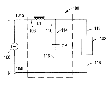
FIG. 2 shows a magnetic ballast circuit 100 for energizing a load 102, such as
a
fluorescent lamp. The ballast 100 has first and second input terminals 104a,b
coupled to an
AC power source 106. In one embodiment, the AC power source 106 provides a 230
Volt,
50 Hz signal to the ballast, such that the first input terminal 104a
corresponds to a so-called
Phase (P) signal and the second input terminal 104b corresponds to a so-called
Neutral (N)
signal.
The ballast further includes an inductive element L 1 having a first terminal
108
coupled to the first input terminal (Phase or P) 104a and a second terminal
110 connected
to a first terminal 112 of the lamp 102. A capacitor CP has a first terminal
114 coupled to
the first lamp terminal 112 and a second terminal 116 coupled to a second lamp
terminal
118, such that the capacitor CP and the lamp 102 are connected in parallel.
The second
lamp terminal 118 and the second capacitor terminal 116 are coupled to the
second input
terminal (Neutral or N) 104b.
As shown in FIG. 3, an adaptor circuit 120 can be coupled between the magnetic
ballast and the lamp 102 to provide a relatively high frequency AC signal to
the lamp for
more efficient operation. Exemplary adaptor circuits are disclosed in co-
pending and
commonly assigned U.S. Patent Application No. 08/753,044, and U.S. Patent No.
4,682,083 (Alley), which are incorporated herein by reference.
In operation, current flowing through the first inductive element L1 and the
parallel
capacitor CP resonates in series at a characteristic resonant frequency which
is determined
by the impedance values of the first inductive element L 1, the parallel
capacitor CP, and the
lamp 102. The series resonance provides a voltage level which is greater than
that of the
-5-
CA 02346938 2001-04-11
WO 00/22892 PCT/US99/22378
input line voltage for increasing the power available to the lamp 102. In an
exemplary
embodiment, the impedance values of the first inductor L1 and the parallel
capacitor CP are
selected for series resonance at about 50 Hertz. Illustrative impedance values
for the first
inductor L 1 and the parallel capacitor CP are 1.5 Henrys and 0.33
microfarads, respectively.
In the exemplary embodiment of FIG. 2, the 230 Volt 50 Hertz input signal is
effective to start the lamp without a starter 16 (FIG. 1). In addition, the
power dissipation
is significantly less than that of a conventional ballast 10. For example,
typical values for
the prior art ballast of FIG. 1 are 1.5 Henrys for the inductor L and 3.0
microfarads for the
capacitor C. In contrast, illustrative values for the components in the
ballast of FIG. 2
1o include 1.5 Henrys for the first inductor L1 and 0.33 microfarads for the
parallel capacitor
CP. The lower capacitance of capacitor CP, as compared with capacitor C,
provides a
power reduction of about one order of magnitude over the prior art ballast of
FIG. 1.
FIG. 4 shows a ballast circuit 200 which provides a user-selectable power
level to
a lamp 202. That is, the ballast 200 has a dimming feature which allows the
intensity of
light emitted by the lamp 202 to be controlled. The ballast includes a first
inductive element
L1 coupled to the lamp 202 and a plurality of capacitors CPa-n coupled in
parallel with the
lamp. Coupled in series with each of the capacitors CPa-n is a respective
switch SWa-n.
The position of each of the switches SW, i.e., open or closed, is
independently controlled
by a switch control circuit 204. The control circuit 204 is coupled to a user
interface 206,
such as a dial, which is manually actuable by a user. Alternatively, lamp
light intensity can
be controlled by other user interface devices including timers, voice
recognition systems,
computer control systems or other data input mechanisms known to one of
ordinary skill in
the art.
In operation, the total capacitance provided by the capacitors CP determines
the
amount of power that is delivered to the lamp 202. Where the input signal,
here shown as
corresponding to Phase and Neutral, has a fixed frequency, i.e., 50 Hertz,
maximum power
occurs when the impedance values of the first inductor L1 and the parallel
capacitor CP are
selected to resonate at this frequency. And while the input signal frequency
remains fixed,
altering the total capacitance provided by the capacitors CPa-n alters the
power at the lamp.
-6-
CA 02346938 2001-04-11
WO 00/22892 PCTNS99/22378
As shown in FIG. 5, the voltage VP 208, which corresponds to the voltage
across
the lamp 202 (and each of the parallel capacitors CPa-n), is determined by the
total
impedance of the first inductor L1 and the parallel capacitors CPa-n. At 50
Hertz, which
corresponds to the frequency of the exemplary input signal, particular
impedance values for
the first inductor L1 and the parallel capacitors CPa-n provide a peak voltage
210 for the
voltage VP. It is understood that a predetermined configuration for the
switches SWa-n
provides a total capacitance for the parallel capacitors CPa-n which
corresponds to the peak
VP voltage 210. Since the impedance of the first inductor L1 is fixed in the
illustrated
embodiment, the voltage VP can be set to a predetermined value by selecting
the total
capacitance provided by the parallel capacitors CPa-n. That is, by switching
in certain ones
of the parallel capacitors CPa-n, a desired power level can be provided to the
lamp 202 for
selecting an intensity level for the light emitted by the lamp, i.e., the lamp
can be dimmed.
The user can control the lamp light intensity by actuating the dial 206 which
ultimately
controls the state of the switches SWa-n to provide a desired light intensity.
For example,
at maximum power, each of the switches SWa-n is closed. And to decrease the
light
intensity, i. e. , dimming, some of the switches SW transition to an open
state to alter the total
capacitance provided by the capacitors CPa-n.
FIG. 6 shows another embodiment of a ballast circuit 300 having a dimming
feature.
The ballast includes an inductive element L 1 coupled between an optional
adaptor circuit 302
and a first input terminal 304a. First and second capacitors CP1,CP2 are
coupled end to end
between the first and second input terminals 304a,b. A switching element Q1,
shown here
as a transistor, is coupled to a diode network formed from diodes Dl-4, as
shown.
The switching element Q1 has a first terminal 306 coupled to a point between
the
first and second diodes D1,D2, which are coupled end to end across the second
capacitor
CP2. A second terminal 308 of the switching element Q 1 is coupled to a
control circuit 310
and a third terminal 312 of the switching element is coupled to a point
between the third and
fourth diodes D3,D4, which are also coupled end to end across the second
capacitor CP2.
The control circuit 310 is effective to control the conduction state of the
switching element
Q1.
CA 02346938 2001-04-11
WO 00/22892 PCT/US99/22378
In operation, the input signal, a 230 volt 50 Hertz signal for example, is
received at
the first and second input terminals 304a,b and energizes the circuit elements
including the
lamp 314 which emits visible light. The control circuit 310 controls the
conduction state of
the switching element Q1 via a control signal 316 so as to provide a desired
intensity level
for the light. Light intensity is controlled by altering the total capacitance
provided by the
first and second capacitors CP1,CP2. When the switching element Q1 is
conductive or ON,
the second capacitor CP2 is effectively shorted so that impedance provided by
the second
capacitor is removed from the circuit. And when the switching element is non-
conductive
or OFF, the total capacitance includes the capacitance of the second capacitor
CP2. In one
embodiment, maximum power, i.e., highest lamp light intensity, occurs when the
switching
element is ON.
The control circuit 310 monitors the voltage to the lamp 314 via feedback
signals
318a,b,c, which monitor the input signal and load voltage, and maintains a
predetermined
lamp power level by controlling the conduction state of the switching element
Q1. The
control circuit 310 controls the duty cycle of the switching element Q 1 which
determines the
total capacitance provided by the first and second capacitors CP1,CP2. It is
understood that
the frequency of the control signal 316 need only be greater than the
frequency of the input
signal and can be orders of magnitude greater.
In other embodiments, further switching elements and control circuits can
control
2o further capacitors. For example, a plurality of capacitors of varying
impedance can be
coupled in the circuit for added resolution of the load voltage.
FIG. 7 shows an alternative embodiment 300' of the ballast circuit 300 of FIG.
6,
wherein like reference designations indicate like elements. The ballast
circuit 300' includes
a triac TR1 coupled to a point between the first and second capacitors
CP1,CP2. The triac
TRl is coupled to a control circuit 310' which controls the conduction state
of the triac. The
conduction state of the triac TRldetermines the total capacitance provided by
the first and
second capacitors CP1,CP2. The control circuit 310' is effective to provide a
selected lamp
light intensity and/or a desired load voltage level.
In FIG. 8, a ballast circuit 300" includes first and second capacitors CP1,CP2
each
3o coupled in parallel with the lamp 314. A triac TR1 is coupled in series
with the first
_g_
CA 02346938 2001-04-11
WO 00/22892 PCT/US99/22378
capacitor CPl for controlling whether the impedance associated with the first
capacitor is
present in the circuit. That is, when the triac TR1 is conductive the
impedance of the first
capacitor CP1 forms a part of the total capacitance provided by the first and
second
capacitors CPl,CP2. The control circuit 310" controls the conduction state of
the triac TRl
so as to provide a selected level of light intensity and/or load voltage.
FIG. 9 shows a ballast circuit 400 having a first inductive element L1 coupled
to a
lamp 402. A first capacitor CP1 and a first winding 404a of a transformer 404
are coupled
in series such that the series-coupled first capacitor CP1 and first winding
404a are coupled
in parallel with the lamp 402. A second winding 404b of the transformer is
coupled to a
control circuit 406.
In operation, the control circuit 406 controls the impedance of the first
winding 404a
of the transformer. That is, the control circuit 406 provides a signal to the
second winding
404b that is effective to cancel a selected amount of flux generated by the
first winding 404a
of the transformer. When the flux is completely canceled, the first winding
404a provides
a small DC resistance to the circuit. The control circuit 406 can provide a
signal to the
second winding 404b that cancels a predetermined portion of the flux generated
by the first
winding. The amount of flux that is canceled can vary from substantially all
to substantially
none. Thus, the control circuit 406 provides a selected impedance for the
first winding 404a
so as to select a desired power to the lamp 402 by controlling the resonant
characteristics of
2o the circuit. In one embodiment where the AC input signal has a
predetermined amplitude
and frequency, 230 volts at 50 Hertz for example, the power to the lamp 402 is
readily
controlled by selecting a desired impedance value for the first winding 404a
by canceling a
desired amount of flux.
FIG. 10 shows an exemplary embodiment of a ballast circuit 500 including a
first
inductive element L1 and a parallel capacitor CP coupled to a lamp 502. A
first transformer
504 includes a first winding LT1 coupled between a first input terminal 506a
and the first
inductive element L1 and a second winding LT2 coupled to a signal generator
508. A
detection circuit 510 includes first, second, and third inductive detection
elements
LD1,LD2,LD3, which are inductively coupled, and a signal detector 512. The
first and
-9-
CA 02346938 2001-04-11
WO 00/22892 PCTNS99/22378
second detection elements LD1,LD2 are coupled to opposite ends of the lamp 502
and the
third detection element LD3 is coupled to a signal detector 512.
In operation, an input signal having a given amplitude and frequency, 230
volts and
50 Hertz for example, is provided to the input terminals 506a,b of the
circuit. The signal
generator 508, under the control of a user, impresses a data signal having a
predetermined
amplitude and frequency upon the second transformer winding LT2 which induces
a
corresponding voltage on the first transformer winding LT 1. The data signal
propagates to
the circuit elements which generates a series resonance between the first
inductive element
L1 and the parallel capacitor CP. This resonant signal generates a
corresponding signal that
1o induces a voltage on the third detection element LD3 which corresponds to a
flux differential
between the first and second detection elements LDl,LD2. The voltage appearing
on the
third detection element LD3 is detected by the signal detector 512.
FIG. 11 shows a ballast circuit having an electronic adapter circuit 514 which
includes the detection circuit 510 of FIG. 10. The detection circuit 510 is
coupled to a load
power control circuit 516 for controlling the power delivered to the lamp 502
based upon
the information provided by the signal detector 512. Thus, a user can vary the
light
intensity of the lamp by controlling the signal introduced to the circuit by
the signal
generator 508.
It is understood that the characteristics of the data signal produced by the
signal
generator 508 can vary widely, provided that the signal appears on the
transformer first
winding LT 1. An exemplary data signal has a frequency of about 1 k Hertz and
an amplitude
of about 1 volt. The data signal can also be modulated, such as by frequency-
shift keying
for example. It is further understood that the data signal can be provided in
pulses of
various durations for detection by the detection circuit.
Providing a data signal by means of introducing a relatively low frequency
series
current into the circuit is to be contrasted with conventional circuits that
generate a relatively
high frequency signal across the input terminals of the circuit. Such high
frequency signals
dissipate relatively quickly and may conflict with FCC regulations.
-10-
CA 02346938 2001-04-11
WO 00/22892 PCT/US99/Z2378
It is understood that the series power line communication circuit disclosed
herein is
not limited to dimming ballast circuits, but rather has a wide range of
applications where it
is desirable to send information from one location in a circuit to another.
One skilled in the art will appreciate further features and advantages of the
invention
based on the above-described embodiments. Accordingly, the invention is not to
be limited
by what has been particularly shown and described, except as indicated by the
appended
claims. All publications and references cited herein are expressly
incorporated herein by
reference in their entirety.
What is claimed is:
-11-