Note: Descriptions are shown in the official language in which they were submitted.
CA 02346945 2001-04-11
wo oonsio6 pcTnrs~naz6~
POLYCRYSTALLINE DIAMOND MEMBER
AND METHOD OF MAKING THE SAME
BACKGROUND
The invention pertains to a polycrystalline
diamond member, and in particular, to a polycrystalline
diamond member having a backing of polycrystalline
diamond and a layer of a hard chemical vapor deposition
(CVD) coating, i.e., a hard material applied by CVD
techniques, on the backing.
Heretofore, a typical polycrystalline diamond
compact comprises a backing of tungsten carbide (or
cobalt cemented tungsten carbide) and a polycrystalline
diamond layer on the backing. The polycrystalline
diamond layer comprises diamond particles bridged
together (i.e., bonded together by bridging) with a
catalyst (e.g., cobalt) at the interstices of the
diamond particles. The cobalt acts as a catalyst for
the bridging together of the diamond particles. Such a
polycrystalline diamond compact is shown and described
in U.S. Patent No. 4,604,106 to Hall et al. for a
COMPOSITE POLYCRYSTALLINE DIAMOND COMPACT, wherein the
Hall et al. patent is hereby incorporated by reference
herein. Although it depends upon the specific
application for use, in the case of use as a
polycrystalline diamond (PCD) blank for a PCD cutting
insert, these polycrystalline diamond compacts are cut
into sections and then polished to some extent to form
a PCD blank whereby the PCD blank is then brazed into a
pocket in a substrate for the PCD cutting insert.
CA 02346945 2001-04-11
WO 00!28106 PCT/US99I24267
-2- -
The PCD blank has a rake surface and flank surfaces
which intersect to define the cutting edges of the PCD
cutting insert. The typical PCD blank has a catalyst
(e. g., cobalt) content between about 5 weight percent
and about 6 weight percent and the average particle
size of the diamond particles varies depending upon the
application. The broader range for the average
particle size of the diamond particles may be between
about 2 micrometers (gym) and about 25 ~,m with other
ranges of between about 2 ~Cm and about 10 ~.m and
between about l0 ~,m and about 25 Vim.
In a co-pending United States patent
application by E.J. Oles and L. E. Thomas entitled
CUTTING INSERT WITH IMPROVED FLANK SURFACE ROUGHNESS
AND METHOD OF MAKING, which is hereby incorporated by
reference herein, and assigned to the assignee
(Kennametal Inc. of Latrobe, Pennsylvania 15650, USA)
of this patent application, there is disclosed a PCD
cutting insert which includes a PCD blank. The PCD
blank has a rake surface that has been roughened using
ion milling, laser or plasma etching so as to achieve a
surface roughness sufficient to provide for microscopic
chip control during a material removal process. The
PCD blank has been finish-ground so that on the flank
surfaces there are the finish-grind lines therein which
lie in a direction that is generally parallel to the
cutting edges, and the flank surfaces have been
polished so that they have a mirror finish (less than
5 microinches, Ra). Such a PCD cutting insert provides
for microscopic chip control due to the roughened rake
surface and also provides a workpiece surface_finish
that approaches theoretical values due to the
smoothness of the flank~surfaces.
While the above-described earlier PCD cutting
insert provides certain advantages and it is a very
satisfactory PCD cutting insert, certain aspects for
improvement still remain.
CA 02346945 2001-04-11
WO 00/28106 PCTNS99l24267
_3_
In the above-described earlier PCD cutting
insert, the surface which contacts the workpiece during
the material removal process is not especially made for
contacting the workpiece surface. In other words, the
microstructure of the diamond layer of the earlier PCD
blank is generally consistent throughout. It would be
highly desirable to provide a PCD cutting insert that
has a PCD blank with a surface which contacts the
workpiece that has been especially made to accommodate
such contact, and wherein the PCD blank also provides
for microscopic chip control and a workpiece surface
finish that approaches theoretical values.
In the above-described earlier PCD cutting
insert, the rake surface achieves its roughness through
a separate roughening step such as ion milling, plasma
etching or laser blading. It would be highly desirable
to provide a PCD cutting insert with a PCD blank with a
roughened rake surface wherein the roughness is not
formed by a separate processing step, and wherein the
PCD blank also provides for microscopic chip control
and a workpiece surface finish that approaches
theoretical values.
SUMMARY
In one form thereof, the invention is a
polycrystalline diamond member which includes a
backing, and a layer of polycrystalline diamond on the
backing wherein the layer of polycrystalline diamond
has a rake surface and a flank surface. The layer of
polycrystalline diamond has an interior region adjacent
to the backing and an exterior region adjacent to the
interior region wherein the exterior region terminates
at the rake surface. The interior region comprises
interior diamond particles and a catalyst wherein the
interior diamond particles are bridged together so as
to form interstices therebetween, and the catalyst is
at the interstices of the interior diamond particles.
CA 02346945 2001-04-11
WO 00/28106 PCTNS99/24267
-4-
The exterior region comprises exterior diamond
particles bridged together so as to form interstices
therebetween and the exterior region is essentially
free of the catalyst. A chemical vapor deposition-
s applied hard material essentially surrounds the
exterior diamond particles.
In another form thereof, the invention is a
polycrystalline diamond cutting insert which comprises
a substrate that contains a pocket therein. A
polycrystalline diamond blank has a backing and a layer
of polycrystalline diamond on the backing. The layer
of polycrystalline diamond has an interior region
adjacent to the backing and an exterior region adjacent
to the interior region. The interior region comprises
interior diamond particles and a catalyst wherein the
interior diamond particles are bridged.together so as
to form interstices therebetween. The catalyst is at
the interstices of the interior diamond particles. The
exterior region comprises exterior diamond particles
bridged together so as to form interstices therebetween
and the exterior region is essentially free of the
catalyst. A chemical vapor deposition-applied hard
material essentially surrounds the exterior diamond
particles.
In still another form thereof, the invention
is a method of making a polycrystalline diamond member
comprising the steps of: providing a backing;
providing a polycrystalline diamond layer on the
backing wherein the polycrystalline diamond comprises a
plurality of diamond particles and a catalyst with the
diamond particles being bridged together so as to form
interstices therebetween and the catalyst being at the
interstices of the diamond particles; removing the
catalyst from the polycrystalline diamond layer
beginning at a portion of the surface of the
polycrystalline diamond layer to a predetermined depth
so as to form: an exterior region comprising exterior
CA 02346945 2001-04-11
WO 00/28106 PCTNS99/24Z67
_5_
ones of the diamond particles bridged together so as to
form interstices therebetween, and the exterior region
being essentially free of the catalyst, and an interior
region inwardly of the exterior region, and the
interior region comprising interior ones of the diamond
particles and a catalyst, and the interior diamond
particles being bridged together so as to form
interstices therebetween, and the catalyst being at the
interstices of the interior diamond particles; and
depositing beginning at the portion of the surface of
the polycrystalline diamond layer a volume of hard
material whereby the rate of deposition is sufficiently
slow so as to permit the hard material to infiltrate
between the bridged-together exterior diamond particles
so as to essentially surround the exterior diamond
particles whereby the exterior region comprises
exterior diamond particles bridged together with the
hard material essentially surrounding the exterior
diamond particles.
In yet another form thereof, the invention is
a method of making a polycrystalline diamond cutting
insert comprising the steps of: providing a substrate
having a pocket therein; providing a polycrystalline
diamond blank having a backing with a polycrystalline
diamond layer on the backing wherein the
polycrystalline diamond layer has a rake surface and a
flank surface which intersect to form a cutting edge,
and the polycrystalline diamond layer comprises a
plurality of diamond particles and a catalyst with the
diamond particles being bridged together so as to form
interstices therebetween and the catalyst being at the
interstices between the diamond particles; removing the
catalyst from the polycrystalline diamond layer
beginning at a portion of the surface of the
polycrystalline diamond layer to a predetermined depth
so as to form: an exterior region comprising exterior
ones of the diamond particles bridged together so as to
CA 02346945 2001-04-11
WO 00/28106 PCT/US99/24267
-6- -
form interstices therebetween, and the exterior region
being essentially free of the catalyst, and an interior
region inwardly of the exterior region and the interior
region comprising interior ones of the diamond
particles being bridged together so as to from
interstices therebetween and the catalyst, and the
catalyst being at the interstices between the interior
diamond particles; depositing beginning at the portion
of the surface of the polycrystalline diamond layer a
volume of hard material whereby the rate of deposition
is sufficiently slow so as to permit the hard material
to infiltrate between the bridged-together exterior
diamond particles whereby the exterior region comprises
the exterior diamond particles bridged together with
the hard material essentially surrounding the exterior
diamond particles; brazing the polycrystalline blank
into the pocket; and finish-grinding the flank surface
of the polycrystalline diamond layer so that the
finish-grind lines lie in a direction generally
parallel to the cutting edge.
BRIEF DESCRIPTION OF THE DRAWINGS
The following is a brief description of the
drawings which form a part of this patent application:
FIG. 1 is an isometric view of a conventional
PCD blank used in connection with a PCD cutting insert
wherein the PCD blank has a backing and a layer of
polycrystalline diamond thereon;
FIG. 2 is a cross-sectional schematic view of
a part of the microstructure of the PCD blank of FIG. 1
taken along section 2-2 of FIG. 1 wherein the PCD blank
has a backing and a polycrystalline diamond layer on
the backing wherein the-polycrystalline diamond layer
comprises diamond particles bridged together and a
catalyst (i.e., cobalt) at the interstices between the
diamond particles;
CA 02346945 2001-04-11
WO 00/28106 PG"T/US99/24267
- ..
FIG. 3 is a cross-sectional schematic view of
the PCD blank like that of FIG. 2, but where a layer of
the catalyst (i.e., cobalt) has been removed from only
the rake surface of the polycrystalline diamond layer
so as to create a region which is essentially free of
the catalyst (i.e., cobalt) and in which the diamond
particles are bridged together;
FIG. 4 is a cross-sectional schematic view of
the PCD blank like that of FIG. 3, but where a layer of
CVD diamond has been deposited on the rake surface of
the polycrystalline diamond layer so as to infiltrate
between (and mechanically adhere to) the diamond
particles in the region which is essentially free of
the catalyst (i.e., cobalt);
FIG. 5 is an isometric view of a PCD cutting
insert wherein the PCD cutting insert has a substrate
with a pocket that receives the PCD blank of FIG. 4;
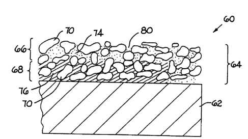
FIG. 6 is a cross-sectional schematic view of
a portion of a PCD blank like that of FIG. 2, but where
a layer of the catalyst (i.e., cobalt) has been removed
from the rake surface and the flank surface of the
polycrystalline diamond layer so as to create a region
which is essentially free of the catalyst (i.e.,
cobalt) and in which the diamond particles are bridged
together; and
FIG. 7 is a cross-sectional view of a PCD
blank like that of FIG. 6, but where a layer of diamond
has been deposited on the rake surface and the flank
surface of the polycrystalline diamond layer so as to
infiltrate between (and mechanically adhere to) the
diamond crystals in the region which is essentially
free of the catalyst (i . a . , cobalt) .
DETAILED DESCRIPTION
The present invention pertains to a
polycrystalline diamond member including a PCD blank
for a cutting insert, a PCD cutting insert utilizing a
CA 02346945 2001-04-11
WO 00/28106 PCT/US99~24267
_g_ _.
PCD blank, a wire die, a wear surface, wear members for
rock cutting equipment, and wear members for drilling
equipment. Broadly speaking and as will become
apparent from the description hereinafter, the
polycrystalline diamond member has a backing on which
there is a polycrystalline diamond layer. The
polycrystalline diamond layer has an exterior region
which comprises diamond particles (i.e., exterior
diamond particles) bridged together (i.e., bonded
together by bridging) with a hard material (e. g.,
diamond) applied by CVD surrounding (and mechanically
adhering to) the exterior diamond particles so there
are no voids in the exterior region. The
polycrystalline diamond layer also has an interior
region between the backing and the exterior region
wherein the interior region includes diamond particles
(i.e., interior diamond particles) bridged together
with a metallic catalyst (e.g., cobalt) at the
interstices of the diamond particles.
Broadly speaking and as will become a
pparent
from the description hereinafter, the process of making
the polycrystalline diamond member comprises the steps
of: (1) providing a PCD blank with a backing and a
polycrystalline diamond layer on the backing wherein
the polycrystalline diamond comprises a plurality of
diamond particles bridged together and the catalyst at
the interstices of the diamond particles; (2) removing
the catalyst from the polycrystalline diamond surface
beginning at one or more selected portions of the
surface of the polycrystalline diamond layer to a
predetermined depth so as to form: (a) an exterior
region comprising the diamond particles (i.e., exterior
diamond particles) bridged together and being
essentially free of the catalyst (i.e., cobalt), and
(b) an interior region inwardly of the exterior region
and the interior region comprising the diamond
particles (i.e., interior diamond particles) and the
CA 02346945 2001-04-11
WO 00/28106 PCT/US99/24267
_9_
catalyst with the interior diamond particles being
bridged together and the catalyst at the interstices of
the diamond particles; and (3) depositing via CVD
techniques beginning at the portion of the surface of
the polycrystalline diamond layer a volume of a hard
material (e. g., diamond) whereby the rate of deposition
is sufficiently slow so as to permit the CVD hard
material to infiltrate between (and mechanically adhere
to) the bridged-together diamond particles in the
exterior region whereby the exterior region comprises
exterior diamond particles bridged together with the
hard material surrounding the bridged-together diamond
particles.
Referring to FIGS. 1 and 2 there is shown a
conventional polycrystalline (PCD) blank generally
designated as 10 and being of a generally triangular
geometry. PCD blank 10 includes a backing layer 12
which preferably comprises a tungsten carbide-cobalt
material. Applicant contemplates that other suitable
material may comprise the backing layer 12. PCD
blank 10 further comprises a polycrystalline diamond
layer 14 which comprises a plurality of diamond crystals
(or particles) 20 (see FIG. 2) bridged together so as to
form interstices therebetween and having a catalyst
material 26 filling (or being at) the interstices of the
diamond crystals 20. The preferred catalyst material 26
is cobalt, but applicant contemplates that other
suitable materials are within the scope of the
invention.
As illustrated by FIG. 2, the catalyst 26
extends to the rake surface 30 of the diamond_layer 14.
The PCD blank 10 also presents flank surfaces 32. The
rake surface 30 and the flank surfaces 32 intersect to
form cutting edges 34 at the juncture thereof. It
should be appreciated that the PCD blank l0 may be made
by conventional methods such as, for example, by those
CA 02346945 2001-04-11
WO 00/28106 PCT/US99/24267
-10- -
disclosed in U.S. Patent No. 4,604,106 to Hall et al.,
which is hereby incorporated by reference herein.
Referring to FIG. 3, after providing the PCD
blank 10, the next step in the process is to remove
essentially all of the catalyst material 26 from the
regions) of the polycrystalline diamond layer 14 near
one or more selected portions of the surface. The
result of the removal step is to form in the
polycrystalline diamond layer 14 an exterior region 16
and an interior region 18, which are described in more
detail hereinafter, wherein these regions have
different microstructures.
In the specific embodiment shown in FIG. 3,
the catalyst 26 is removed from only the rake
surface 30 of the polycrystalline diamond layer 14 and
the catalyst 26 is not directly removed from the flank
surface 32. However, even though the catalyst is not
directly removed from the flank surface 32, the
exterior region 16 extends to the flank surface 32 near
the point where the rake surface 30 and the flank
surface 32 intersect to form the cutting edge 34.
The actual process to accomplish this removal
may be an electrochemical process or an acid treatment.
As an example of an acid treatment, the blank may be
dipped in a solution of one part HN03 and three parts
water at 40°C for about 15 minutes. This process
(i.e., acid treatment) or an electrochemical process
would result in an essentially catalyst-free surface.
The electrochemical process is preferred since such a
process would be self-arresting due to the fact that
the diamond remaining after the removal of the metallic
catalyst (e. g., cobalt) is an insulator.
Still referring to FIG. 3, it can be seen
that the removal of the catalyst 26 from the rake
surface 30 has created an exterior region 16 in which
there is essentially no catalyst (cobalt) but only the
diamond particles 20 (or exterior diamond particles)
CA 02346945 2001-04-11
WO 00/28106 PCT/US99/24Z67
-I1-
bridged together (i.e., bonded together by bridging).
The removal of the catalyst 26 has also created an
interior region 18 which still contains catalyst 26
surrounding the bridged-together diamond particles 20
(or interior diamond particles). The interior
region 18 extends to the flank surface 32.
Referring to FIG. 4, the next step in the
process is to apply via a CVD process a diamond coating
to the rake surface 30 of the PCD blank 10 illustrated
in FIG. 3. The deposition rate of the diamond material
should be slow enough so that the diamond material
infiltrates the catalyst-free exterior region and
surrounds the diamond particles so that there are
essentially no voids in the exterior region comprising
the diamond particles and diamond material. It is
preferable that the diamond material also mechanically
adheres to the diamond particles. The above-described
degree of infiltration and mechanical adherence should
occur if the deposition rate is less than about one
micron per hour, and more preferably less than about
0.5 microns per hour. The infiltration is also
enhanced if the particle size of the diamond material
is small enough so that the diamond particles easily
move into the interstices between the exterior diamond
particles. In this regard, one preferred average
particle size for these diamond particles is between
about 10 um and 15 ~Cm.
Referring to the deposition techniques,
although a number of deposition techniques may be
acceptable, acceptable deposition techniques are
generally described and disclosed in U.S. Patent
No. 5,482,748 to Soderberg et al, for a METHOD FOR
DIAMOND COATING BY MICROWAVE PLASMA (which is hereby
incorporated by reference herein), the article by
Haubner et al. entitled "Diamond growth by hot-filament
chemical vapor deposition: state of the art," Diamond
and Related Materials, 2 (1993), pages 1277-1294 (which
CA 02346945 2001-04-11
WO 00128106 PCT/US99/24I67
-12- ..
is hereby incorporated by reference herein) provided
that the deposition rate is sufficiently slow to
achieve adequate infiltration as described above. The
result of the diamond deposition step is that the
exterior region 16 comprises the diamond particles 20
bridged together and having the CVD diamond material 24
surrounding the diamond particles 20, as well as
mechanically adhering to.the diamond particles 20.
Stilt referring to FIG. 4, the diamond
l0 particles 20 near the rake surface 30 of the
polycrystalline diamond layer 14 protrude slightly from
the rake surface so as to create a surface roughness.
This surface roughness is on the order of greater than
microinches, Ra, and more preferably, on the order
15 of greater than 30 microinches, Ra. To some extent the
diamond crystals protrude from the flank surface 32 at
the point near the intersection of the rake surface 30
and the flank surface 32. However, as will be
described hereinafter, once the PCD blank has been
affixed to the PCD cutting insert, the flank
surfaces 32 may be finish-ground and polished so as to
remove any surface roughness caused by the protrusion
of the diamond particles.
FIG. 5 illustrates a PCD cutting insert
generally designated as 40 having the generally
triangular PCD blank 10 made according to the above
process. The PCD cutting insert 40 has a substrate 42
which contains a pocket 44. The PCD blank 10 is
affixed (e.g., brazed) into the pocket 44. The PCD
blank 10 has a polycrystalline diamond layer 14 with a
rake surface 30. The diamond layer 14 is on the top
surface of a the backing 12. The diamond layer 14 also
presents flank surfaces 32 which intersect with the
rake surface 30 to form cutting edges 34.
After the PCD blank 10 has been brazed into
the pocket 44, each flank surface 32 thereof may be
finish-ground so that the finish-grind lines 46 are
CA 02346945 2001-04-11
WO 00/28106 PC"TNS99/14267
-13- w
generally parallel to the direction of its
corresponding cutting edges 34. Each flank surface 32
is then polished so as to attain a surface roughness of
less than five microinches, Ra. The rake surface 30 of
the polycrystalline diamond layer 14 has a CVD layer
from the exterior region of the diamond layer
protruding therefrom so as to create a surface
roughness sufficient to achieve microscopic chip
control.
Because the exterior region 16 of the
polycrystalline diamond layer 14 comprises diamond
particles and a CVD diamond coating surrounding the
diamond particles, the exterior region, and hence, the
surface of the exterior region 16 of the
polycrystalline diamond layer 14, is especially suited
for contacting the workpiece surface. .The portions of
the polycrystalline diamond layer 14 which have the
diamond particles in the diamond material 24 are the
rake surface 30 and a portion of the flank surface 32
in the vicinity of the intersection of the rake
surface 30 and the flank surface 32, i.e., the cutting
edge 34.
It can thus be appreciated that the PCD
cutting insert 40 will provide a PCD blank 10 with a
rake surface 30 wherein the roughness provides for
microscopic chip control and a flank surface 32 which
has a surface finish that provides for a workpiece
surface finish that approaches theoretical values. It
can also be appreciated that the PCD cutting insert 40
will provide a PCD blank 10 wherein the rake surface 30
and the portion of the flank surface 32 adjacent to the
cutting edge 34 (which includes the cutting edge 34) is
especially suited for contacting the workpiece during a
material removal operation.
The specific embodiment illustrated in
FIGS. 3 and 4 occurred as a result of the removal of
the cobalt catalyst from only the rake surface of the
CA 02346945 2001-04-11
WO 00/28106 PCTNS99/24Z6~
-14- w
PCD blank. In another embodiment, the catalyst
(cobalt) may be removed from both the rake surface and
the flank surface of the PCD blank.
In this regard and referring to FIGS. 6 and
7, there is illustrated in FIG. 6 a cross-section of
the PCD blank 60 which has had the catalyst (i.e.,
cobalt) removed from the portions of the
polycrystalline diamond layer 64 near the rake
surface 80 and the flank surface 82. Thus, it can be
seen that there is a portion of the exterior region 66
which extends along the entire rake surface and another
portion of the exterior region 66 which extend along
the entire flank surface 82. These exterior regions 66
are essentially cobalt (or catalyst)-free and comprise
particles of diamond bridged together. The interior
region 68 is contained between the exterior region 66
and the surface of the backing 62. The interior
region 68 does not extend to the rake surface 80 or the
flank surface 82.
FIG. 7 shows the cross-section of the PCD
blank 60 of FIG. 6 wherein a diamond layer 74 has been
applied to the flank surface 82 and the rake
surface 80. The diamond layer 74 is initially applied
at a rate of less than about one micron per hour (and
more preferably at a rate of less than about
0.5 microns per hour) so that the diamond material 74
infiltrates between (and mechanically adheres to) the
diamond particles 20 so as to create an exterior
region 66 which extends inwardly from the rake
surface 80 and from the flank surface 82.
In a fashion like that of FIG. 4, the diamond
particles 70 protrude from the rake surface 80 and the
flank surface 82. The rake surface 80 thus has a
surface roughness on the order of greater than
15 microinches, Ra, and more preferably, on the order
of greater than 30 microinches, Ra. The diamond
particles 70 that protrude from the flank surface 82;
CA 02346945 2001-04-11
wo oonaio6 Pcrn~s~naz6~
-15-
however, as will be described hereinafter, the flank
surface may be finish-ground and polished so as to
remove any surface roughness caused by the protrusion
of the diamond particles 70.
Like for the embodiment of FIG. 4, the PCD
blank is brazed into a pocket of the substrate of a PCD
cutting insert. The flank surface 82 of the PCD
blank 60 is finish-ground, and then polished to achieve
a surface roughness of less than 5 microinches, Ra,
which provides for a workpiece surface finish that
approaches the theoretical value. The rake surface 80
has a surface roughness sufficient to provide
microscopic chip control. Hence, it is seen that the
PCD cutting insert which uses the PCD blank formed from
the PCD blank like FIG. 7 provides for microscopic chip
control and a workpiece surface finish approaching
theoretical value.
The above discussion has had a focus on the
CVD application of a diamond material to the exterior
region after the removal of the catalyst therefrom.
However, it should be appreciated that other hard
materials may be applied to the exterior region after
the removal of the catalyst from the cutting insert.
In this regard, these hard materials may
include titanium carbonitride which is applied by
moderate temperature chemical vapor deposition (MTCVD)
techniques. The deposition temperature for the MTCVD
process is about a temperature of 850°C.
These hard materials may also include at
least one of alumina, titanium nitride, titanium
carbonitride or titanium carbide which is applied by
plasma assisted chemical vapor deposition (PACVD).
The deposition temperature for the PACVD process ranges
between about 600°C and about 700°C.
The patents and other documents identified
herein are hereby incorporated by reference herein.
CA 02346945 2001-04-11
WO OO1Z8106 PGT/US99lZ4267
-16-
Other embodiments of the invention will be
apparent to those skilled in the art from a
consideration of the specification or practice of the
invention disclosed herein. It is intended that the
specification and examples be considered as
illustrative only, with the true scope and spirit of
the invention being indicated by the following claims.