Note: Descriptions are shown in the official language in which they were submitted.
CA 02347551 2001-05-15
Specification
SEMICONDUCTOR LASER APPARATUS
Background of the Invention
The present invention relates to a semiconductor laser apparatus,
semiconductor laser module, optical transmitter and wavelength
division multiplexing communication system, all of which are used in
the optical communication system.
In recent years, various new techniques have been developed in
the field of semiconductor laser used in the optical communication
system. For example, in the wavelength division multiplexing (WDM)
communication system, a single-mode laser (e.g., distributed feedback
(DFB) laser) has usually been used as a source of signal light. In a
dense WDM system (DWDM system), however, a crosstalk between
channels may occur to deteriorate signals when the lasing wavelength
of the signal light source is out of a predetermined level. To avoid such
a problem, a technique of regulating the wavelength of the laser beam
launched from a light-emitting device has been developed.
For example, there has been proposed a semiconductor laser
apparatus which comprises a light-emitting device for outputting a
laser beam and a wavelength monitoring portion for sensing the
wavelength of the laser beam outputted from the light-emitting device
and which can control the light-emitting device relating to its
temperature based on the wavelength of the laser beam sensed by the
wavelength monitoring portion so as to control the wavelength of the
laser beam launched from the light-emitting device.
z
CA 02347551 2001-05-15
Summary of the Invention
A semiconductor laser apparatus of tl~e present invention
comprises a light-emitting portion including a light-emitting device for
outputting a laser beam, a light-receiving element for receiving the
laser beam outputted from said light-emitting device, a wavelength
monitoring portion including an optical system disposed between said
light-emitting device and said light--receiving element, a control portion
for controlling the wavelength of the laser beam outputted from said
light-emitting device by controlling the temperature of said
light-emitting device based on the wavelength of the laser beam
detected by said wavelength monitoring portion, an optical isolator
disposed on the optical path between said light-emitting device and
said wavelength monitoring portion for preventing the light from
returning from said wavelength monitoring portion back to said
light-emitting device, and a temperature regulating portion for
independently controlling the temperatures of said Light-emitting
portion and wavelength monitoring portion.
A semiconductor laser module of the present invention comprises
a semiconductor laser apparatus having a light-emitting portion
including a light-emitting device for outputting a laser beam, a
light-receiving element for receiving the laser beam outputted from
said light-emitting device, a wavelength monitoring portion including
an optical system disposed between said light-emitting device and said
light-receiving element, a control portion for controlling the
wavelength of the laser beam outputted from said light-emitting device
by controlling the temperature of said light-emitting device based on
the wavelength of the laser beam detected by said wavelength
monitoring portion, an optical isolator disposed on the optical path
between said light-emitting device and said wavelength monitoring
2
CA 02347551 2001-05-15
portion for preventing the light from returning from said wavelength
monitoring portion back to said light-emitting device and a temperature
regulating portion for independently controlling the temperatures of
said light-emitting portion and wavelength monitoring portion, a
package being configured to seal at least the light-emitting portion in
said semiconductor laser apparatus in an air-tight manner, and an
optical fiber being configured to receive and externally transmitting the
laser beam outputted from said semiconductor laser apparatus.
The present invention provides an optical transmitter for
transmitting optical signals in a wavelength division multiplexing
communication system, comprising a semiconductor laser module
having a light-emitting device for outputting a laser beam, a
light-receiving element for receiving the laser beam outputted from
said light-emitting device, a wavelength monitoring portion including
an optical system disposed between said light-emitting device and said
light-receiving element, a control portion for controlling the
wavelength of the laser beam outputted from said light-emitting device
by controlling the temperature of said light-emitting device based on
the wavelength of the laser beam detected by said wavelength
monitoring portion, an optical isolator disposed on the optical path
between said light-emitting device and said wavelength monitoring
portion for preventing the 1 fight from returning from said wavelength
monitoring portion back to said light-emitting device, and a
temperature regulating portion for independently controlling the
temperatures of said light-emitting portion and wavelength monitoring
portion.
The present invention also provides a wavelength division
multiplexing communication system having a plurality of optical
transmitters for transmitting optical signals, a multiplexer for
3
CA 02347551 2001-05-15
wavelength multiplexing mufti-channel optical signals transmitted from
said optical transmitters, a plurality of optical amplifiers connected to
one another in a plurality of stages for amplifying and relaying the
multiplexed optical signal from said multiplexer, a branching filter for
wavelength separating the amplified optical signals from the optical
amplifiers for the respective channels and a plurality of optical
receivers for receiving the respective optical signals separated by the
branching filter, each of said optical transmitters comprising a
semiconductor laser module having a light-emitting portion including a
light-emitting device for outputting a laser beam, a light-receiving
element for receiving the laser beam outputted from said light-emitting
device, a wavelength monitoring portion including an optical system
disposed between said light--emitting device and said light-receiving
element, a control portion for controlling the wavelength of the laser
beam outputted from said light-emitting device by controlling the
temperature of said light-err~itting device based on the wavelength of
the laser beam detected by said wavelength monitoring portion, an
optical isolator disposed on the optical path between said light-emitting
device and said wavelength monitoring portion for preventing the light
from returning from said wavelength monitoring portion back to said
light-emitting device, and a temperature regulating portion for
independently controlling the temperatures of said light-emitting
portion and wavelength monitoring portion.
Brief Description of the Drawings
Fig. 1 is a plan cross-sectional view showing a semiconductor
laser module constructed according to a first embodiment of the present
invention.
Fig. 2 is a plan cross-sectional view showing a semiconductor
4
CA 02347551 2001-05-15
laser module constructed according to a second embodiment of the
present invention.
Fig. 3(A) is a plan cross-sectional view showing a
semiconductor laser module constructed according to a third
embodiment of the present invention while Fig. 3(B) is a side view
thereof showing a PD carrier.
Fig. 4 is a plan cross-sectional view showing a semiconductor
laser module constructed according to a fourth embodiment of the
present invention.
Fig. 5 is a plan cross-sectional view showing a semiconductor
laser module constructed according to a fifth embodiment of the
present invention.
Fig. 6 is a plan cross-sectional view showing a semiconductor
laser module constructed according to a sixth embodiment of the
present invention.
Fig. 7 is a graph illustrating variable wavelength relative to the
current injected into a light-emitting device.
Fig. 8 is a graph illustrating the temperature characteristics of an
optical filter.
Fig. 9 is a graph illustrating the temperature characteristics of an
optical isolator.
Figs. 10(A) and (B) are plan and side views schematically
showing a semiconductor laser module constructed according to a
seventh embodiment of the present invention.
Fig. 11 (A) is a plan view schematically showing a
semiconductor laser module constructed according to an eighth
embodiment of the present invention while Fig. 11(B) is a block
diagram showing the layout of a wavelength monitoring portion.
Fig. 12 is a plan cross-sectional view showing a semiconductor
CA 02347551 2001-05-15
laser module constructed according to a ninth embodiment of the
present invention.
Fig. 13 is a view showing an optical transmitter which is used in
a wavelength division multiplexing communication system constructed
according to a tenth embodiment of the present invention.
Detailed Description
Several embodiments of the present invention will now be
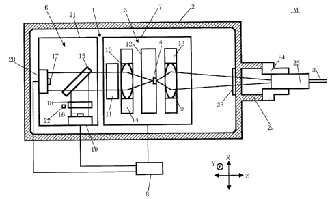
described with reference to the drawings. Fig. 1 is a plan
cross-sectional view showing a semiconductor laser module
constructed according to a first embodiment of the present invention.
Referring to F'ig. 1, the semiconductor laser module M according
to the first embodiment of the present invention comprises a
semiconductor laser apparatus 1 for outputting a laser beam, a package
2 air-tightly sealing the semiconductor laser apparatus 1 and an optical
fiber 3 which receives the laser beam outputted from the semiconductor
laser apparatus 1 and then transmits it externally.
The semiconductor laser apparatus 1 comprises a light-emitting
portion 5 including an light-emitting device 4 formed by a
semiconductor laser diode for outputting a laser beam (e.g., DFB laser
diode device having its lasing wavelength band of l.SSp.m), a
wavelength monitoring portion 6 for sensing the wavelength of the
laser beam outputted from the light-emitting device 4, a first
temperature regulating portion 7 including a plurality of Peltier devices
for controlling the temperature of the light-emitting device 4, and a
control portion 8 for controlling the first temperature regulating portion
7 such that the lasing wavelength of the laser beam outputted from the
light-emitting device 4 will be controlled to a desired wavelength
depending on the output of the wavelength monitoring portion 6.
s
CA 02347551 2001-05-15
The light-emitting portion 5 includes a condensing lens 9 for
condensing the laser beam outputted from the front emitting .end of the
light-emitting device 4 (or the right end thereof as viewed in Fig. I )
and a collimating lens 10 for collimating the laser beam outputted from
the back emitting end of the light-emitting device 4 (or the left end
thereof as viewed in Fig. 1 ). The light-emitting device 4 is fixedly
mounted on an LD carrier 1 a. The condensing lens 9 is held by a first
lens holder 13 while the collimating lens 10 is held by a second lens
holder 14.
On the backside of the collimating lens 10 is provided an optical
isolator 11 for preventing the light from returning from the wavelength
monitoring portion 6 back tc> the light-emitting device 4. The optical
isolator 11 may be any one known in the art which has a combination
of light polarizer and Faraday rotator.
The LD carrier 12, first lens holder 13, second lens holder 14
and optical isolator 11 are fixedly mounted on the first temperature
regulating portion 7 including the Pettier devices. Fig. 9 shows the
temperature characteristics of the optical isolator 11 (or the
relationship between the temperature and the isolation). As will be
apparent from Fig. 9, the temperature of the optical isolator 11 is
controlled by the first temperature regulating portion 7 together with
the light-emitting device 4 such that the prevention of returning light
will be maximized.
In Fig. 9, line PS represents the results of an optical isolator of
such a type that uses one stage consisting of a combination of light
polarizer-Faraday rotator-light polarizer. Line PW represents the
results of an optical isolator of such a type that two stages of such PS
type are connected in series. PSW represents the results of an optical
isolator of such a type that used a combination of light
CA 02347551 2001-05-15
polarizes-Faraday rotator-light polarizes-Faraday rotator-light
polarizes.
The wavelength monitoring portion 6 comprises a half mirror (or
optical branching member) I S for branching the laser beam outputted
from the back end of the light-emitting device 4 and collimated by the
collimating lens 10, a first light-receiving element (or photodiode) 16
for receiving one of the laser beams branched by the half mirror 15, a
second light-receiving element (or photodiode) 17 for receiving the
other of the laser beams branched by the half mirror 15 and an optical
filter 18 disposed between the half mirror I S and the first
light-receiving element 16 for varying the wavelength-to-strength
characteristics of the laser beam.
The first and second light-receiving elements 16, 17 are fixedly
mounted on the first and second PD carriers 19, 20, respectively.
PD currents outputted from the first and second light-receiving
elements 16, 17 are inputted into the control portion 8.
The optical filter 18 may be formed as by an etalon comprising a
silica glass and thin-films formed on the opposite sides thereof. The
optical filter 18 has its wavelength characteristics of transmissivity
depending on temperature. For example, the temperature characteristics
(or the relationships between the wavelength and the PD current at the
respective temperatures) of the optical filter 18 if it is formed by
crystal are shown in Fig. 8. Thus, the wavelength monitoring portion 6
is located on the second temperature regulating portion 21 consisting of
Peltier devices or others and spaced apart from the first temperature
regulating portion 7 such that the temperature thereof can be controlled
independently of the light-emitting portion 5.
The control portion 8 controls the first temperature regulating
portion 7 to control the wavelength of the laser beam outputted from
s
CA 02347551 2001-05-15
the light-emitting device 4, based on the values of PD current inputted
from the first and second light-receiving elements 16, 17.
The wavelength monitoring portion 6 includes a temperature
sensor 22 of thermistor or the like for sensing the temperature thereof.
Based on the temperature sensed by the temperature sensor 22, the
second temperature regulating portion 21 is controlled so that the
wavelength monitoring portion 6 reaches the desired temperature.
The side of the package 2 is formed with a window 23 onto
which the beam passed through the condensing lens 9 enters. The side
of the package 2 also includes a flange portion 2a formed thereon, the
end face of which fixedly supports a metal sleeve 24 through YAG
laser welding.
The tip end of the optical fiber 3 is held by a ferrule 25 which is
in turn fixedly mounted on the interior of the sleeve 24 through YAG
laser welding.
The open top of the package 2 is covered with a closure (not
shown). The periphery of the closure is laser welded to the package 2
to seal the interior of the package 2 air-tightly.
The laser beam outputted from the front end of the light-emitting
device 4 is condensed by the condensing lens 9, the condensed beam
entering the optical fiber 3 held by the ferrule 25 through the window
23 and being then transmitted to outside.
On the other hand, the monitoring laser beam outputted from the
back end of the light-emitting device 4 is collimated by the collimating
lens 10 and then enters the wavelength monitoring portion 6 through
the optical isolator 11.
The laser beam entered the wavelength monitoring portion 6 is
branched by the half mirror 1.5 into a beam portion directed to Z-axis
direction (or direction of transmission) and another beam portion
9
CA 02347551 2001-05-15
directed to X-axis direction (ar direction of reflection) which is
perpendicular to the Z-axis direction. The laser beam portion- directed
to the Z-axis direction is received by the second light-receiving
element 17 while the laser beam portion directed to the X-axis
direction is received by the first light-receiving element 16. The PD
currents outputted from the first and second light-receiving elements
16, 17 are inputted into the control portion 8 which in turn controls the
first temperature regulating portion 7 based on the inputted PD currents
such that the wavelength of t:he laser beam outputted from the
light-emitting device 4 is controlled.
The conventional semiconductor laser systems raised a problem
in that the returning beams from the fiber end, beam sputter, optical
filter in the wavelength monitoring portion are summed to provide an
increased beam returned back to the light-emitting device. Particularly,
with DFB laser, the single longitudinal mode would be disturbed by the
external returning light beam to vary the lasing wavelength and/or to
provide an instability such as longitudinal mode hop or the like.
On the contrary, the semiconductor laser module M according to
the first embodiment of the present invention will not vary the lasing
wavelength of the light-emitting device 4 due to the returning light
beam from the wavelength monitoring portion 6 since the optical
isolator 11 for preventing the returning beam from the wavelength
monitoring portion 6 is disposed between the light-emitting device 4.
This can control the lasing wavelength of the light-emitting device 4
more constantly.
Furthermore, the light-emitting portion 5 and wavelength
monitoring portion 6 can be controlled optimum since their
temperatures are independently controlled. Additionally, the optical
isolator 11 prevents the light beam from returned from the wavelength
to
CA 02347551 2001-05-15
monitoring portion 6 back to the light-emitting device 4. This prevents
the degradation of wavelength characteristic such as longitudinal mode
jump or the like in the light-emitting device 4. Therefore, the
wavelength of the light-emitting device 4 can be controlled more stably.
As a result, the reliability in the semiconductor laser module can be
improved. And yet, the degradation of noise characteristic in the light .
beam outputted from the light-emitting device 4 can be avoided since
the optical isolator 11 prevents any returning light from the wavelength
monitoring portion 6 to the light-emitting device 4.
Fig. 2 is a plan cross-sectional view showing a semiconductor
laser module constructed according to a second embodiment of the
present invention.
Referring to Fig. 2, in the second embodiment, the optical
isolator 11 is located on the wavelength monitoring portion 6 and
disposed in front of the half mirror 15 (on the right side thereof as
viewed in Fig. 2). The other structure and advantages are the same as in
the first embodiment.
According to the second embodiment of the present invention,
the prevention of returning light beam can more be optimized since the
light-emitting device 4 and optical isolator 11 are independently
controlled in temperature. If the wavelength monitoring portion ti and
optical isolator 11 are mounted on the same second temperature
regulating portion 21, the light-emitting portion 5 can be reduced in
dimension. Thermal resistance on the first temperature regulating
portion 7 which includes the light-emitting device 4 as a source of heat
and which must have an increased heat radiation can also be reduced.
Fig. 3 is a plan cross-sectional view showing a semiconductor
laser module constructed according to a third embodiment of the
present invention.
m
CA 02347551 2001-05-15
Referring to Fig. 3, the wavelength monitoring portion 6
according to the third embodiment comprises a prism (or optical
branching member) 25 for branching the laser beam outputted from the
light-emitting device 4 into two beam sections respectively inclined
relative to the optical axis by given angles 81 and 82 which are less
than 90 degrees, a first light-receiving element 16 for receiving one of
the beam sections branched by the prism 26, a second light-receiving
element 17 for receiving the other of the beam sections branched by the
prism 26, an optical filter 18 disposed between the first light-receiving
element 16 and the prism 26 for varying the wavelength-to-strength
characteristic of the laser beam, and a PD carrier (or mount member)
27 for mounting the first and second light-receiving elements 16, 17 on
the same plane (or the same mount plane herein). The other structure
and advantages are the same as in the first embodiment.
The whole prism 26 is coated with AR film for suppressing the
reflection of the laser beam. The angles 81 and 02 of the laser beam
sections branched by the prism 26 are preferably substantially equal to
each other (e.g., between 15 and 45 degrees). This is because the light
receiving positions of the first and second light-receiving elements 16,
17 can more easily be determined.
The mount face 27a of the PD carrier 27 on which the first and
second light-receiving elements 16, 17 are mounted is inclined relative
to the direction of incident laser beam by an angle 03 which exceeds 90
degrees (see Fig. 3(B)). The angle A3 of the inclined mount face is
preferably equal to or larger than 95 degrees for reducing the reflected
returning light beam to provide a good property. If the mount face too
largely inclined relative to t:he direction of incident laser beam, no
sufficient PD current capable of being coupled with the light-receiving
elements 16, 17 will be provided. It is therefore preferred that the
12
CA 02347551 2001-05-15
inclined angle 83 is suppressed at least equal to or smaller than 135
degrees to maintain the degradation of cowling efficiency within 3dB.
It is therefore preferred that the inclined angle 83 of the mount face
27a is between 95 degrees and 135 degrees.
The laser beam sections from the light-emitting portion 5
branched by the prism 26 about the optical axis are thus inclined with
relative to the optical axis by the given angles8l and 82.
One of the laser beam sections branched by the prism 26 enters
the optical filter 18 and then is received by the first light-receiving
element 16 through the optical filter 18. The other laser beam section is
received by the second light-receiving element 17. PD currents
outputted from the first and second light-receiving elements 16, 17 are
inputted into the control portion 8 which in turn controls the first
temperature regulating portion 7 based on the two inputted PD currents
such that the wavelength of the laser beam outputted from the
light-emitting device 4 will be controlled.
According to the third embodiment of the present invention, the
first and second light-receiving elements 16, 17 for receiving the laser
beam sections branched by the prism 26 are mounted on the same
mount face 27 of the PD carrier 27. This reduces the number of parts
and the manufacturing cost.
Since the optical adjustment may only be carried out relating to
the one PD carrier 27, the number of manufacturing steps can be
reduced to shorten the manufacturing time.
Since the laser beam is branched by the prism 26 into two laser
beam sections received by the two light-receiving elements 16, 17 on
the one PD carrier 27, the optical path can be reduced to make the
module more compact and small. At the same time, the condensing
efficiency can be improved for conducting the laser beams into the
13
CA 02347551 2001-05-15
light-receiving elements 16, 17.
Fig. 7 is a graph illustrating variable wavelength relative to the
current injected into a light-emitting device. In this graph, solid line
represents expected values in the third embodiment of the present
invention while one-dot chain line represents actual measurements in a
comparative example of ATC', (Auto Temperature Control). As will be
apparent from Fig. 7, in this embodiment of the present invention, it
will be expected that the lasing wavelength of the light-emitting device
4 can more stably be controlled than the comparative example.
Fig. 4 is a plan cross-sectional view showing a semiconductor
laser module constructed according to a fourth embodiment of the
present invention.
Referring to Fig. 4, in the fourth embodiment, the optical
isolator 11 is located on the wavelength monitoring portion 6 and
disposed in front of the prism 26 (or on the right side thereof as viewed
in Fig. 4). The other components and advantages are the same as in the
third embodiment.
According to the fourth embodiment, the prevention of returning
light beam can more be optimized since the light-emitting device 4 and
optical isolator 11 are independently controlled in temperature. If the
wavelength monitoring portion 6 and optical isolator 11 are mounted
on the same second temperature regulating portion 21, the
light-emitting portion 5 can be reduced in dimension. Thermal load on
the first temperature regulating portion 7 can also be reduced.
Fig. 5 is a plan cross-sectional view showing a semiconductor
laser module constructed according to a fifth embodiment of the
present invention.
Referring to Fig. 5, the fifth embodiment is characterized by that
the wavelength monitoring partion 6 is disposed in front of the
14
CA 02347551 2001-05-15
light-emitting portion 5 (or on the right side thereof as viewed in Fig.
S).
The light-emitting portion 5 comprises a collimating lens 10 for
collimating the laser beam outputted from the front (or right as viewed
in Fig. 5) emission end of the light-emitting device 4, a photodiode 28
for receiving the laser beam outputted from the back (or left as viewed
in Fig. 5) emission end of the light-receiving element 4 and for
monitoring the light output thereof, and an optical isolator 11 for
preventing any returning light beam from the wavelength monitoring
portion 6 back to the light-emitting device 4.
The optical branching, member of the wavelength monitoring
portion 6 consists of a first half mirror (or optical branching member)
15a and a second half mirror (or optical branching member) 15b. These
half mirrors are disposed in series along the Z-axis direction and
spaced apart from each other with a given spacing.
The first half mirror 1. 5a divides the laser beam outputted from
the light-emitting device 4 into two beam sections, a beam section in
the first direction (or X-axis direction) on the side of the first
light-receiving element 16 and another beam section in the second
direction (or Z-axis direction) on the side of the second half mirror 15b.
The second half mirror 15b divides the laser beam from the first half
mirror 15a into two further beam sections, that is, a further beam
section in the third direction (or X-axis direction) on the side of the
second light-receiving element 17 and another further beam section in
the fourth direction (or Z-axis direction).
The laser beam sections branched by the second half mirror 15b
in the fourth direction (or Z-axis direction) enter the optical fiber 3
held by the ferrule 25 through the condensing lens 9 and window 23
and then are transmitted to outside.
CA 02347551 2001-05-15
The operations of the light-emitting portion 5 and wavelength
monitoring portion 6 in the fifth embodiment are the same as in the
first embodiment. Although Fig. 5 shows the first and second
light-receiving elements 16, 17 respectively mounted on different PD
carriers 19 and 20, they may be mounted on the same mount member.
Fig. 6 is a plan cross-sectional view showing a semiconductor
laser module constructed according to a sixth embodiment of the
present invention.
Referring to Fig. 6, in the sixth embodiment, the optical isolator
11 is located on the wavelength monitoring portion 6 and disposed in
the back side of the first half mirror 15a (on the left side thereof as
viewed in Fig. 6). The other structure and advantages are the same as in
the first embodiment.
According to the sixth embodiment of the present invention, the
prevention of returning light beam can more be optimized since the
light-emitting device 4 and optical isolator 11 are independently
controlled in temperature. I1~ the wavelength monitoring portion 6 and
optical isolator 11 are mounted on the same second temperature
regulating portion 21, the light-emitting portion 5 can be reduced in
dimension. Thermal load on the first temperature regulating portion 7
can also be reduced.
Figs. 10(A) and (B) are plan and side views schematically
showing a semiconductor laser module constructed according to a
seventh embodiment of the present invention.
Referring to Figs. 10(A) and (B), the semiconductor laser
module M according to the seventh embodiment of the present
invention comprises a light-emitting device 4 for outputting a laser
beam, a wavelength monitoring portion 6 for controlling the
wavelength of the laser beam outputted from the light-emitting device
is
CA 02347551 2001-05-15
4, an optical isolator 11 disposed between the light-emitting device 4
and the wavelength monitoring portion 6 f~r preventing the returning
light beam for the wavelength monitoring portion 6, a package 2
housing the light-emitting device 4, wavelength monitoring portion 6
and optical isolator 1 l, and a pigtail fiber 29 mounted on the package 2
for externally transmitting the laser beam outputted from the
light-emitting device 4.
The light-emitting device 4 is operative to oscillate the laser in
its interior (or between the opposite end faces). The lasing wavelength
of the light-emitting device ~4 depends on its temperature. In order to
control the lasing wavelength, the light-emitting device 4 is located on
a first temperature regulating portion 7 which may be formed by a
temperature controllable Pettier device or the like.
On the backside of the light-emitting device 4 (or on the right
side thereof as viewed in Fig. 10) is provided a photodiode 28 for
receiving the laser beam from the light-emitting device 4 and for
monitoring the light output thereof.
The wavelength monitoring portion 6 is operative to sense the
wavelength of the laser beam outputted from the light-emitting device
4. For example, the wavelength monitoring portion 6 may control a
first control portion 8a for controlling temperature of the light-emitting
device 4 such that the laser beam outputted from the light-emitting
device 4 is distributed into t:wo Laser beam sections, one of the two
beam sections being caused to be inputted into an optical filter as a
monitoring light. The transmitted and reflected lights of the optical
filter having its transmissivit:y depending on the wavelength are
respectively received by they corresponding photodiodes such that the
ratio of the received light outputs becomes constant. The optical filter
may be in the form of an etalon which comprises a silica glass and
17
CA 02347551 2001-05-15
thin-films formed on the opposite sides thereof.
The wavelength monitoring portion 6 may also have its
transmissivity depending on the wavelength and be operative to control
the first control portion 8a for controlling the temperature of the
light-emitting device 4 such that lights reflected from two optical
filters having different transmissivities are respectively received by the
corresponding photodiodes to make the ratio of the received lights
constant.
The optical filter in the wavelength monitoring portion 6 has its
transmissivity depending on the temperature thereof. Thus, the
wavelength monitoring portion 6 is mounted on a second temperature
regulating portion 21 formed by Pettier device or the like, which is
located apart from the first temperature regulating portion 7 so that the
second temperature regulating portion 21 can control the temperature
independently of the light-emitting device 4. The wavelength
monitoring portion 6 includes a temperature sensor 22 of thermistor or
the like for sensing the temperature thereof. The temperature data
sensed by the temperature sensor 22 is inputted into a second control
portion 8b which in turn compares the inputted temperature data with a
reference temperature data to heat or cool the second temperature
regulating portion 21 such that the temperature of the wavelength
monitoring portion 6 becomes equal to the reference temperature.
The optical isolator 11 has a loss equal to or higher than about
25dB relative to the light in the opposite direction. Thus, the light
reflected by the wavelength monitoring portion 6, pigtail fiber 26 or
the like located upstream of the optical isolator 11 will not
substantially return back to the light-emitting device 4. Since such a
prevention of returning light in the optical isolator 11 also depends on
the temperature, the optical isolator 11 is disposed on the second
ig
CA 02347551 2001-05-15
temperature regulating portion 21 for controlling the temperature.
The pigtail fiber 29 is inserted into an aperture or groove formed
in the package 2 in place and suitably secured to the aperture or groove
through soldering or the like to maintain the interior of the package 2
air-tightly.
A semiconductor laser module constructed according to the
seventh embodiment of the present invention will be described relating
to its operation.
The laser beam outputted from the light-emitting device 4 is
collimated by a collimating lens 10 and then enters the optical isolator
11. After passed through the optical isolator 11, the laser beam enters
the wavelength monitoring portion 6. The wavelength monitoring
portion 6 monitors the inputted laser beam to control the first control
portion 8a for controlling the temperature of the light-emitting device 4
such that the lasing wavelength can be maintained constant. Thus, the
lasing wavelength of the light-emitting device 4 can be stabilized with
an improved accuracy.
The laser beam passed through the wavelength monitoring
portion 6 is condensed by a condensing lens 9 and then externally
transmitted by the pigtail fiber 29.
According to the seventh embodiment of the present invention,
the optical isolator 11 for preventing the returning light from the
wavelength monitoring portion 6 is disposed between the light-emitting
device 4 and the wavelength monitoring portion 6. Therefore, the
lasing wavelength of the light-emitting device 4 will not be varied due
to the returning light from the wavelength monitoring portion 6. As a
result, the lasing wavelength of the light-emitting device 4 can be
controlled to be maintained constant.
Since the light-emitting portion 5 and wavelength monitoring
19
CA 02347551 2001-05-15
portion 6 are controlled in temperature independently of each other,
thus, they can optimized respectively. The optical isolator 11 _prevents
the light from the wavelength monitoring portion 6 from being returned
back to the light-emitting device 4 to avoid the degradation of
wavelength characteristics such as longitudinal mode jump and so on in
the light-emitting device 4. Thus, the wavelength control of the
light-emitting device 4 can more be stabilized. As a result, the
reliability of the semiconductor laser module can be improved. And yet,
the noise characteristic of th.e light outputted from the light-emitting
device 4 will not be degraded since the optical isolator 11 prevents the
returning light from the wavelength monitoring portion 6 back to the
light-emitting device 4.
When the wavelength monitoring portion 6 and optical isolator
11 are mounted on the same second temperature regulating portion 21,
the module can be reduced in space and the thermal load on the first
temperature regulating portion 7 can be relieved.
Fig. 11(A) is a plan view schematically showing a
semiconductor laser module constructed according to an eighth
embodiment of the present invention while Fig. 11 (B) is a block
diagram showing the layout of a wavelength monitoring portion 6.
Referring to Fig. 11 (A), in the eighth embodiment, the
light-emitting device 4 and optical isolator 11 are housed within a
package 2 while the wavelength monitoring portion 6 is disposed
outside of the package 2. The wavelength monitoring portion 6 is
connected to one end of a pigtail fiber 29a branched by an optical
coupler 30 and configured to control a first control portion 8a for
fetching a laser beam from the light-emitting device 4 to control the
temperature thereof.
As shown in Fig. 11(F3), the wavelength monitoring portion 6
CA 02347551 2001-05-15
comprises an optical coupler 31 for distributing the laser beam from
the pigtail fiber 29a, a fiber Bragg grating ~FBG) portion 32 for
permitting one of the distributed laser beam sections from the optical
coupler 31 to pass therethrough, a first photodiode 33 for receiving one
of the laser beam sections passed through the FBG portion 32, a second
photodiode 34 for receiving the other of the laser beam sections
distributed by the optical coupler 31, a first transformer 35 for
transforming the output of the first photodiode 33 into a voltage signal,
a second transformer 36 for transforming the output of the second
photodiode into a voltage signal, and a differential amplifier 37 for
amplifying the output voltages of the first and second transformers 35,
36 and detecting the difference therebetween.
The FBG portion 32 is formed by grating the core of an optical
fiber with a fixed pitch. The output voltage signal of the differential
amplifier 37 is used as a control signal for controlling the first control
portion 8a. The lasing wavelength of the laser beam outputted from the
light-emitting device 4 will be controlled such that the above output
voltage signal becomes equal to a predetermined voltage level.
According to the eighth embodiment, the package 2 can be
reduced in size since the wavelength monitoring portion 6 is disposed
outside of the package 2.
Fig. 12 is a plan cross-sectional view showing a semiconductor
laser module constructed according to a ninth embodiment of the
present invention.
Referring to Fig. 12, in the ninth embodiment, a light-emitting
device 4 is housed within a package 2 while a wavelength monitoring
portion 6 and optical isolator 11 are disposed outside of the package 2.
The wavelength monitoring portion 6 is connected to one end of
a pigtail fiber 29a branched by an optical coupler 30 and configured to
21
CA 02347551 2001-05-15
fetch a laser beam from the light-emitting device 4 for controlling the
wavelength of the laser beam outputted from the light-emitt;ng device
4. The optical isolator 11 is disposed between the light-emitting device
4 and an optical coupler 30.
In order to improve the coupling efficiency with the laser beam
outputted from the light-emitting device 4, the tip end of the pigtail
fiber 29 nearer the light-emitting device 4 is formed into a lens. The tip
end of the pigtail fiber 29 is further coated with AR film for
suppressing the reflection of laser beam from the end face of the .fiber.
Thus, the ninth embodiment does not require any lens within the
package 2, unlike the seventh and eighth embodiments.
According to the ninth embodiment, the package 2 can further be
reduced in size since the wavelength monitoring portion 6 and optical
isolator 11 are disposed outside of the package 2.
Fig. 13 is a view showing an optical transmitter which is used in
a wavelength division multiplexing communication system constructed
according to a tenth embodiment of the present invention.
Referring to Fig. 13, the wavelength division multiplexing
communication system comprises a plurality of optical transmitters 38
for transmitting optical signals, a multiplexer 39 for wavelength
multiplexing multi-channel optical signals transmitted from the optical
transmitters 38, a plurality of optical amplifiers 40 connected to one
another in a plurality of stages for amplifying and relaying the
multiplexed optical signals from the multiplexer 39, a branching filter
41 for wavelength separating the amplified optical signals from the
optical amplifiers 40 for the respective channels, and a plurality of
optical receivers 42 for receiving the respective optical signals
separated by the branching filter 41.
Each of the optical transmitters 38 in the tenth embodiment of
22
CA 02347551 2001-05-15
the present invention has a semiconductor laser module M which is
constructed according to any one of the first to ninth embodi_3nents.
Thus, the optical signals transmitted from the optical transmitters 38
can be stabilized in wavelength. This enables a dense WDM system to
be constructed with an improved reliability.
The present invention is not limited to the aforementioned
embodiments, but may be modified and changed into various forms
without departing from the scope of the invention as claimed in the
appending claims.
Although the embodiments have been described as to the change
of wavelength-to-strength characteristic relating to the light entering
only one of the two photodiodes, it may be taken that the
wavelength-to-strength characteristics relating to the lights entering
both the photodiodes will be changed to differ from each other.
23