Note: Descriptions are shown in the official language in which they were submitted.
CA 02347811 2001-04-20
1
SPECIFICATION
TITLE OF THE INVENTION
FEEDFORWARD AMPLIFIER.
TECHNICAL FIELD
The present inventic>n relates to a feedforward amplifier for
carrying out low distortion amplification in a radio frequency band.
BACKGROUND ART
A feedforward amplif=ier that achieves a low distortion
characteristic by feedforward distortion compensation is often used
as an amplifier for carrying out low distortion amplification in a
radio frequency band such as VHF, UHF and microwave frequency bands.
The feedforwa:rd distortion compensation can implement favorable
distortion compensation in principle, and has an advantage of being
able to configure a very low distortion, small amplifier. However,
it has a problem in that when the characteristic of the amplifier varies
2 0 because of ambient temperature or deterioration with age, its
distortion compensation range is reduced and the distortion
characteristic is impaired significantly.
To solve the problem, a method is proposed that inj ects a pilot
signal into a loop constituting the feedforward distortion
2_'i compensation system, and controls the amplifier or the loop
constituting the feedforward system by detecting the pilot signal.
Fig. 1 is a block diagram showing a configuration of a feedforward
amplifier disclosed in ~Ja,panese patent application publication No.
7-77330. The technique is an example that injects the pilot signal
30 into the feedforward distortion compensation system to control the
CA 02347811 2001-04-20
2
feedforward system.
In Fig. l, the reference numeral 1 designates an input terminal
of the amplifier; 2 design.a.tes a splatter for distributing an input
signal to two paths; 3 designates a first vector regulator for
electrically regulating the amplitude and phase of a signal passing
through the first path; 4 designates a main amplifier for amplifying
the input signal; 5 designates a delay circuit for delaying the input
signal distributed to the second path by the splatter 2; 6 designates
a splitter/combiner for d_Lstributing a part of the output signal of
the main amplifier 4 and for combining the distributed output signal
with a part of the input signal passing through the delay circuit 5;
7 designates ~~ directional coupler; and 8 designates a pilot signal
generator.
The reference numeral 101 designates a distortion detecting loop
that includes the splatter 2, first vector regulator 3, main amplifier
4, delay circuit 5 and split.ter/combiner 6 , and cancels the input
signal componE:nt by comb:ini.ng the input signal with the output of the
main amplifier 4, thereby E:xt:racting a distortion component generated
by the main amplifier 4. Here, the pilot signal supplied from the
2C) pilot signal generator 8 is injected into the output of the main
amplifier 4 via the directional coupler 7. The pilot signal is used
for controlling a distortion canceling loop 102 as described later.
The reference numeral 9 designates a delay circuit; 10 designates
a combiner; 11 designate; a second vector regulator; 12 designates
an auxiliary amplifier; .L.3 designates a directional coupler; 102
designates the distortion canceling loop including the delay circuit
9, combiner 10, second vector regulator 11, auxiliary amplifier 12
and directional coupler .L:3. The reference numeral 14 designates a
directional coupler; 1'i designates an output terminal of the
amplifier; 16 designates a level detector; 17 designates a pilot signal
CA 02347811 2001-04-20
3
detector; and 18 designatE~s a controller for controlling the first
vector regulator 3 and the second vector regulator 11.
Next, the operation ~af the conventional feedforward amplifier
will be described.
The output signal of the main amplifier 4 passes through the
splitter/combiner 6, and its major part passing through the delay
circuit 9 is ~;upplied to <3 first input terminal of the combiner 10
installed on the output side. The distortion component extracted by
the distortion detecting loop 101 appears at a terminal of the
splitter/comb:~Lner 6, passes through the second vector regulator 11,
is amplified by the auxiliary amplifier 12, and is input to the second
input terminal of the combines 10. The combines 10 combines the output
signal passing through the delay circuit 9 with the distortion
component amplified by the ;auxiliary amplifier 12 in the same amplitude
but in the opposite phase, thereby canceling the distortion component
and producing the output o~= small distortion from the output terminal
15.
The optimizing control of the distortion detecting loop 101 in
the feedforwa:rd amplifier is carried out as follows by controlling
2C the vector regulator 3.
The directional coLy>ler 13 connected to the output of the
auxiliary amp.Lifier 12 extracts a part of the signal, the level of
which is detecaed by the l.ewel detector 16. The minimum power level
of the signal indicates the best canceled state of the signal component,
2 'i in which the distortion detecting loop 101 is controlled at the optimum
state. Therefore, the controller 18 automatically controls the first
vector regulator 3 such that the power level detected by the level
detector 16 becomes minimum.
Besides, the optimizing control of the distortion canceling loop
30 102 is carried out as fo~.lows by controlling th.e second vector
CA 02347811 2001-04-20
4
regulator 11.
The direcaional coup:Ler 14 installed on the output side of the
feedforward amplifier extracts a part of the output signal, and the
pilot signal detector 17 detects the pilot signal included in the
output signal. The minimwn level of the pilot signal indicates the
best regulated state of the distortion canceling loop 102. Therefore,
the controller 18 automat:.ically controls the second vector regulator
11 such that the pilot signal. detected by the pilot signal detector
17 becomes minimum.
Thus, the conventional feedforward amplifier implements the
optimum distortion compensation against the ambient temperature
variations and deterioration with age by optimally controlling the
two loops constituting the feedforward distortion compensation system,
that is, the distortion detecting loop 101 and the distortion canceling
loop 102.
As conventional feed:COrward amplifiers, many schemes other than
the foregoing method are proposed which carry out the control of the
feedforward system by injecting the pilot signal into the loop. All
these feedforward amplifiers exploiting the pilot signal have a common
2 0 problem in that they cannot help outputting the pilot signal from the
output terminal. Although the second vector regulator 11 is
controlled such that the pilot signal used for controlling the
distortion canceling loop 1.02 is canceled out in principle, the pilot
signal is not completely canceled in practice because of the limited
2'.i control accuracy or nonnE:gligible control time of the feedforward
system. Thus, it is unavoidable that the pilot signal is output from
the output terminal 15.
To solve this problem, a filter is often connected to the output
terminal of the feedforwa:rd amplifier to pass the desired signal and
30 reject the frequency of t:he pilot signal. However, to achieve the
CA 02347811 2001-04-20
control using t:he pilot signal at high accuracy, the frequency of the
desired signal must be close to that of the pilot signal. Accordingly,
it is unavoidable that the filter to separate them becomes large in
size and loss, bringing about an increase in size and reduction in
5 efficiency of the amplifier.
In view of this, some schemes are proposed that control the
feedforward distortion c:ornpensation system without utilizing the
pilot signal.
Fig. 2 i=s a block diagram showing another configuration of the
feedforward amplifier disclosed in Japanese patent application
publication No. 7-77330. In. Fig. 2, the same or like portions to those
of Fig. 1 are designated by the same reference numerals, and the
description thereof is omitted here.
This feedforward amplifier lacks the pilot signal generator 8
of Fig. 1. It supplies part of the output signal extracted by the
directional coupler 14 t:o the distortion detector 19 for detecting
the distortion of the output. signal to control the feedforward system
in such a manner that the distortion becomes minimum.
This configuration has the following problem.
Specifically, it is very difficult for the feedforward amplifier
to carry out the control by detecting the distortion component of its
output signal because the distortion component is usually much smaller
than the signal component: by a factor from 50 dB to 60 dB. Therefore,
the distortion detector 1'a cannot be realized in practice, or even
if it is real_i.zed, its circuit configuration will be complicated,
resulting in an increase in its size and cost.
Another conventional_ feedforward amplifier without using the
pilot signal is disclosed .in Japanese patent application laid-open
No. 7-336153. Fig. 3 is a block diagram showing a configuration of
the feedforward amplifier. In Fig. 3, the same or like portions to
CA 02347811 2001-04-20
6
those of Fig. 2 are designated by the same reference numerals, and
the description thereof is omitted here. In Fig. 3, the reference
numeral 20 designates a controller for controlling the first vector
regulator 3; 21 designates a level detector; 22 designates a signal
suppressor; 23 designates a controller for controlling the second
vector regulator 11; 24 designates a delay circuit; and 25 designates
a splatter. The reference numeral 103 designates a distortion
detecting loop that comprises the splatters 2 and 25, the first vector
regulator 3, t:he main amp:l:ifier 4, the delay circuit 5 and the
splitter/combi_ner 6. Fig. 4 is a block diagram showing a configuration
of the signal svppressor 22 as shown in Fig. 3. In Fig. 4, the reference
numeral 201 designates a vector regulator, 202 designates a
splitter/combiner, 203 designates a delay circuit, 204 designates an
amplifier, and 205 designates a level detector.
The feedforward ampl_i_fier detects the distortion component
signal extracted by the directional coupler 13 by the level detector
21, and controls the fir_s~t vector regulator 3 by the controller 20
such that the vower leve:L of the distortion component signal becomes
minimum, thereby carrying out the optimum control of the distortion
2 0 detecting look> 103. Although the directional coupler 13 is installed
before the second vector regulator 11 in Fig. 3, it can be provided
after the auxiliary amp7..if.ier 12 as in Fig. 1 because the scheme of
the optimizing control of the distortion detecting loop 103 is the
same as that ~~f Fig . 1.
2'_i In Fig. 3, the pilot: signal generator 8 as shown in Fig. 1 is
not installed. Instead, t:he splatter 25 provided on the input side
of the feedforward amplifier extracts a part of the input signal, and
supplies it to the signal suppressor 22 via the delay circuit 24. In
addition, the directiona7_ coupler 14 on the output side of the
30 feedforward amplifier ext:r_acts a part of the output signal, and
CA 02347811 2001-04-20
supplies it to the signal suppressor 22.
The signal suppressor 22 has an internal configuration as shown
in Fig. 4. The input signal and output signal of the feedforward
amplifier sups>lied to the signal suppressor 22 are combined by the
signal suppre~;sor 22 with the internal configuration including the
multi-staged vector regulators 201, splitter/combiners 202 and delay
circuits 203. Using the m.ult:i-stage internal configuration of the
signal suppressor can cancel out the signal component by a factor of
50 dB to 60 dF3, leaving the distortion component included in the
feedforward arr~plifier. The distortion component is amplified by the
amplifier 204, and detected by the level detector 205. The controller
23 controls the second vector regulator 11 such that the power level
of the distort=ion component is reduced, thereby carrying out the
optimizing control of the distortion canceling loop 102.
The conventional feedforward amplifier has a problem of
increasing size and complexity because it employs the signal
suppressor 22 including the multi-staged splitter/combiners 202,
vector regulat=ors 201 and delay circuit 203. In addition, it has a
problem in that. the adj ustment is tedious of the many vector regulators
201 and delay circuits 203 included in the signal suppressor 22.
For example, even the slightest variations in the amplification
frequency involved in the change of the channels to be amplified by
the feedforward amplifier presents a problem of requiring
readjustment of a1:1 the vector regulators or all the delay circuits
of the signal suppressor 22.
In summary, the conventional feedforward amplifiers with the
foregoing configurations have the fo.Llowing problems. First, the
feedforward amplifiers that control their feedforward system by
injecting the pilot signal have a problem of outputting the residual
3 0 pilot signal resulting :from the control process from the output
CA 02347811 2001-04-20
8
terminal.
Installing the output filter to eliminate the pilot signal
presents another problem of increasing the size and reducing the
efficiency of the amplifier because of the large size and loss of the
output filter..
As for the configuration as shown in Fig. 2 without the pilot
signal generator 8, which controls the feedforward system in such a
manner that the distortion :becomes minimum by detecting the distortion
of the output signal, it i~; difficult to detect the distortion signal
smaller than t:he signal component by a factor of 50 dB to 60 dB to
carry out the control. Tans, it presents a problem in that the
distortion detector cannon be implemented in practice, or that even
if it can be implemented, its configuration will become complicated,
large and expensive.
As for the feedforward amplifier as shown in Figs. 3 and 4, it
presents a problem of increasing its size and complexity because of
the signal suppressor 22 with the mufti-stage configuration.
In addition, since the slightest variations in the amplification
frequency requires the readjustment of all the vector regulators and
2 0 delay circuits of the sigwal suppressor 22, it has a problem of
requiring complicated adjustment in actual operation.
The present invention is implemented to solve the foregoing
problems. Therefore, it. _~s an object of the present invention to
provide a feedforward a:m~>l.ifier that can implement favorable
2 'i distortion characteristic unaffected by the variations in the ambient
temperature o:r deterioration with age, and that has a small size and
high efficiency, and can cope with the frequency changes with ease.
DISCLOSURE OF THE INVENTION
30 According to a first. aspect of the present invention, there is
CA 02347811 2001-04-20
provided a feedforward amplifier that includes a distortion detecting
loop having a first vector :regulator, and a distortion canceling loop
having a second vector regulator, and that carries out feedforward
distortion compensation, i:he feedforward amplifier comprising: a
directional coupler for ext:ra~~ting a part of an output signal; a first
sputter for extracting a part of an input signal; a delay circuit
for delaying t:he input signal extracted by the first splitter; a
combiner for combining the input signal delayed by the delay circuit
with the output signal extracted by the directional coupler; a local
oscillator for generating a signal of a prescribed frequency; a
frequency converter for down--converting an output of the combiner to
a low frequency using the signal generated by the local oscillator;
a first filter_ for passing a distortion component and for rejecting
a signal component of an output of the frequency converter; a
1 'i distortion component deteca:o:r for measuring the distortion component
output from the first filter; and a second vector regulator controller
for controlling the second vector regulator of the distortion
canceling loop such that the distortion component measured by the
distortion component deter_tor becomes minimum.
According to this, the feedforward amplifier can obviate the
need for employing a circuit configuration operating at a high
frequency in the control for minimizing the distortion component of
the second vector regulator in the distortion canceling loop. This
offers an advantage of being able to facilitate implementing the
favorable distortion characteristic resistant to variations in the
ambient tempE:rature or deterioration with age, to facilitate
reduction in size and i.nc~:rease in efficiency, and to cope with the
frequency change of the input signal by varying the local oscillation
frequency used for the a=requency conversion that converts the output
of the combiner to the low frequency by the frequency converter.
CA 02347811 2001-04-20
Here, the feedforward amplifier can further comprise: a third
vector regulator interposed between the delay circuit and the combiner
for changing pass amplit~.zde and pass phase of an output of the delay
circuit; a second splitt:er interposed between the combiner and the
S first filter for dividing a signal supplied to it; a second filter
for passing a signal component and for rejecting a distortion component
of a signal delivered by the second splitter; a signal component
detector for measuring t:he signal component output from the second
filter; and a third vector regulator controller for controlling the
10 third vector regulator such that the signal component measured by the
signal component detector becomes minimum.
According to this, t:he feedforward amplifier can obviate the
need for the distortion component detector and signal component
detector to measure the distc>rtion component and signal component at
1_'. the radio frequency. This offers an advantage of being able to improve
the detection accuracy, and to cancel out the signal component without
failure at high accuracy using the input signal and output signal in
spite of the variations in the circuit characteristic due to the
deterioration with age or ambient temperature variations, thereby
implementing good feedforward distortion compensation.
The feedforward amp~_if:ier can further comprise: a third vector
regulator interposed between the delay circuit and the combiner for
changing pass amplitude and pass phase of an output of the delay
circuit; a second splitter :interposed between the combiner and the
2 5 first filter for dividing a signal supplied to it; a signal component
detector for measuring a signal component delivered by the second
splitter; and a third vecaor regulator controller for controlling the
third vector .regulator such that the signal component measured by the
signal component detector becomes minimum.
According to this, the feedforward amplifier can obviate the
CA 02347811 2001-04-20
11
second filter for passing the signal component and for rejecting the
distortion component of the first low frequency signal distributed
by the second splitter, which offers an advantage of being able to
implement the feedforward amplifier with the reduced size and cost
by an amount of removing the second filter.
The second sputter can be interposed between the combiner and
the frequency converter.
According to this, the :Eeedforward amplifier can detect in the
radio frequency band the output power obtained by combining the output
of the third vector regulator and the part of the output signal
extracted by tie directional coupler. It offers an advantage of being
able to implement the cancellation of the signal component by the
combining at practical accuracy, and to carry out the control of the
feedforward distortion compensation system at high accuracy.
The distortion deteci=:ing loop can comprise an input side splitter
for dividing 'the input signal, and a main amplifier for amplifying
a first part of the input signal divided by the input side sputter,
wherein the first splitter can further divide a second part of the
input signal divided by t:he input side sputter.
According to this, the feedforward amplifier can obviate the
need for installing a splatter on the main path of the input signal
from the input terminal o:f the feedforward amplifier to the
splitter/combiner via the main amplifier, that is, on the path of the
signal constituting the major part of the output signal of the
feedforward amplifier. Thus, it offers an advantage of being able
to prevent the reduction in the total gain of the amplifier due to
the loss of t=he splatter, and to implement a favorable distortion
characterist_Lc resistant to the variations in the ambient temperature
or deterioration with age.
The disi~ortion detecting loop can comprise an input side splatter
CA 02347811 2001-04-20
12
for dividing the input signal, a main amplifier for amplifying a first
part of the input signal divided by the input side splitter, and an
intra-distortion-detectin~~-loop delay circuit for delaying a second
part of the input signal divided by the input side splitter, wherein
the first spli.tter can be interposed into a path on an output side
of the intra-distortion-detecting-loop delay circuit.
According to this, t:he feedforward amplifier can utilize the
delay circuit in the dist:o:rtion detecting loop as a part of the delay
circuit for delaying the input signal, which is installed on the path
of the input signal to be combined with the output signal. Thus, it
offers an advantage of taeing able to miniaturize the delay circuit
by an amount corresponding to the delay the input signal undergoes
through the delay circuit in the distortion detecting loop, thereby
reducing the total size c>f: the amplifier.
1-'i According to a second aspect of the present invention, there
is provided a feedforward amplifier that includes a distortion
detecting loop having a i_irst vector regulator, and a distortion
canceling loop having a second vector regulator, and that carries out
feedforward distortion compensation, the feedforward amplifier
2 () comprising: a first splitt:er for extracting a part of an input signal;
a delay circuit for delaying the input signal extracted by the first
splitter; a third vectc>r r_egulator for changing pass amplitude and
pass phase of an output o:E the delay circuit; a local oscillator for
generating a signal of a prescribed frequency; a first frequency
2 5 converter for down-converting an output of the third vector regulator
to a low frequency using the signal generated by the local oscillator;
a directional coupler for extracting a part of an output signal; a
second frequency converter for down-converting an output of the
directional coupler to a l.ow frequency using the signal generated by
30 the local oscillator; a combiner for combining an output of the first
CA 02347811 2001-04-20
13
frequency converter and an output of the second frequency converter;
a second splitt.er for divi.d_Lng an output of the combiner; a first filter
for passing a distortion cona~>onent and for rejecting a signal component
of a first output of the ;second sputter; a distortion component
detector for measuring the distortion component output from the first
filter; a second vector regulator controller for controlling the
second vector regulator o:f the distortion canceling loop such that
the distortion component 'measured by the distortion component
detector becomes minimum: a second filter for passing a signal
component and for rej ecting a distortion component of a second output
of the second sputter; a ~~i.gnal component detector for measuring the
signal componE~nt output from the second filter; and a third vector
regulator controller for c:ont:rolling the third vector regulator such
that the sign~il component measured by the signal component detector
1 '. becomes minimum.
According to this, the feedforward amplifier can obviate the
need for employing radio frequency connecting wire as the connecting
wire on the input side of the combiner that combines the output of
the third vector regulatax- and the output signal extracted by the
2 0 directional coupler, thereby miniaturizing the amplifier. In
addition, the feedforward amplifier can utilize a low frequency
circuit configuration awt~r combining the output of the third vector
regulator and the output signal extracted by the directional coupler.
Thus, it offers an advantage of being able facilitate reducing the
25 size and cost of the amplifier.
According to a third aspect of the present invention, there is
provided a feedforward amplifier that includes a distortion detecting
loop having a first vector regulator, and a distortion canceling loop
having a second vector rE:gulator, and that carries out feedforward
30 distortion compensation, the feedforward amplifier comprising: a
CA 02347811 2001-04-20
14
first splitter for extracting a part of an input signal; a local
oscillator for generating a signal of a prescribed frequency; a first
frequency converter for down-converting the input signal extracted
by the first splitter to a :Low frequency using the signal generated
by the local oscillator; a delay circuit for delaying an output signal
of the first frequency converter; a third vector regulator for changing
pass amplitude and pass phase of an output of the delay circuit; a
directional coupler for extracting a part of an output signal; a second
frequency converter for down-converting an output of the directional
coupler to a I_ow frequency using the signal generated by the local
oscillator; a combiner for combining an output of the second frequency
converter and a signal paaaing through the third vector regulator;
a second splitt:er for dividing an output of the combiner; a first filter
for passing a distortion component and for rej ecting a signal component
of a first output of the second splitter; a distortion component
detector for measuring the distortion component output from the first
filter; a second vector regulator controller for controlling the
second vector regulator of the distortion canceling loop such that
the distortion component measured by the distortion component
detector becomes minimum; a second filter for passing a signal
component and for rej ecting a distortion component of a second output
of the second sputter; a signal component detector for measuring the
signal component output from the second filter; and a third vector
regulator controller for controlling the third vector regulator such
2 5 that the signal component measured by the signal component detector
becomes minirrmm.
According to this, the feedforward amplifier can configure all
the circuit components ai_t:er the frequency conversion by using the
low frequency components. Thus, it offers an advantage of being able
to facilitatE: reducing the size and cost of the amplifier.
CA 02347811 2001-04-20
BRIEF DESCRIPTION OF THE; DRAWINGS
Fig. 1 is a block diagram showing a configuration of a feedforward
amplifier disclosed in Japanese patent application publication No.
5 7-77330;
Fig. 2 is a block diagram showing another configuration of the
feedforward amplifier dis~:losed in Japanese patent application
publication No. 7-77330;
Fig. 3 is a block diagram showing a configuration of a feedforward
10 amplifier disclosed in ~:Tapanese patent application laid-open No.
7-336153;
Fig. 4 is a block diagram showing a configuration of the signal
suppressor of the feedfo:rward amplifier disclosed in Japanese patent
application laid-open No. 7-336153;
1 ~ Fig. 5 is a block diagram showing a configuration of an embodiment
1 of the feed:forward amplifier in accordance with the present
invention;
Fig. 6 i~; a block diagram showing a configuration of an embodiment
2 of the feedforward amplifier in accordance with the present
invention;
Fig. 7 is a block diagram showing <~ configuration of an embodiment
3 of the feedforward amp=~ifier in accordance with the present
invention;
Fig. 8 is a block diagram showing a configuration of an embodiment
4 of the feed,forward amp=L:ifier in accordance with the present
invention;
Fig. 9 is a block diagram showing a configuration of an embodiment
5 of the feedforward amplifier in accordance with the present
invention;
Fig. 10 is a block diagram showing a configuration of an
CA 02347811 2001-04-20
16
embodiment 6 of the feedfc>rward amplifier in accordance with the
present invention;
Fig. 11 is a block diagram showing a configuration of an
embodiment 7 of the feedforward amplifier in accordance with the
present invention; and
Fig. 12 is a block diagram showing a configuration of an
embodiment 8 of the feedforward amplifier in accordance with the
present invention.
BEST MODE FOR CARRYING C)U'T THE INVENTION
The best mode for <:arrying out the present invention will now
be described with .refers-once to the accompanying drawings.
EMBODIMENT 1
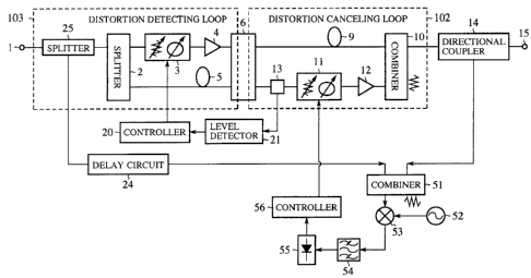
Fig. 5 is a block diagram showing a configuration of an embodiment
1 of the feedforward ampli.f:ier in accordance with the present invention.
In Fig. 5, the reference :numeral 1 designates an input terminal of
the amplifier; 2 designates a splitter (input side splitter) for
delivering the input signal supplied from the input terminal 1 to two
paths; 3 designates a first vector regulator for electrically
2C1 adjusting the amplitude a:nd phase of the signal passing through the
first path; 4 designates a. main amplifier for amplifying the input
signal; 5 designates a delay circuit (a delay circuit in the distortion
detecting loop) for delaying the input signal that is delivered by
the splitter 2 and passes through the second path; and 6 designates
2 5 a splitter/combiner for dividing a part of the output signal of the
main amplifier 4, for supplying a first part of that signal to the
delay circuit. 9, and for combining a second part of the signal and
the part of the input 'signal passing through the delay circuit 5 to
be supplied t:o a directional coupler 1.3.
30 The reference numeral. 103 designates a distortion detecting loop
CA 02347811 2001-04-20
17
comprising the splatters 2 and 25, the first vector regulator 3, the
main amplifier 4, the delay circuit 5 and the splitter/combiner 6.
It cancels out ~~he input signal- component by combining the input signal
with the output of the ma:Ln amplifier 4, thereby extracting the
distortion component of tlZe main amplifier 4.
The reference numeral. 9 designates the delay circuit; 10
designates a c:ombiner; 1.1 designates a second vector regulator; 12
designates an auxiliary amplifier; 13 designates the directional
coupler for era racting part of the output signal; 102 designates a
distortion canceling loop comprising the delay circuit 9, the combiner
10, the second vector regulator 11, the auxiliary amplifier 12 and
the directional coupler 13. The reference numeral 14 designates a
directional coupler; and 15 designates an output terminal of the
amplifier. The reference numeral 20 designates a controller for
controlling the first vector regulator 3; 21 designates a level
detector; 24 d.=signates a delay circuit for delaying the input signal
extracted by a splatter 25; and 25 designates the splatter (first
splatter) for extracting a part of the input signal.
The reference numeral 51 designates a combiner for combining
2 0 the input signal delayed by whe delay circuit 24 with the output signal
extracted by i~he directional coupler 14; 52 designates a local
oscillator fo_= generating a signal of a prescribed frequency; 53
designates a i=requency c:o:nverter for down-converting the output of
the combiner 51 to a low frequency signal using the signal output from
the local oscillator 52; 54 designates a filter (first filter), a
bandpass filter for rejecting the signal component and for passing
the distortion component of the signal output from the frequency
converter 53; 55 designates a power detector (distortion component
detector) for measuring the distortion component output from the
filter 54; and 56 designates a controller (second vector regulator
CA 02347811 2001-04-20
18
controller) for controlling the second vector regulator 11 of the
distortion canceling loop 1.02 such that the distortion component
detected by the power detector 55 becomes minimum.
Next, the operation of the present embodiment 1 will be
described.
In the present embodiment 1 of the feedforward amplifier, the
output signal of the main amplifier 4 passes through the
splitter/combiner 6, and the major part thereof passes through the
delay circuit 9 to be supplied to the first input terminal of the
combiner 10 installed on i~he output side. The distortion component
extracted by the distortion detecting loop 103 appears at a terminal
of the splitter/combine:e° 6, passes through the directional coupler
13 and second vector regulator 11, and is amplified by the auxiliary
amplifier 12 t.o be input to the second input terminal of the combiner
10. The combiner 10 combines the output signal passing through the
delay circuit 9 with the distortion component amplified by the
auxiliary amp7_ifier 12 in i:he same amplitude but in the opposite phase
to cancel the distortion component, thereby producing the output with
little distortion from the output terminal 15.
The feedforward amplifier carries out the optimizing control
of the distortion detecting loop 103 as follows by controlling the
vector regulator 3.
Specifically, the level detector 21 detects the distortion
component signal extracted by the directional coupler 13, and the
controller 20 controls the first vector regulator 3 such that the power
level of the distortion <component becomes minimum. Thus, the optimum
control of the distortion detecting loop 103 is carried out. In this
case, the directional coupler 13 can be installed after the auxiliary
amplifier 12 without any problem.
On the other hand, the combiner 51 is supplied with the part
CA 02347811 2001-04-20
19
of the signal extracted by t:he splitter 25 installed at the input side
of the feedfor'aard amplifier via the delay circuit 24. The combiner
51 is also supplied with t:he part of the output signal of the
feedforward amplifier from. the directional coupler 14 on the output
side. Thus, the combiner 51 combines the output signal of the
feedforward amplifier supplied from the directional coupler 14 with
the input signal extracted by the splitter 25 installed at the input
side. By combining the :input signal with the output signal in the
opposite phases but with the same amplitude, the signal component of
the output signal of the feedforward amplifier is canceled out, leaving
only the distortion component.
The delay circuit 24 is installed to place the input signal and
the output signal in the opposite phase but in the same amplitude at
the combiner 51.
To bring the input signal and output signal in the opposite phase
but in the same amplitude perfectly at the combiner 51 is difficult
because of the accuracy of the circuit components. It is practical
to assume that the signal component is canceled out by a factor of
about 30 dB. The ratio oj= the signal component to the distortion
component of the feedfo.r~,rard amplifier is from 50 dB to 60 dB.
Accordingly, the signal component is greater than the distortion
component by 20 dB to 30 dB even at the output of the combiner 51.
Taking account of this, the frequency converter 53 down-converts the
output of the combiner 51 to a sufficiently lower frequency using the
2'.~ output of the local osc:i_llator 52, and the filter 54, rejecting the
signal component and passing the distortion component, extracts only
the distortion component. The power of the distortion component is
detected by the power detector 55. When the power of the distortion
component is minimum, the distortion canceling loop 102 is adjusted
to the optimum state of the feedforward distortion compensation system.
CA 02347811 2001-04-20
Therefore, the controlle:r_ .'~6 controls the second vector regulator 11
such that the power detected by the power detector 55 becomes minimum.
Incidentally, it is very difficult to fabricate a filter capable
of extracting only the distortion component directly from the radio
5 frequency output of the combiner 51 without down-converting it.
As described above, ~sinr_e the present embodiment 1 does not use
the pilot signal, the pilot signal is not produced from the output
terminal 15. ~Chus, the present embodiment 1 can obviate the filter
for eliminating the pilot signal, and offers an advantage of being
10 able to miniai~urize the feectforward amplifier with ease.
In addition, since t:he present embodiment 1 can prevent the
efficiency of the amplifiE~r from being decreased by the loss of the
filter, it can configure a high efficiency amplifier, thereby offering
an advantage of being able t:o promote the miniaturization and improve
1~~ the efficiency of devices. utilizing the feedforward amplifier.
Furthermore, since l~he present embodiment 1 cancels out the
signal component by the combiner 51 that combines the input signal
extracted by t:he sputter 25 with the output signal extracted by the
directional coupler 14, the power difference between the frequency
20 components of the signal and of the distortion passing through the
filter 54 can be a feasible value from 30 dB to 40 dB, for example.
Thus, it offers an advantage of being able to implement the feedforward
amplifier enabling the reduction in its size and cost.
Moreover, since the present embodiment 1 detects the power of
2.5 the distortic>n component using the low frequency filter 54 after
down-converting the radio-frequency signal to the low frequency by
the frequency converter .53, it is unnecessary to achieve signal
suppression of about 60 dB in the radio frequency as the feedforward
amplifier of Figs. 3 and 4, but the suppression of about 30 dB is
sufficient. Therefore, t:ne multi-stage signal suppressor 22 as shown
CA 02347811 2001-04-20
21
in Fig. 4 is not required, offering an advantage of being able to
implement a small size, pnaci~ical feedforward amplifier.
In addition, the present: embodiment 1 can easily cope with the
frequency change in amplification by varying the oscillation
frequency of the local os<:il.lator 52. In this case, employing a
voltage controlled oscill.at:or (VCO) as the local oscillator 52 enables
the oscillation frequency 1:o be electrically controlled easily,
offering an advantage of being able to implement a feedforward
amplifier that can flexibly deal with the change in the amplification
frequency.
EMBODIMENT 2
Fig. 6 is a block diagram showing a configuration of an embodiment
2 of the feedforward amp:l_ifier. In Fig. 6, the same or like portions
to those of Fig. 5 are designated by the same reference numerals, and
the description thereof is omitted here. In Fig. 6 , the reference
numeral 57 designates a spl.itter (second sputter) interposed between
the combiner 5~1 and the filter 54 for dividing the signal; 58 designates
a filter (second filter), a bandpass filter for rejecting the
2C1 distortion component and passing the signal component of the signal
delivered by t:he splitter 57; 59 designates a power detector (signal
component detector) for measuring the power of the signal component
output from the filter .'~8; 60 designates a controller (third vector
regulator cons:roller) for controlling a third vector regulator 61 such
that the signal component:measured by the power detector 59 becomes
minimums and 61 designates the third vector regulator.
Next, the operation. of the present embodiment 2 will be
described.
A part of the input. signal divided by the splitter 25 passes
through the delay circuit 24 and the third vector regulator 61 to be
CA 02347811 2001-04-20
22
supplied to the combiner 51. The combiner 51 combines the input signal
with the output signal extracted by the directional coupler 14, and
the frequency ~Jonverter 'i3 down-converts the output of the combiner
51. The splitt~er 57 delivers a first part of the output of the frequency
converter 53 tc the filter 54 that passes only the distortion component
to be detected by the power detector 55.
The splitter 57 suppl_Les a second part of the output to the filter
58 so that the :power detector 59 detects the power level of the signal
component.
To improve the accuracy of the cancellation of the signal
component by the combiner 51 that combines the input signal with the
output signal for the cancellation, the controller 60 controls the
third vector regulator 61 such that the power level detected by the
power detector 59 becomes minimum.
As for t)ze distortion component, on the other hand, the power
detector 55 detects its pocaer level and supplies it to the controller
56 that controls the second vector regulator 11 such that the power
level becomes minimum. 'rhe control of the second vector regulator
11 by the controller 56 i:~ carried out independently of the control
of the third vector regulator 61 by the controller 60.
Although the third vector regulator 61 is installed on the path
on the input :>ignal side, it can be interposed into the path on the
output signal side from the directional coupler 14.
As described above, t:he present embodiment 2 can achieve similar
2 _'i advantages of the embodiment 1. In addition, it can always carry out
the cancellation of the ~~ignal component at high accuracy by the
combiner 51 u:~ing the input. signal and output signal, in spite of the
changes in the characteristics of the splitter 25, delay circuit 24,
directional coupler 14 and combiner 51 due to the deterioration with
3 0 age or ambient: temperature variations . Thus, the present embodiment
CA 02347811 2001-04-20
23
2 can reduce the residual signal component due to insufficient
cancellation t.o a favorab7_e level, and reduce the (adverse) effect
of the residual signal component on the power detection of the
distortion component by the power detector 55. Therefore, the power
detector 55 can detect the power of the distortion component at high
detection accuracy, and the controller 56 can control the second vector
regulator 11 :satisfactorily, thereby always maintaining the
feedforward d~~stortion c:o:mpensation at a good condition.
Furthermore, even when the frequency of the amplification
changes, since the frequency characteristics of the splitter 25, delay
circuit 24, directional c~oupl.er 14 and combiner 51 can be compensated
for by adjusting the third vector regulator 61, the combiner 51 can
always cancel the signal component at high accuracy, thereby
implementing ;satisfactory feedforward distortion compensation.
1 ~~
EMBODIMENT 3
Fig. 7 is a block diagram showing a configuration of the present
embodiment 3 of the feedf:orward amplifier. In Fig. 7, the same or
like portions to those of Fig. 6 are designated by the same reference
2 0 numerals, and the description thereof is omitted here.
The present embod.isnent. 3 of the feedforward amplifier is
configured by eliminating the filter 58 for passing the signal
frequency component from the configuration as shown in Fig. 6.
Next, the operation of the present embodiment 3 will be
2.'~ described.
The accuracy of the cancellation of the signal component by the
combiner 51 is determined by the accuracy of the components of the
system, and is about 30 dB at best. Accordingly, the signal component
occupies the major portion of the output of the frequency converter
3 0 53. As a result, it usually presents little problem to eliminate the
CA 02347811 2001-04-20
24
filter for passing only the signal component from before the power
detector 59 for detecting the power level of the signal component.
Thus, the configuration as shown in Fig. 7 that removes the filter
58 for passing the signal frequency component from the configuration
as shown in Fig. 6 can not OIl_Ly achieve the advantages of the foregoing
embodiment 2, but also of~fe:r an advantage of being able to implement
the reduction in size arid cost of the feedforward amplifier.
EMBODIMENT 4
Fig. 8 is a block diagram showing a configuration of the present
embodiment 4 of the feedforward amplifier. In Fig. 8, the same or
like portions to those of Fig. 7 are designated by the same reference
numerals, and the descriptian thereof is omitted here. In Fig. 8,
the reference numeral 62 designates a splitter (second splitter) for
dividing the output of the combiner 51; and 63 designates a
radio-frequency power detector (signal component detector) for
detecting the power of th,e signal delivered by the splitter 62.
Next, the operation of the present embodiment 4 will be
described.
The output of the combiner 51 is divided by the splitter 62,
and the first part thereof= is supplied to the frequency converter 53
that down-converts it to the low frequency. The low frequency signal
passes through the filter_ 54 for passing the distortion component
frequency and is supplied to the power detector 55 so that the
2.'~ controller 56 controls th.e second vector regulator 11 such that the
power level of the distortion component detected by the power detector
55 becomes minimum.
The second part delivered by the splitter 62 is directly supplied
to the radio-f=requency power detector 63 that detects its power level.
The controller 60 contro:Ls the third vector regulator 61 such that
CA 02347811 2001-04-20
the power level. becomes minimum to reduce the signal component in the
output of the c:ombiner 51, thereby improving the detection accuracy
of the distortion component: by the level detector 21.
As described in the foregoing embodiment 3, although the signal
5 component in the output of whe combiner 51 is canceled to some extent,
it still occupies the ma_jo:r portion of the output. Accordingly, the
present embodiment 4 direct:l_y detects the output power of the combiner
51 in the radio frequency band, and controls the third vector regulator
61 such that the power becomes minimum. Thus, the present embodiment
10 4 can implement the canc::ellation of the signal component by the
combiner 51 at practical accuracy, offering an advantage of being able
to provide the feedforward amplifier capable of controlling the
feedforward distortion compensation system at high accuracy.
15 EMBODIMENT 5
Fig. 9 is a block diagram showing a configuration of the present
embodiment 5 of the feedf~arward amplifier. In Fig. 9, the same or
like portions to those of_ Eig. 6 are designated by the same reference
numerals, and the description thereof is omitted here. In Fig. 9,
2 0 the reference numeral 64 designates a frequency converter (second
frequency converter) for down-converting the output signal split by
the directional coupler 14 to a low frequency using the signal output
from the local osc:illator 52; 65 designates a frequency converter
(first frequency converter) for down-converting the output of the
2 5 third vector regulator 61 to a low frequency using the signal output
from the local oscillator 52; and 66 designates a combiner for
combining thE: outputs c~f the frequency converters 64 and 65.
Next, the operation of the present embodiment 5 will be
described.
A part of the input. signal divided by the splitter 25 passes
CA 02347811 2001-04-20
26
through the delay circuit 24 and the third vector regulator 61, and
is down-converted to the 7_ow frequency signal by the frequency
converter 65.
On the other hand, a part of the output signal extracted by the
directional coupler 14 is down-converted to the low frequency signal
by the frequently converter 64. The combiner 66 combines the outputs
of the frequency converters 64 and 65 in the same amplitude but in
the opposite phase to cancf=1 out the signal component. The output
signal of the c:ombiner 66 is divided into two portions by the splitter
57. The first portion passes through the filter 54 that passes only
the distortion component: frequency, and is supplied to the power
detector 55. 'The second pardon passes through the filter 58 that
passes only the signal component frequency, and is supplied to the
power detector 59.
As in the embodiment 1. described before, the controllers 56 and
60 control they second vector regulator. 11 and third vector regulator
61, respectively.
The pre~;ent embodiment 5 of the feedforward amplifier differs
from the foregoing embodiment 2 in that the combiner 66 combines the
2 0 two low frequency signals, that is, the input signal divided by the
splitter 25 ar.,d the output signal extracted by the directional coupler
14, to extract the distortion component by canceling out the signal
component. Accordingly, the combiner 66 can be a combiner for the
low frequency.
As described above, the present embodiment 5 offers the same
advantages of the foregoing embodiment 2. In addition, it can obviate
the radio-frequency connecting wire on the :input side of the combiner
66, thereby offering ar~<~dvantage of being able to provide greater
flexibility of wiring, and by extension to miniaturize the device.
3 0 Furthermore, the present embodiment 5 can implement the circuit
CA 02347811 2001-04-20
27
configuration using the low frequency combiner 66, splitter 57 and
filters 54 and 58, making :it. easier to integrate them into an IC. Thus,
it offers an advantage c:~f being able to implement the feedforward
amplifier that. can reduce its size and cost with ease.
EMBODIMENT 6
Fig. 10 is a block diagram showing a configuration of the present
embodiment 6 of the feedforward amplifier. In Fig. 10, the same or
like portions to those of Fig. 9 are designated by the same reference
numerals, and the descrz.pti.on thereof is omitted here. In Fig. 10,
the reference numeral 6'7 designates a frequency converter (first
frequency converter) for down-converting a part of the input signal
divided by the sputter 2'i by using the output signal from the local
oscillator 52; 68 designates a low frequency delay circuit for delaying
1_'> the output of the frequency converter 67; and 69 designates a low
frequency vecJ~or regulator for adjusting the pass amplitude and pass
phase of the output of the delay circuit 68.
The present embodiment 6 of the feedforward amplifier differs
from the foregoing embodiment 5 in that the part of the input signal
21) divided by th~~ input side ;splitter 25 is immediately down-converted
to the low frequency by i~he frequency converter 67. The output of
the frequency converter. n'7 passes through the low frequency delay
circuit 68 anc~ the low frequency vector regulator 69, and is supplied
to the combiner 66. The subsequent operation is the same as that of
2 5 the foregoing embodiment 5.
As described above, the present embodiment 6 can achieve the
same advantages as the foregoing embodiment 5. In addition, the
present embodiment 6 can utilize low frequency components for the delay
circuit 68 and the vector_ regulator 69, which are fabricated easier
30 than those o:f the radio-frequency counterparts. In addition, the
CA 02347811 2001-04-20
28
vector regulator can be configured using a signal processing circuit
(DSP: Digital Signal Proce:~sor) which can provide greater flexibility
to the vector regulator, making it easier to miniaturize and adjust
the vector regulator, and by extension to reduce the size of the
feedforward amplifier and to improve the distortion characteristic.
Furthermore, since a7_1 the circuit components following the
frequency converters 64 and 67 are low frequency components, it
possible to integrate them .into an IC including the controller 56 for
controlling the distortion canceling loop 102 (that is, the second
vector regulator 11) of the feedforward distortion compensation
circuit. Thus, the present embodiment 6 offers an advantage of being
able to implement the feediorward amplifier with a reduced size and
cost.
EMBODIMENT 7
Fig. 11 is a block diagram showing a configuration of the present
embodiment 7 of the feedforward amplifier. In F.ig. 11, the same or
like portions to those of Fig. 6 are designated by the same reference
numerals, and the description thereof is omitted here. In Fig. 11,
2 0 the reference numeral 71 designates a splatter (first splatter)
interposed between the sputter 2 and the delay circuit 5 for further
dividing the part of the input signal divided by the splatter 2.
The present embodim~ant 7 of the feedforward amplifier differs
from the foregoing embodiment 2 in that it comprises the splatter 71,
which is interposed between the sputter 2 and the delay circuit 5
for further dividing the part of the input signal divided by the
splatter 2, instead of the splatter 25 for dividing the input signal
supplied from the input:: terminal 1.
The foregoing configuration can remove the splatter 25 from the
main path of the input signal from t;he input terminal 1 to the
CA 02347811 2001-04-20
29
splitter/combiner 6 via tr.e main amplifier 4, that is, the path of
the major part of the signal to become the output signal of the
feedforward amplifier, thereby preventing the reduction in the total
gain of the amplifier due too the loss of the sputter 25.
Although the configuration of Fig. 11 changes the position of
the splitter 25 for divi.d_Lng the input signal in the foregoing
embodiment 2, t:he foregoi.nc~ embodiments 1, and 3-6 can also offer the
same advantage as the present: embodiment 7 by changing the position
of their splitaer 25.
EMBODIMENT 8
Fig. 12 is a block diagram showing a configuration of the present
embodiment 8 of the feedforward amplifier. In Fig. 12, the same or
like portions to those of: Fig. 6 are designated by the same reference
numerals, and the description thereof is omitted here. In Fig. 12,
the reference numeral 7? designates a splitter interposed into the
path on the output side o:~ the delay circuit 5 for further dividing
a part of the input signal. divided by the splitter 2 and passing through
the delay circuit 5.
The present embodiment 8 of the feedforward amplifier differs
from the foregoing embodinnent 2 in that it comprises the splitter 72,
which is interposed into the path on the output side of the delay
circuit 5 for further dividing the part of the input signal divided
by the splitter 2 and pa~~sing through the delay circuit 5, instead
of the splitter 25 for dividing the input signal supplied from the
input terminal 1.
This configuration makes it possible for the delay circuit 5
to share the function of the delay circuit 24 in part, reducing the
delay time of: the delay circuit 24. Thus, it is possible to reduce
the size of the delay ci.rc~uit 24, and by extension to reduce the size
CA 02347811 2001-04-20
of the device.
Although the configuration of Fig. 12 utilizes the splitter 72
interposed into the path cn. the output side of the delay circuit 5
in place of the spl.itter L'.5 for dividing the input signal in the
5 foregoing embodiment 2, t:he foregoing embodiments l, and 3-6 can also
offer the same advantage as the present embodiment 8 by changing the
position of their splitter 25 to the output side of the delay circuit
5.
10 INDUSTRIAL APF?LICABILIT~.'
As described above, the feedforward amplifier in accordance with
the present invention can be preferably applied to the low distortion
amplification in a radio frequency band such as VHF, UHF and microwave
frequency bands for implementing favorable distortion compensation
15 without being affected by the ambient temperature or deterioration
with age.