Note: Descriptions are shown in the official language in which they were submitted.
CA 02347869 2001-04-24
13..
1
LINKED BRIDGE
BACKGROUND OF THE INVENTION
1. Field of the Invention
The present invention relates to data processing systems, and more
particularly, to bridge systems including mechanisms for transferring
information
between buses.
2. Description of Related Art
Computers can use buses to transfer data between a host processor and
various devices, such as memory devices and input/output devices. As used
herein an "input/output" device is a device that either generates an input or
receives an output (or does both). Thus "input/output" is used in the
15 disjunctive. These buses may be arranged in a hierarchy with the host
processor
connected to a high level bus reserved for exchanging the data most urgently
needed by the processor. Lower level buses may connect to devices having a
lower priority.
20 Other reasons exist for providing separate buses. Placing an excessive
number of devices on one bus produces high loading. Such loading makes a
bus difficult to drive because of the power needed and the delays caused by
signaling so many devices. Also, some devices on a bus may periodically act
as a master and request control over a bus in order to communicate with a
slave
25 - device. By segregating some devices on a separate bus, master devices can
communicate with other devices on the lower level bus without tying up the bus
used by the host processor or other masters.
The PCI bus standard is specified by the PCI Special Interest Group of
30 Hillsboro, Oregon. The PCI bus features a 32-bit wide, multiplexed address-
data
(AD) bus portion, and can be expanded to a 64-bit wide AD bus portion.
CA 02347869 2001-04-24
2
Maintaining a high data throughput rate (e.g., a 33 MHZ clock rate) on the PCI
bus leads to a fixed limitation on the number of electrical AC and DC loads on
the bus. Speed considerations also limit the physical length of the bus and
the
capacitance that can be placed on the bus by the loads, while future PCI bus
rates (e.g., 66 MHZ) will exacerbate the electrical load and capacitance
concerns. Failure to observe these load restrictions can cause propagation
delays and unsynchronized operation between bus devices.
To circumvent these loading restrictions, the PCI bus standard specifies
a bridge to allow a primary PCI bus to communicate with a secondary PCI bus
through such a bridge. Additional loads may be placed on the secondary bus
without increasing the loading on the primary bus. For bridges of various
types
see U.S. Patents 5,548,730 and 5,694,556.
15 The PCI bridge observes a hierarchy that allows an initiator or bus master
on either bus to complete a transaction with a target on the other bus. As
used
herein, hierarchy refers to a system for which the concept of a higher or
lower
level has meaning. For example, a PCI bus system is hierarchical on several
scores. An ordering of levels is observed in that a high level host processor
normally communicates from a higher level bus through a bridge to a lower
level
bus. An ordering of levels is also observed in that buses at equal levels do
not
communicate directly but through bridges interconnected by a higher level bus.
Also, an ordering of levels is observed in that data is filtered by their
addresses
before being allowed to pass through a bridge, based on the levels involved.
25 Other hierarchical systems exist that may observe an ordering of levels by
using
one or more of the foregoing concepts, or by using different concepts.
Some personal computers have slots for add-on cards, which allow the
card to connect to a peripheral bus in the computer. Because a user often
30 needs additional slots, expansion cards have been designed that will
connect
between .the peripheral bus and an external unit that offers additional slots
for
CA 02347869 2001-04-24
3
add-on cards. For systems for expanding a bus, see U.S. Patents 5,006,981;
5,191,657; and 5,335,329. See also U.S. Patent 5,524,252.
For portable computers, special considerations arise when the user
wishes to connect additional peripheral devices. Often a user will brino a
portable computer to a desktop. and connect through a docking station or port
replicator to a keyboard, monitor, printer or the like. A user may also wish
to
connect to a network through a network interface card in the docking station.
At times, a user may need additional devices such as hard drives or CD-ROM
10 drives. While technically possible to a limited extent, extending a bus
from a
portable computer through a cable is difficult because of the large number of
wires needed and because of latencies caused by a cable of any significant
length.
In U.S. Patent 5,696,949 a host chassis has a PCI to PCI bridge that
connects through a cabled bus to another PCI to PCI bridge in an expansion
chassis. This system is relatively complicated since two independent bridges
communicate over a cabled bus. This cabled bus includes essentially all of the
lines normally found in a PCI bus. This approach employs a delay technique to
20 deal with clock latencies associated with the cabled bus. A clock signal
generated on the expansion side of the cabled bus: (a) is sent across the
cabled
bus, but experiences a delay commensurate with the cable length; and (b) is
delayed an equivalent amount on the expansion side of the cabled bus by a
delay line there, before being used on the expansion side. Such a design
25 complicates the system and limits it to a tuned cable of a pre-designed
length,
making it difficult to accommodate work spaces with various physical layouts.
U.S. Patent 5,590,377 shows a primary PCI bus in a portable computer
being connected to a PCI to PCI bridge in a docking station. When docked, the
30 primary and secondary buses are physically very close. A cable is not used
to
allow separation between the docking station and the portable computer. With
CA 02347869 2001-04-24
i
4
this arrangement, there is no interface circuitry between the primary PCI bus
and the docking station. See also U.S. Patent 5,724,529.
U.S. Patent 5,540,597 suggests avoiding additional PCMCIA connectors
when connecting a peripheral device to a PC card slot in a portable computer,
but does not otherwise disclose any relevant bridging techniques.
U.S. Patents 4,882,702 and show a programmable controller for
controlling industrial machines and processes. The system exchanges data
10 serially with a variety of input/output modules. One of these modules may
be
replaced with an expansion module that can serially communicate with several
groups of additional input/output modules. This system is not bridge-like in
that
the manner of communicating with the expansion module is different than the
manner of communicating with the input/output modules. For the expansion
module the system changes to a block transfer mode where a group of status
bytes are transferred for all the expansion devices. This system is also
limited
to input/output transactions and does not support a variety of addressable
memory transactions. See also U.S. Patent 4,413,319; and 4,504,927.
In U.S. Patent 5,572,525 another bus designed for instrumentation (IEEE
488 General Purpose Instrumentation Bus) connects to an extender that breaks
the bus information into packets that are sent serially through a transmission
cable to another extender. This other extender reconstructs the serial packets
into parallel data that is applied to a second instrumentation bus. This
extender
25 is an intelligent system operating through a message interpretation layer
and
several other layers before reaching the parallel to serial conversion layer.
Thus
this system is unlike a bridge. This system is also limited in the type of
transactions that it can perform. See also U.S. Patent 4,959,833.
U.S. Patent 5,325,491 shows a system for interfacing a local bus to a
cable with a large number of wires for interfacing with remote peripherals.
See
CA 02347869 2001-04-24
also U.S. Patents 3,800,097; 4,787,029; 4,961,140; and 5,430,847.
The Small Computer System Interface (SCSI) defines bus standards for
a variety of peripheral devices. This SCSI bus is part of an intelligent
system
5 that responds to high-level commands. Consequently, SCSI systems require
software drivers to enable hardware to communicate to the SCSI bus. This
fairly complicated system is quite different from bridges such as bridges as
specified under the PCI standard. A variety of other complex techniques and
protocols exist for transferring data, including Ethernet, Token Ring, TCP/IP,
ISDN, FDDI, HIPPI, ATM, Fibre Channel, etc., but these bear little relation to
bridge technology.
See also U.S. Patents 4,954,949; 5,038,320; 5,111,423; 5,446,869;
5,495,569; 5,497,498; 5,507,002; 5,517,623; 5,530,895; 5,542,055;
15 5,555,510; 5,572,688; and 5,61 1,053.
Accordingly, there is a need for an improved system for transferring
information between buses.
SUMMARY OF THE INVENTION
In accordance with the illustrative embodiments demonstrating features
and advantages of the present invention, there is provided a bridge accessible
by a host processor for expanding access over a first bus to a second bus. The
first bus and the second bus are each adapted to separately connect to
respective.ones of a plurality of bus-compatible devices. Allowable ones of
the
devices include memory devices and input/output devices. The bridge has a
link, together with a first and a second interface. The first interface is
adapted
to couple between the first bus and the link. The second interface is adapted
30 to couple between the second bus and the link. The first interface and the
second interface operating as a single bridge are operable to (a) send
outgoing
CA 02347869 2001-04-24
i
6
information serially through the link in a format different from that of the
first
bus and the second bus without waiting for an incoming acknowledgement over
said link before inaugurating a transfer of said information over said link,
(b)
approve an initial exchange between the first bus and the second bus in
5 response to a pending transaction having a characteristic signifying a
destination
across the bridge, and (c) allow the host processor, communicating through the
first bus, to individually address different selectable ones of the bus-
compatible
devices on the second bus, including memory devices and input/output devices
that may be present: (i) using on the first bus substantially the same type of
10 addressing as is used to access devices the first bus, and (ii) without
first
employing a second, intervening one of the bus-compatible devices on the
second bus.
In accordance with another aspect of the invention a bridge accessible by
15 a host processor can expand access over a first bus to a second bus. The
first
bus and the second bus each are adapted to separately connect to respective
ones of a plurality of bus-compatible devices. Allowable ones of the devices
include memory devices and input/output devices. The bridge has a link,
together with a first and a second interface. The first interface is adapted
to
20 couple between the first bus and the link. The second interface is adapted
to
couple between the second bus and the link. The first interface and the second
interface are operable to (a) send information serially through the link in a
format different from that of the first bus and the second bus, (b) exchange
information between the first bus and the second bus according to a
25 predetermined hierarchy giving the first bus a higher level than the second
bus,
and (c) allow the host processor, communicating through the first bus, to
individually address different selectable ones of the bus-compatible devices
on
the second bus, including memory devices and input/output devices that may
be present: (i) using on the first bus substantially the same type of
addressing
30 as is used to access devices on the first bus, (ii) without first employing
a
second, intervening one of the bus-compatible devices on the second bus, and
CA 02347869 2001-04-24
7
(iii) without passing the information through an intewening hierarchical
level.
In accordance with another, further aspect of the invention a bridge
accessible by a processor can expand access over a first bus to a second bus.
The first bus and the second bus each are adapted to separately connect to
respective ones of a plurality of.bus-compatible devices. The bridge has a
link
and a first and a second interface. The first interface is coupled between the
first bus and the link. The second interface is adapted to couple between the
second bus and the link. The first interface and the second interface operate
as a single bridge and is operable to transfer information serially through
the link
in a format different from that of the first bus and the second bus without
waiting for an incoming acknowledgment over the link before inaugurating a
transfer of the information over the link.
By employing apparatus and methods of the foregoing type, an improved
system is achieved for transferring information between buses. In one
preferred
embodiment, two buses communicate over a duplex link formed with a pair of
simplex links, each employing twisted pair or twin axial lines (depending on
the
desired speed and the anticipated transmission distance). Information from the
buses are first loaded onto FIFO (first-in first-out) registers before being
serialized into frames for transmission over the link. Received frames are
deserialized and loaded into FIFO registers before being placed onto the
destination bus. Preferably, interrupts, error signals, and status signals are
sent
along the link.
In this preferred embodiment, address and data are taken from a bus one
transaction at a time, together with four bits that act either as control or
byte
enable signals. Two or more additional bits may be added to tag each
transaction as either: an addressing cycle; acknowledgment of a non-posted
write; data burst; end of data burst (or single cycle). If these transactions
are
posted writes they can be rapidly stored in a FIFO register before being
encoded
CA 02347869 2001-04-24
into a number of frames that are sent serially over' link. When pre-fetched
reads are allowed, the FIFO register can store pre-fetched data in case the
initiator requests it. For single cycle writes or other transactions that must
await a response, the bridge can immediately signal the initiator to wait,
even
before the request is passed to the target.
In a preferred embodiment, one or more of the buses follows the PCI or
PCMCIA bus standard (although other bus standards can be used instead). The
preferred apparatus then operates as a bridge with a configuration register
that
is loaded with information specified under the PCl standard. The apparatus can
transfer information between buses depending upon whether the pending
addresses fall within a range embraced by the configuration registers. This
scheme works with devices on the other side of the bridge, which can be given
unique base addresses to avoid addressing conflicts.
In one highly preferred embodiment, the apparatus may be formed as two
separate application-specific integrated circuits (ASIC) joined by a cable.
Preferably, these two integrated circuits have the same structure, but can act
in two different modes in response to a control signal applied to one of its
pins.
Working with hierarchical buses (primary and secondary buses) these integrated
circuits will be placed in a mode appropriate for its associated bus. The ASIC
associated with the secondary bus preferably has an arbiter that can grant
masters control of the secondary bus. This preferred ASIC can also supply a
number of ports to support a mouse and keyboard, as well as parallel and
serial
25 ports.
When used with a portable computer, one of the ASIC's can be
assembled with a connector in a package designed to fit into a PC card slot
following the PCMCIA standard. This ASIC can connect through a cable to the
30 other ASIC, which can be located in a docking station. Accordingly, the
apparatus can act as a bridge between a CardBus and a PCI bus located in a
CA 02347869 2001-04-24
9
docking station. Since the preferred ASIC can also~~~rovide a port for a mouse
and keyboard, this design is especially useful for a docking station. Also,
the
secondary PCI bus implemented by the ASIC can connect to a video card or to
a video processing circuit on the main dock circuit board in order to drive a
monitor.
In some embodiments, one ASIC will be mounted in the portable
computer by the original equipment manufacturer (OEM). This portable
computer will have a special connector dedicated to the cable that connects to
10 the docking station with the mating ASIC. For such embodiments, the
existence within the preferred ASIC of ports for various devices can be highly
advantageous. An OEM can use this already existing feature of the ASIC and
thereby eliminate circuitry that would otherwise have been needed to implement
such ports.
BRIEF DESCRIPTION OF THE DRAWINGS
The above brief description as well as other objects, features and
20 advantages of the present invention will be more fully appreciated by
reference
to the following detailed description of presently preferred but nonetheless
illustrative embodiments in accordance with the present invention when taken
in conjunction with the accompanying drawings, wherein:
25 Figure 1 is a schematic block diagram showing a bridge split by a link
within the bridge, in accordance with principles of the present invention;
Figure 2 is a schematic block diagram showing a bridge in accordance
with principles of the present invention using the link of Figure 1;
Figure 3 is a schematic block diagram showing the bridge of Figure 2
CA 02347869 2001-04-24
10
used in a docking system in accordance with principles of the present
invention;
Figure 4 is a cross-sectional view of the cable of Figure 3;
5 Figure 5 is a schematic illustration of the bridge of Figure 3 shown
connected to a portable computer and a variety of peripheral devices; and
Figure 6 shows a docking station similar to that of Figure 5 but with the
portable computer modified to contain an application-specific integrated
circuit
10 designed to support a link to the docking station.
CA 02347869 2001-04-24
11
DETAILED DESCRIPTION OF THE PREFERRED EMBODIMENTS
Referring to Figure 1, a bridge is shown connecting between a first bus
and a second bus 12 (also referred to as primary bus 10 and secondary bus
5 12). These buses may be PCI or PCMCIA 32-bit buses, although other types
of buses are contemplated and.the present disclosure is not restricted to any
specific type of bus. Buses of this type will normally have address and data
lines. In some cases, such as with the PCI bus, address and data are
multiplexed onto the same lines. In addition, these buses will have signaling
10 lines for allowing devices on the bus to negotiate transactions. For the
PCI
standard, these signaling lines will include four lines that are used either
for
control or byte enabling (C/BE[3:0]). Others signaling lines under the PCI
standard exist for gaining control over the bus, for handshaking, and the like
(e.g., FRAME#, TRDY#, IRDY#, STOP#, DEVSEL#, etc.)
Buses 10 and 12 are shown connecting to a first interface 14 and second
interface 16, respectively (also referred to as interfaces 14 and 16). Bus
information selected for transmission by interfaces 14 and 16 are loaded into
registers 18 and 20, respectively. Incoming bus information that interfaces 14
20 and 16 select for submission to the buses are taken from registers 22 and
24,
respectively. In one embodiment, registers 18-24 are each 16 X 38 FIFO
registers, although different types of registers having different dimensions
may
be used in alternate embodiments.
25 In this embodiment, registers 18-24 are at least 38 bits wide. Thirty six
of those bits are reserved for the 4 control bits (C/BE#[3:0]) and the 32
address/data bits (AD[31:0)) used under the PCI bus standard. The remaining
two bits can be used to send additional tags for identifying the nature of the
transaction associated therewith. Other bits may be needed to fully
characterize
30 every contemplated transaction. Transactions can be tagged as: addressing
cycle; acknowledgment of a non-posted write; data burst; end of data burst (or
CA 02347869 2001-04-24
12
single cycle). Thus outgoing write transactions can ~be tagged as a single
cycle
transaction or as part of a burst. Outgoing read requests can also be tagged
as
part of a burst with a sequence of byte enable codes (C/BE) for each
successive
read cycle of the burst. It will be appreciated that other coding schemes
using
a different number of bits can be used in other embodiments.
The balance of the structure illustrated in Figure 1 is a link designed to
establish duplex communications between interfaces 14 and 16 through
registers 18-24. For example, encoder 28 can accept the oldest 38 bits from
register 20 and parse it into five bytes (40 bits). The extra two bits of the
last
byte are encoded to signify the interrupts, status signals and error signals
that
may be supplied from block 34.
Each of these five bytes is converted into a 10 bit frame that can carry
the information of each byte, as well as information useful for regulating the
link. For example, these frames can carry comma markers, idle markers, or flow
control signals, in a well-known fashion. A transceiver system working with
bytes that were encoded into such 10 bit frames is sold commercially by
Hewlett Packard as model number HDMP-1636 or -1646. Frames produced by
encoder 28 are forwarded through transmitter 44 along simplex link 46 to
receiver 48, which supplies the serial information to decoder 30. Likewise,
encoder 26 forwards serial information through transmitter 38 along simplex
link
40 to receiver 42, which supplies the serial information to decoder 32.
Flow control may be necessary should FIFO registers 22 or 24 be in
danger of overflowing. For example, if FIFO register 22 is almost full, it
supplies
a threshold detect signal 36 to encoder 26, which forwards this information
through fink 40 to decoder 32. In response, decoder 32 issues a threshold stop
signal 50 to encoder 28, which then stops forwarding serial information,
thereby preventing an overflow in FIFO register 22. In a similar fashion, a
potential overflow in FIFO register 24 causes a threshold detect signal 52 to
CA 02347869 2001-04-24
13
flow through encoder 28 and link 46 to cause decoder 30 to issue a threshold
stop signal 54, to stop encoder 26 from sending more frames of information.
In some embodiments, the system will examine the received information to
determine if it contains transmission errors or has been corrupted in some
5 fashion. In such event the system can request a retransmission of the
corrupted information and thereby ensure a highly reliable link.
In this embodiment, elements 14, 18, 22, 26, 30, 38 and 48 are part of
a single, application specific integrated circuit (ASIC) 56. Elements 16, 20,
24,
10 28, 32, 42 and 44 are also part of an ASIC 58. As described further
hereinafter, first ASIC 56 and second ASIC 58 have an identical structure but
can be operated in different modes. It will be appreciated that other
embodiments may not use ASIC's but may use instead alternate circuitry, such
as a programable logic device, or the like. As shown herein, ASIC 56 is
15 operating in a mode designed to service primary bus 10, and (for reasons to
be
described presently) will be sending outputs to block 57. In contrast block 34
of ASIC 58 will receive inputs from block 34.
Encoders 26 and 28 have optional parallel outputs 27 and 29,
20 respectively, for applications requiring such information. Also for such
applications, decoders 30 and 32 have parallel inputs 31 and 33, respectively.
These optional inputs and outputs may be connected to an external transceiver
chip, such as the previously mentioned device offered by Hewlett Packard as
model number HDMP-1636 or -1646. These devices will still allow the system
25 to transmit serial information, but by means of an external transceiver
chip.
This allows the user of the ASIC's 56 and 58 more control over the methods
of transmission over the link.
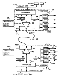
Referring to Figure 2, previously mentioned ASIC's 56 and 58 are shown
30 in further detail. The previously mentioned encoders, decoders,
transmitters,
receivers, and FIFO registers are combined into blocks 60 and 62, which are
CA 02347869 2001-04-24
14
interconnected by a duplex cable formed of previously mentioned simplex links
40 and 46. Previously mentioned interface 14 is shown connected to primary
bus 10, which is also connected to a number of bus-compatible devices 64.
Similarly, previously mentioned interface 16 is shown connected to secondary
5 bus 12, which is also connected to a number of bus-compatible devices 66.
Devices 64 and 66 may be PCI-compliant devices and may operate as memory
devices or input/output devices.
Interface 14 a shown connected to a first register means 68, which acts
as a configuration register in compliance with the PCI standard. Since this
system will act as a bridge, configuration registers 68 will have the
information
normally associated with a bridge. Also, configuration registers 68 will
contain
a base register and limit register to indicate a range or predetermined
schedule
of addresses for devices that can be found on the secondary bus 12. Under the
PCI standard, devices on a PCI bus will themselves each have a base register,
which allows mapping of the memory space and/or I/O space. Consequently,
the base and limit registers in configuration registers 68 can accommodate the
mapping that is being performed by individual PCI devices. The information on
configuration registers 68 are mirrored on second configuration register 67
(also
referred to as a second configuration meansl. This makes the configuration
information readily available to the interfaces on both sides of the link.
In this embodiment, ASIC 58 has an arbiter 70. Arbiters are known
devices that accept requests from masters on secondary bus 12 for control of
the bus. The arbiter has a fair algorithm that grants the request of one of
the
contending masters by issuing it a grant signal. In this hierarchical scheme,
secondary bus 12 requires bus arbitration, but primary bus 10 will provide its
own arbitration. Accordingly, ASIC 56 is placed in a mode where arbiter 72 is
disabled. The modes of ASIC's 56 and 58 are set by control signals applied to
control pins 74 and 76, respectively. Because of this mode selection, the
signal
directions associated with blocks 57 and 34 will be reversed.
CA 02347869 2001-04-24
In this embodiment, ASIC 58 is in a mode that implements a third bus
78. Bus 78 may follow the PCI standard, but is more conveniently implemented
in a different standard. Bus 78 connects to a number of devices that act as a
port means. For example, devices 80 and 82 can implement PS/2 ports that
5 can connect to either a mouse or a keyboard. Device 84 implements an
ECP/EPP parallel port for driving a printer or other device. Device 86
implements a conventional serial port. Devices 80, 82, 84 and 86 are shown
with input/output lines 81, 83, 85 and 87, respectively. Devices 80-86 may be
addressed on bus 10 as if they were PCI devices on bus 12. Also in this
10 embodiment, a bus 88 is shown in ASIC 56, with the same devices as shown
on bus 78 to enable an OEM to implement these ports without the need for
separate input/output circuits.
Referring to Figure 3, previously mentioned ASIC 58 is shown in a
15 docking station 130 connected to an oscillator 91 for establishing a remote
and
internal clock. ASIC 58 has its lines 81 and 83 connected through a connection
assembly 90 for connection to a keyboard and mouse, respectively. Serial lines
85 and parallel lines 87 are shown connected to transceivers 92 and 94,
respectively, which then also connect to connection assembly-90 for connection
20 to various parallel and serial peripherals, such as printers and modems.
ASIC 58 is also shown connected to previously mentioned secondary bus
12. Bus 12 is shown connected to an adapter card 96 to allow the PCI bus 12
to communicate with an IDE device such as a hard drive, backup tape drive, CD-
25 ROM drive, etc. Another adapter card 98 is- shown for allowing
communications from bus 12 to a universal serial port (USB). A network
interface card 100 will allow communications through bus 12 to various
networks operating under the Ethernet standard, Token Ring standard, etc.
Video adapter card 102 (also referred to as a video means) allows the user to
30 operate another monitor. Add-on card 104 may be one of a variety of cards
selected by the user to perform a useful function. While this embodiment
CA 02347869 2001-04-24
16
shows various functions being implemented ~'iay add-on cards, other
embodiments may implement one or more of these function on a common
circuit board in the dock (e.g., all functions excluding perhaps the IDE
adapter
cardl.
ASIC 58 communicates through receiver/transmitter 106, which provides
a physical interface through a terminal connector 108 to cable 40, 46.
Connector 108 may be a 20 pin connector capable of carrying high speed
signals with EMI shielding (for example a low force helix connector of the
type
10 offered by Molex Incorporated), although other connector types may used
instead. The opposite end of cable 40, 46 connects through a gigabit, terminal
connector 1 10 to physical interface 1 12, which acts as a
receiver/transmitter.
Interface 1 12 is shown connected to previously mentioned first ASIC 56, which
is also shown connected to an oscillator 1 14 to establish a local clock
signal.
This specific design contemplates using an external transmitter/receiver
(external SERDES of lines 27, 29, 31, and 33 of Figure 1 ), although other
embodiments can eliminate these external devices in favor of the internal
devices in ASIC's 56 and 58.
20 This embodiment is adapted to cooperate with a portable computer
having a PCMCIA 32-bit bus 10, although other types of computers can be
serviced. Accordingly, ASIC 56 is shown in a package 1 16 having an outline
complying with the PCMCIA standard and allowing package 1 16 to fit into a
slot in a portable computer. Therefore, ASIC 56 has a connector 118 for
connection to bus 10. Cable 40, 46 will typically be permanently connected to
package 1 16, but a detachable connector may be used in other embodiments,
where a user wishes to leave package 1 16 inside the portable computer.
Power supply 120 is shown producing a variety of supply voltages used
to power various components. In some embodiments, one of these supply lines
can be connected directly to the portable computer to charge its battery.
CA 02347869 2001-04-24
17
Referring to Figure 4, the previously mentiori~d simplex links 40 and 46
are shown as twin axial lines 40A and 46A, wrapped with individual shields
40B and 46B. A single shield 122 encircles the lines 40 and 46. Four parallel
wires 124 are shown (although a greater number may be used in other
embodiments) mounted around the periphery of shields 122 for various
purposes. These wires 124 may. carry power management signals, dock control
signals or other signals that may be useful in an interface between a docking
station and a portable computer. While twin axial lines offer high
performance,
twisted pairs or other transmission media may be used in other embodiments
where the transmission distance is not as great and where the bit transfer
speed
need not be as high. While a hard wire connection is illustrated, in other
embodiments a wireless or other type of connection can be employed instead.
Referring to Figure 5, previously mentioned package 1 16 is shown in
position to be connected to a PCMCIA slot in portable computer 126.
Computer 126 is shown having primary bus 10 and a host processor 128.
Package 1 16 is shown connected through cable 40, 46 to previously mentioned
connector 108 on docking station 130. Previously mentioned docking station
130 is shown connecting through PS/2 ports to keyboard 132 and mouse 134.
A printer 136 is shown connected to a parallel port in docking station 130.
Previously mentioned video means 102 is shown connected to a monitor 138.
Docking station 130 is also shown with an internal hard drive 140 connecting
to the adapter card previously mentioned. A CD-ROM drive 142 is also shown
mounted in docking station 130 and connects to the secondary bus through an
appropriate adapter card (not shown). Previously mentioned add-on card 104
is shown with its own cable 144.
Referring to Figure 6, a modified portable computer 126' is again shown
with a host processor 128 and primary bus 10. In this embodiment however,
portable computer 126' contains previously mentioned ASIC 56. Thus there is
no circuitry required (other than perhaps drivers) between ASIC 56 and cable
CA 02347869 2001-04-24
18
40,46. In this case, the laptop end of cable 40, 46 fias a connector 142
similar
to the one on the opposite end of the cable (connector 108 of Figure 5).
Connector 143 is designed to mate with connector 141 and support the high-
speed link. As before, connectors 141 and 143 can also carry various power
management signals, and other signals associated with a docking system.
An important advantage of this arrangement is the fact that ASIC 56
contains circuitry for providing ports, such as a serial port, a parallel
port, PS/2
ports for a mouse and keyboard, and the like. Since portable computer 126'
would ordinarily provide such ports, ASIC 56 simplifies the design of the
portable computer. This advantage is in addition to the advantage of having a
single ASIC design (that is, ASIC's 56 and 58 are structured identically),
which
single design is capable of operating at either the portable computer or the
docking station, thereby simplifying the ASIC design and reducing stocking
requirements, etc.
To facilitate an understanding of the principles associated with the
foregoing apparatus, its operation will be briefly described. This operation
will
be described in connection with the docking system of Figures 3 and 5 (which
generally relates to Figure 2), although operation would be similar for other
types of arrangements. For the docking system, a connection is established by
plugging package 1 16 (Figure 5) into portable computer 126. This establishes
a link between the primary bus 10 and ASIC 56 (Figure 3).
At this time an initiator (the host processor or a master) having access
to primary bus 10 may assert control of the bus. An initiator will normally
send
a request signal to an internal arbiter (not shown) that will eventually grant
control to this initiator. In any event, the initiator asserting control over
primary
bus 10 will exchange the appropriate handshaking signals and drive an address
onto the bus 10. Control signals simultaneously applied to the signaling lines
of bus 10 will indicate whether the transaction is a read, write, or other
type of
CA 02347869 2001-04-24
19
transaction.
Interface 14 (Figure 2) will examine the pending address and determine
whether it represents a transaction with devices on the other side of the
bridge
5 (that is, secondary bus 12) or with the bridge itself. Configuration
register 68
has already been loaded in the usual manner with information that indicates a
range of addresses defining the jurisdiction of the interface 14.
Assuming a write transaction is pending on bus 10, interface 14 will
transfer 32 address bits together with four control bits (PCI standard) to
FIFO
register 18 (Figure 1 ). Encoder 26 will add at least two additional bits
tagging
this information as an addressing cycle. The information is then broken into
frames that can carry flow control and other signals before being transmitted
serially over link 40.
Without waiting, interface 14 will proceed to a data cycle and accept up
to 32 bits of data from bus 10 together with four byte enable bits. As before,
this information will be tagged, supplemented with additional information and
broken into frames for serial transmission over link 40. -This transmirtPr~
information will be tagged to indicate whether it is part of a burst or a
single
cycle.
Upon receipt, decoder 32 restores the frames into the original 38 bit
format and loads the last two described cycles onto the stack of register 24.
Interface 16 eventually notices the first cycle as an addressing cycle in a
write
request. Interface 16 then negotiates control over bus 12 in the usual fashion
and applies the address to bus 12. A device on bus 12 will respond to the
write
request by performing the usual handshaking.
Next, interface 16 will drive the write data stacked on register 24 into
bus 12. If this transaction is a burst, interface 16 will continue to drive
data
CA 02347869 2001-04-24
onto bus 12 by fetching it from register 24. If ho~rvever this transaction is
a
single cycle write, interface 16 will close the transaction on bus 12 and load
an
acknowledgment into register 20. Since this acknowledgment need not carry
data or address information, a unique code may be placed into register 20, so
5 that encoder 28 can appropriately tag this line before parsing it into
frames for
transmission over link 46. Upon. receipt, decoder 30 will produce a unique
code
that is loaded into register 22 and eventually forwarded to interface 14,
which
sends an acknowledgment to the device on bus 10 that the write has
succeeded.
If the initiator instead sets its control bits during the address cycle to
indicate a read request, interface 14 would also accept this cycle, if it has
jurisdiction. Interface 14 will also signal the initiator on bus 10 that it is
not
ready to return data (e.g., a retry signal, which may be the stop signal as
defined under the PCI standard). The initiator can still start (but not
finish) a
data cycle by driving its signaling tines on bus 10 with byte enable
information.
Using the same technique, the address information, followed by the byte enable
information, will be accepted by interface 14 and loaded with tags into
register
18. These two lines of information will be then encoded and transmitted
serially
over link 40. Upon receipt, this information will be loaded into the stack of
register 24. Eventually, interface 16 will notice the first item as a read
request
and drive this address information onto secondary bus 12. A device on bus 12
will respond and perform the appropriate handshaking. Interface 16 will then
forward the next item of information from register 24 containing the byte
enables, onto bus 12 so the target device can respond with the requested data.
This responsive data is loaded by interface 16 into register 20. If pre-
fetching
is indicated, interface 16 will initiate a number of successive read cycles to
accumulate data in register 20 from sequential addresses that may or may not
be requested by the initiator.
As before, this data is tagged, broken into frames and sent serially over
CA 02347869 2001-04-24
21
link 46 to be decoded and loaded into register 22.~y The transmitted data can
include pre-fetched data that will be accumulated in register 22. Interface 14
transfers the first item of returning data onto primary bus 10, and allows the
initiator to proceed to another read cycle if desired. If another read cycle
is
5 conducted as part of a burst transaction, the requested data will already be
present in register 22 for immediate delivery by interface 14 to bus 10. If
these
pre-fetched data are not requested for the next cycle, then they are
discarded.
Eventually the initiator will relinquish control of bus 10. Next, an initiator
on bus 12 may send a request for control of bus 12 to arbiter 70 (Figure 2).
If
arbiter 70 grants control, the initiator may make a read or write request by
driving an address onto bus 12. Interface 16 will respond if this address does
not fall within the jurisdictional range of addresses specified in
configuration
register 67 (indicating the higher level bus 10 may have jurisdiction). In the
same manner as before, but with a reversed flow over links 40, 46, interface
16 may accept address and data cycles and communicate them across link 40,
46. Before being granted bus 10, interface 14 will send a request to an
arbiter
(not shown) associated with bus 10.
20 In some instances, an initiator on primary bus 10 will wish to read from,
or write to, port means 80, 82, 84, or 86. These four items are arranged to
act
as devices under the PCI standard. Interface 16 will tharPfnra art ~~ ~ofnro
except that information will be routed not through bus 12, but through bus 78.
25 Other types of transactions may be performed, including reads and writes
to the configuration registers 67 and 68 (Figure 2). Other types of
transactions,
as defined under the PCI standard (or other bus standards) may be performed
as well.
30 Interrupt signals may be generated by the ports or other devices in ASIC
58. Also external interrupts may be received as indicated by block 34. As
CA 02347869 2001-04-24
22
noted before, interrupt signals may be embedded iriyhe code sent over link 46.
Upon receipt, system 60 decodes the interrupts and forwards them on to block
57, which may be simply one or more pins from ASIC 56 (implementing, for
example, INTA~of the PCI standard). This interrupt signal can either be sent
over
the bus 10 or to an interrupt controller that forwards interrupts to the host
processor. System errors may be forwarded in a similar fashion to produce an
output on a pin of ASIC 56 that can be routed directly to bus 10 or processed
using dedicated hardware. The designer may wish to send individual status
signals, which can be handled in a similar fashion along link 40, 46.
It is appreciated that various modifications may be implemented with
respect to the above described, preferred embodiment. In other embodiments
the illustrated ASIC's may be divided into several discrete packages using in
some cases commercially available integrated circuits. Also, the media for the
link may be wire, fiber-optics, infrared light, radio frequency signals, or
other
media. In addition, the primary and secondary buses may each have one or
more devices, and these devices may be in one or more categories, including
memory devices and input/output devices. Moreover, the devices may operate
at a variety of clock speeds, bandwidths and data rates. Furthermore,
transactions passing through the bridge may be accumulated as posted writes
or as pre-fetched data, although some embodiments will not use such
techniques. Also, the bridge described herein can be part of a hierarchy using
a plurality of such bridges having their primary side connected to the same
bus
or to buses of an equivalent or different level. Additionally, the illustrated
ports
can be of a different number or type, or can be eliminated in some
embodiments. Also, the illustrated arbiter can be eliminated for secondary
buses that are not design to be occupied by a master. While a sequence of
steps is described above, in other embodiments these steps may be increased
or reduced in number, or performed in a different order, without departing
from
the scope of the present invention.
CA 02347869 2001-04-24
23
Obviously, many modifications and variations of the present invention are
possible in light of the above teachings. It is therefore to be understood
that
within the scope of the appended claims, the invention may be practiced
otherwise than as specifically described.
5