Note: Descriptions are shown in the official language in which they were submitted.
CA 02347899 2001-06-12
TITLE OF THE INVENTION:
OFDM Timing and Frequency Recovery System
NAN$ OF INVENTOR:
Grant McGibney
FIELD OF THE INVENTION
This invention relates to a timing and frequency
synchronization method for orthogonal frequency division
multiplexing (OFDM) signals, particularly as used in
wireless local area :networks (LANs).
HACKf3ROUND OF THE INVENTION
OFDM works by sending many frequency multiplexed,
narrow band signa:Ls (subcarriers) together to form a wide
band, high speed radio link. Frequency synchronization is
required so that the closely spaced narrowband signals are
not frequency shifted into a position where they interfere
with each other. Tinting recovery is needed to position the
signal in the optimum sampling window and to make sure the
phases of the subcarriers are properly aligned.
$LiN~ARY OF THE INVENTION
In one aspect of the present invention, a
synchronization method uses the same signal that carries
the data to simultaneously carry synchronization
information (without reducing the data rate) and uses the
same receiver that decodes the data to simultaneously
measure synchronizat.i.on errors. According to a further
aspect of the invesntion, a single voltage controlled
crystal oscillator (~ICXO) at the wireless terminal provides
a frequency reference for both the RF oscillators and the
digital sampling clock in the receiver. A corresponding
crystal in the base :station may act as a time and frequency
CA 02347899 2001-06-12
2
standard for all the terminals in the local cell.
Terminals estimate the timing error between themselves and
the base station from the received signal and then adjust
their reference osc:i:Llators to eliminate it. When the
feedback loop synchronizes the timing, frequency
synchronization is also obtained since the RF oscillators
share the same reference VCXO as the sampling clock. This
technique allows ~.he system to maintain frequency
synchronization without explicitly measuring the frequency
offset. Most OFDM :systems use a pilot tone to provide a
frequency reference for the terminal. This not only adds
to the bandwidth and power of the transmitted signal but is
also susceptible to multipath fading.
Tying the RF oscillator frequency to the sample
clock frequency puts restrictions on the timing feedback
loop. Timing errors are removed by adjusting the frequency
of the sample clock :slightly up or down. If, for example,
the receiver was sampling the signal later than it was
supposed to, then t:he VCXO frequency can be increased
slightly so that tree sampling clock catches up to the
transmitted signal. During these timing adjustments, the
RF oscillators are not in perfect synchronization. Care
must be taken so that: the frequency changes used to correct
timing errors are small enough to keep the RF oscillator
frequency within a tolerable range. Joint synchronization
is possible because high speed, OFDM modulated signals
allow some variation in both the timing and the RF carrier
frequency without severely distorting the signal. For the
implementation of the invention, for example in a wireless
LAN, timing errors of t100ns and frequency offsets of
t20kHz are tolerable:. For convenience, frequency offsets
are expressed in parts per million. For example, for a
2oGHz carrier frequency the maximum allowable RF frequency
error is lppm.
CA 02347899 2001-06-12
3
These and other aspects of the invention are
described in the detailed description of the invention and
claimed in the claims that follow.
BRI$F DESCRIPTION OF THE DRAWINGS
There will now be described preferred embodiments
of the invention, with reference to the drawings, by way of
illustration, in which like numerals denote like elements
and in which:
Fig. 1 is a schematic of apparatus that may be
used in one embodiment of the invention;
Fig. 2A shows a differential OFDM constellation
comprising four data values 11, O1, 00 and 10 without
distortion;
Fig. 2B shows a differential OFDM constellation
comprising four data values 11, O1, 00 and 10 with
distortion due to timing error;
Fig. 2C shows a differential OFDM constellation
comprising many subcarriers passing through a multipath
channel;
Fig. 2D shows the constellation of Fig. 2C with
timing errors minimized;
Fig. 3 illustrates the stages of a timing
estimation algvrithrn according to one embodiment of the
invention;
Fig. 4 is a graph showing statistical performance
of a timing error estimation algorithm in accordance with
one aspect of the invention in an additive white gaussian
noise channel and a multipath channel with noise;
Fig. 5A is a schematic showing an OFDM wireless
terminal with a proportional feedback loop for correcting
timing errors;
CA 02347899 2001-06-12
4
Fig. 5B is a schematic showing an OFDM wireless
terminal with a proportional-integral feedback loop for
correcting timing and frequency errors;
Fig. 6A is a schematic showing an implementation
of an OFDM receiver in accordance with an embodiment of the
invention; and
Fig. 6B is a diagram showing effect of a 45°
timing advance on an OFDM constellation.
DETAILED DESCRIPTION OF PREFERRED EMBODIMENTS
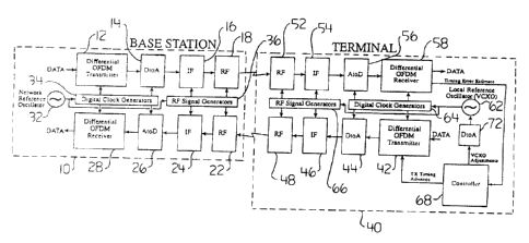
Referring to Fig. 1, a base station 10 includes
an OFDM transmitter 12, a digital to analog convertor 14,
and a radio section formed of IF and RF transmitters 16 and
18 for upconverting baseband signals. The base station 10
also includes a radio section including RF receiver 22, IF
downconvertor 24, analog to digital convertor 26 and OFDM
receiver 28. A network reference oscillator 32 supplies a
master reference frequency to digital clock generators 34
connected to the OFDM transmitter 12 and OFDM receiver 28,
and to RF signal generators 36 connected to the
downconvertors 22 and 24 and the upconvertors 16 and 18 in
the transmit and receive radio sections respectively.
A wireless: terminal 40 is used in conjunction
with the base station l0 and includes an OFDM transmitter
42, a digital to analog convertor 44, and a radio section
formed of IF and RF transmitters 46 and 48 for upconverting
baseband signals. The wireless terminal 40 also includes a
radio section for detecting RF OFDM signals including RF
receiver 52, IF downconvertor 54, analog to digital
convertor 56 (which may also be referred to as a sampler)
connected to receive downconverted signals from the IF
downconvertor 54 and OFDM receiver 58. A local voltage
controlled reference oscillator (VCXO) 62 supplies a
reference frequency to digital clock generators 64
CA 02347899 2001-06-12
connected to the OFDM transmitter 52 and OFDM receiver 58,
and to RF signal generators 66 connected to the
downconvertors 52 and 54 and the upconvertors 46 and 48 in
the transmit and receive radio sections respectively. The
5 digital clock. generators 64 are connected to receive a
reference frequency ,From the VCXO 62 and provide a digital
clock to the sampler 56 and OFDM receiver 58. The RF signal
generators 66 are .also connected to receive the same
reference frequency from the VCXO 62 and provide
intermediate RF signals to the radio sections comprised of
elements 46, 48, 52 and 54 for downconversion and
upconversion of the received and transmitted signals
respectively.
Still referring to Fig. 1, the OFDM receiver
computes a timing error estimate from received signals or
signal blocks supplied to it by the sampler 58 as described
below in relation to fig. 6A and supplies the timing error
estimate to a ron~troller 68. The controller 68, as
described in more detail in relation to Fig. 6A, supplies
a voltage, related t:o the timing error estimate, through
Digital to Analog convertor 72 to control the VCXO 62. The
timing error estimate may also be supplied by the
controller 68 to the OFDM transmitter 42 to advance timing
of signals transmitted by the wireless terminal 40.
All components in the base station 10 are
conventional. The R.F and IF sections, Atop convertors,
digital clock generators, RF signal generators, local
reference oscillator and differential OFDM transmitter in
the wireless terminal 40 may all be conventional elements.
Further description of an exemplary base station 10 and
wireless terminal that may be used in an embodiment of the
invention may be found in "Implementation of High
Performance Wireless LAN", McGibney et al, Proceedings,
CA 02347899 2001-06-12
6
Wireless 94, Calgary. Canada, 1994.
Since timing error measurements use the same OFDM
signals and receiver hardware that are used to carry
network data the system is kept simple. This eliminates
the overhead needed to send special timing signals and the
extra receiver hardware that would be required to process
those signals. The timing estimate is preferably based on
the constellation rotation property of differential OFDM
systems. The differential OFDM modulation scheme encodes
l0 data on frequency multiplexed subcarriers. If a subcarrier
at frequency fl has a phase of B~ and the next subcarrier at
frequency f~ + Of has a phase BZ then the information is
carried in the phase difference ~Z - B~. A shift in time of
e~ (where a positive ~~ represents a signal arriving late or
sampled early) causes the phase of each subcarrier to
change byy a value of -2nE~f (radians). The subcarriers are
then sampled with phases equal to B, - 2~re~, and 9z - 2~re~(f~
+ Of) respectively. When the phase differential is
evaluated to extract the data, the result is ~ BZ - 2~rts~ ( f~ +
Of)J -~ 91 - 2~rte~f,~ = B2 - B~ - 2~re~f. The result includes both
the data carrying phase difference (B2 - B~) and a constant
offset of -2~rs,~f (radians) caused by the timing error.
This derivation shows that an ideal OFDM signal
with subcarriers separated by Of Hz and arriving et seconds
late has its constellation rotated by -2~rOfe~ radians by
comparison with a pre-determined distribution of the phases
(typically 0°, 90°, 180° and 270°). For example,
if the
subcarrier spacing is 697kHz, the maximum timing error of
100ns rotates the constellation by 0.43rad (25 degrees).
The rotation required to rotate the constellation back to
the pre-determined distribution constitutes an estimate of
the timing error. Fic~. 2A shows an ideal OFDM constellation
CA 02347899 2001-06-12
7
without a timing error and Fig. 2B shows the same signal
with a timing error. The points in the constellation plots
are the complex value of each subcarrier multiplied by the
complex conjugate of the next lower subcarrier, therefore
the phase of each point in the plot represents a
differential phase between subcarriers. The timing error
estimate can be made by measuring the rotation of this
constellation from the ideal. By repeating the computation
of the rotation required, successive timing errors may be
computed, and use to adjust the reference oscillator 62.
Measurement of the timing error in a real
multipath environment is made more complex than the ideal
case since the received signal is composed of many
individual signals with different path delays. Fig. 2C
shows the constellation of an OFDM signal that has passed
through a multipath channel. The timing ambiguity results
in a different "group delay" for each subcarrier and
therefore the timing error estimate changes depending on
which subcarrier is observed. This problem is overcome by
defining a zero timing error as the point where the
constellation is rotated so that the individual subcarrier
timing errors are di~rtributed equally positive and negative
(Fig. 2D). This should ensure that the phase spread caused
by the multipath channel has a minimal effect on the phase
encoded data.
The procedure for estimating the timing error is
shown in Fig. 3. First, the data is estimated from the
phase and removed (for example, if the data pair O1 is
detected, the signal :is rotated by -90o to bring it in line
with data pair 00) . Then a vector average of all of the
subcarriers is computed. Finally, the phase of the vector
average is measured and converted into an equivalent timing
error. An efficient hardware implementation of this
CA 02347899 2001-06-12
8
algorithm is discussed below in relation to Figs. 6A and
6B.
The characteristics of this algorithm makes the
timing estimate very robust. The error estimate is based
on an average of hundreds of subcarriers so it remains
accurate even in low signal to noise ratio conditions. The
vector average weig'.hs the phase of smaller subcarriers
(which are more susceptible to channel noise, group delay
from the multipath channel, and data estimation errors)
less than larger subcarriers. When the differential phase
between subcarriez-s is computed using complex
multiplication, the <amplitude of the result is equal to the
product of the amplitude of the two subcarriers. If the
amplitude of either of the subcarriers is small, the
product is small and the result is not weighed strongly in
the average. And finally, the timing information is
extracted from the full bandwidth of the signal which
protects it from mult;ipath fading. Figure 4 shows the mean
and standard deviation of the timing estimate when
simulated with an AWGN channel and a measured multipath
channel with a 32.5n.s timing error. The estimate remains
stable down to an SNR of about IOdB (reliable data
transmission requires at least 20dB SNR).
Timing error corrections are made by making small
changes in the frequency of the terminal s reference
oscillator, which in turn controls the rate of the Atop
sample clock. Increasing the sampling clock by a ppm for
t seconds causes the sampling time to advance et
microseconds. If, f:or example, the receiver was sampling
50ns late, this could be corrected by increasing the
reference clock by l.ppm for 50ms.
The proportional feedback controller 68 shown in
Fig. 5A can be used to adjust the VCXO 62 to force timing
errors to zero. The timing error estimate, appearing as a
CA 02347899 2001-06-12
9
signal on line 69, ies amplified by a factor K, set equal to
-lppm/100ns in amplifier 70. In the diagram, e,represents
the timing error returned from the OFDM receiver in ns, and
v, is the VCXO offsets value in ppm. In this case, the
voltage supplied to the VCXO 62 is proportional to the
timing error. Normally timing measurements are made on the
same OFDM blocks that carry data from the base station 10
to the terminal 40. For terminals that are in an idle
state and not receiving a steady stream of data, the base
station 10 should provide an alternate block that these
terminals can share to maintain synchronization. This
block may also transport the system information needed to
wake up an idle terminal. If the signal was sampled late
(negative E,) then the feedback loop causes the VCXO 62 to
speed up until the sampling catches up with the signal.
Similarly, a signal sampled early causes the VCXO 62 to
slow down. The con~atant, K,, is set so that the maximum
allowable timing error (100ns) produces the maximum
allowable frequency offset (lppm) and therefore timing
adjustments do not violate the frequency offset tolerance.
The feedback loop described in the previous
paragraph works as long as there is no Lrequency o==sez
between the base station 10 and the terminal 40. Suppose
that the frequency of one of the reference oscillators
drifts 0.5 ppm away from the frequency of the other. When
the loop is synchronized, the output of the control loop
has to be -0.5 ppm t:o counter the effect of the frequency
offset, therefore a steady state timing error of 50 ns has
to be maintained. 7.f the frequencies drift apart by more
than lpprn then the proportional control loop could not keep
both the timing and ,Frequency offset within tolerance. The
problem of frequency drifting can be alleviated by adding
CA 02347899 2001-06-12
an integrator branch to the feedback loop as shown in Fig.
5H.
Referring t:o Fig. 5H, the controller 71 includes
the same amplifier 70 as in Fig. 5A. A feedback loop 73
5 after the amplifier 70 includes an amplifier Kz, whose value
is kept much less than 1, for example 0.01, a summer 74,
and a delay 76 on a delay loop after the summer 74. The
output of the feedback loop 73 is added to the output of
the amplifier 70 at summer 78. The effect of the delay is
10 to integrate the output from the amplifier KZ so that the
voltage supplied to t:he VCXO 62 includes a component that
is proportional to th,e timing error and a component that is
proportional to a sum of preceding timing errors.
Thus, the integrator loop detects the non-zero
condition at the input. of the feedback loop and adjusts its
output to compensate for the frequency offset. Frequency
drifting between the base statian 10 and terminal 40 is a
slow process usually caused by temperature drifts, supply
voltage changes, and component aging so the constant in the
integral loop can be set very small.
Even though the data rate of the network is very
high, timing adjustments can be made relatively slowly.
The proportional feedback loops in Fig. 5 sets the VCXO to
a value that corrects the measured timing error in 100ms.
To prevent overshoot, the timing should be readjusted
before it reaches the zero point, therefore the VCXO
frequency needs to bE: updated at a rate greater than lOHz.
Since terminals typically spend most of their time in an
idle state, minimizing the number of blocks that the
terminal must decode to maintain timing conserves battery
energy. A typical rate that satisfies both conditions is
20 timing adjustments per second. If the oscillators are
sufficiently stable, it would be possible for the terminals
CA 02347899 2001-06-12
11
to go into a low-power, standby mode where they would
reduce the feedback variable, K,, to slow down the speed of
the timing corrections so even fewer timing estimates are
required. It K, is reduced by too much however, the timing
conditions may change faster than the feedback loop can
respond and timing lock is lost.
When a tercininal first connects to the network, it
must contend with an arbitrary timing offset and a large
potential frequency offset (up to lOppm with realistic
crystals). Before the feedback loops of Figs. 5A and 5B
can be engaged, bath the timing and frequency offsets must
be, or be brought:, within tolerance. The signal
acquisition algorithm synchronizes to a block with a known
data pattern called the header block that is transmitted
periodically from th.e base station 10. The header block
uses the same OFDM format as all other blocks except that
all 400 of its bits are fixed and it does not contain any
parity bits. It also serves as a marker for the start of
a frame and as a power level reference. The terminal
performs a search fc~r this header block and, once found,
use it to calculate and remove the timing and frequency
offsets.
To aid in the search, the frequency off set
tolerance is preferably loosened, for example to 3ppm. The
higher bit error rate that results is tolerable since the
search algorithm need only to determine whether a signal is
the header block or not. All 400 bits of the header block
are known so the a7.gorithm can identify any block that
matches at least Borne pre-selected threshold number, for
example :i00, of these bits as the header block and provide
a signal indicative of positive detection if a match is
found. This almost certainly rejects anything but the
header block while properly identifying the header with a
CA 02347899 2001-06-12
12
bit error rate as high as 0.25. The probability of
randomly getting at least 300 bits correct out of 400 is
about 10'~ .
The search algorithm starts with a guess of the
frequency offset and searches for the header with the
assumption that the real offset is within lppm of the
guess. The reference oscillator 62 is set to a value 2ppm
higher than the guess which puts it between lppm and 3ppm
higher than the actual offset. This intentional offset
placed on the reference oscillator 62 causes the timing
error to change at a rate between i~s/s and 3~s/s. OFDM
blocks arrive at a rate of one block every 1.8~s so the
timing error crosses zero every 0.6s to 1.8s (depending on
the actual offset). As the OFDM blocks are sliding in and
out of proper timing synchronization, the OFDM receiver 58
decodes as many blocks as it can, looking for the header
block. At the fastest sliding .rate, the signal is within
the t100ns timing error range for 67ms, enough time to
process 37,000 blocks. If the base station 10 places one
header block every :1000 blocks, the search algorithm has
plenty of opportunityy to find the header block as it slides
by and the header blocks do not add any significant
overhead to the network. Once the header block is found,
then the system can monitor just that block until the
timing error reaches zero.
When the header block has been found and the
timing error removed, the frequency offset can be measured
and removed. This mr~asurement is made by first introducing
an intentional timing error by setting the reference
oscillator to an initial frequency offset, for example 2ppm
below the guess offset, for a fixed amount of time. During
this time, the terminal's receiver is not active. Then, the
measurement proceeds by setting the oscillator back to some
CA 02347899 2001-06-12
13
other frequency offset, for example 2 ppm above the guess,
activating the receiver, and measuring the time it takes
for the header block to return to proper timing. The
frequencies used should straddle the actual (but unknown)
frequency of the transmitted OFDM signal, with one above
and one below the actual frequency. If the actual frequency
offset differs from the guess, then the terminal slides
away from the proper timing point at a different rate than
it slides back. By measuring the time that it takes for
the timing error to return to zero, the actual frequency
offset can be calculated from the following equation:
~fo = Ofptp+~fptp
t"+tp
where
~fo is the corre~rt frequency offset.
~f" is the frequency offset used to introduce the
timing error
OfP is the frequency offset used to correct the timing
error
t" is the amount of time spent to introduce the timing
error.
tP is the measured time that it took to correct the
timing error.
Since the value sent to the DtoA converter 72
that controls the VC'XO 62 is directly proportional to the
frequency offset, the DtoA values may be used for Of" and
Ofp. The equation then returns the value that should be
sent to the DtoA converter 72 to get the correct offset.
Time measurements cam be made in any unit. A convenient
unit to base is the period between header blocks. In that
case the terminal need only count out a fixed number of
header blocks to introduce the taming error, then count the
CA 02347899 2001-06-12
14
number of header blocks that pass before the timing returns
to normal.
The system can then set the reference oscillator
62 to the calculated offset frequency and engage the
feedback loop 71 to maintain correct timing.
The timing error found using the header block
need not be set to 2:ero to find the frequency offset, but
some other pre-determined value may be used. However, a
zero timing error makes the computations somewhat easier.
If the ofi'set guess is not within lppm of the
actual offset then one of two things happens: either the
header is not found within 1.8s in the initial search, or
the signal does not return to zero timing error within a
time of 3t" during the frequency offset calculation. If
either of these conditions occur then a new offset guess
has to be made and the whole procedure repeated until the
full range of the reference oscillator 62 has been
explored. A good initial guess would be the frequency
offset when the terminal 40 last disconnected from a
network. If there have not been any drastic changes in the
environment, this value should be very close to the actual
offset. Subsequent guesses preferably radiate out from
that !for example, 2ppm above, 2ppm below, 4ppm above,
etc.) thus using subsequent frequency offsets that are
different from the first guess at the frequency offset.
The base ectation 10 of the network establishes
evenly spaced timir.,g slots where it can transmit and
receive .information. As described above, the terminal 40
times its receiver clocks 64 so that they receive the base
station s signals at the proper time and in this manner the
wireless terminal is synchronized to the base station. The
wireless terminal 40 should also time its transmitted
CA 02347899 2001-06-12
signals so that they arrive at the base station 10 at the
proper time.
One method that the terminal 40 could use would
be to tie its transmitter clock directly to its receiver
5 clock so it transmits at the same position within the slot
as it receives. This method will work until the two
devices move far enough apart that the propagation delay
between them becomes significant. The signal that the
base station 10 receives from the terminal 40 arrives two
10 propagation times late due to the round trip delay. In
order for the terminal' s signal to arrive at the proper
time at the base station 10, the terminal 40 must transmit
earlier in the timing frame than it receives.
When the terminal 40 first connects to the base
15 station 10 it assumes that the propagation delay is zero
and transmits a bloclK to the base station 10. The network
frame will be divided into two sections, the first is where
the base station 10 transmits to the terminal 40 and the
second is where the terminal 40 replies. In-between
sections will be one or two unused slots where the
transients from power amplifiers powering up and down are
allowed 1.o settle. When the terminal 40 first transmits
back to the base station 10, it should be assigned the last
time slot: in the frame. When the signal arrives late, it
will only interfere with an unused slot. In this manner,
the signal sent from the wireless terminal to the base
station is synchronized to the synchronization of the
receiver at the wireless terminal. The base station 10
measures the timing error created by the communication
channel according to the method of the invention and
transmits, through for example a digital control channel,
the result back to the terminal 40 where the transmit
timing can be adjusted. Note that at this point, the
timing error could be as much as 200ns (for a 30m
CA 02347899 2001-06-12
16
separation) which would prevent the base station 10 from
decoding the block. If this happens repeatedly, then the
base station 10 can ask the terminal 40 to transmit loons
earlier and then trot again. Once the proper transmitter
timing is achieved it should be checked and updated
periodically. In indoor applications, the distance between
devices does not change rapidly so the update frequency
should be on the order of once per second.
Fig. 6A eh.ows a preferred implementation of the
timing error estimation hardware. To simplify the process
of data estimation and removal, the timing of the signal is
advanced with timing adjustor BO before the OFDM
demodulator 82 to produce a 45° bias in the output
constellation. In F1ET based OFDM demodulators, the timing
advancement can be achieved by moving the beginning eighth
of the data set to the end of the data set before
performing the FFT. Since the FFT algorithm requires that
the data be re-ordered before processing, this operation
can be merged into the FFT operation in a way that does not
add any complexity to the circuit. With the 45o bias in
the constellation, creating an estimate of the data bit
pair from the subcarrier products becomes a trivial matter
as is shown in Fi.g. 6H. Any time that the signal falls
below the real axis, then the high order bit is one; or
equivalently, the high order bit is the sign bit of the
imaginary component of the signal. Similarly, the low
order bit is the sign bit of the real component.
The OFDM demodulator 82 repeatedly clocks out the
detected subcarrier measurements in order, for example from
the lowest frequency to the highest.
The subcarrier measurements (real and imaginary
values) are output from the OFDM demodulator 82 to a
computing means 84 that carries out a complex
multiplication of complex values X and complex values Y.
CA 02347899 2001-06-12
17
Such computing means are well known in the art. The values
X are received directly from the OFDM demodulator 82.
Values Y are first delayed at delay means 86, and the
imaginary components of values Y are inverted by inverter
88. By selection of the appropriate delay, that is, the
time taken for one measurement, the value at Y will be one
subcarrier lower than the subcarrier received at X. The
computing means 84 outputs the value XY, from which the
phase differential of the subcarriers may readily be
determined by known methods. The phase differential
corresponds to the angle of the vector formed by the real
and imaginary components of the value XY in the complex
plane.
In the next block, estimator 90, the data is
estimated by the sign of the real and imaginary components,
and output at 92. Data is then removed from the signal by
computing means 94.
Removing the data from the signal will move all
four states of the constellation to the 00 state at 450. If
R is the real component of the signal, I is the imaginary
component, and T is ~~he signal with the data removed, then
the algorithm to remove the data can be expressed as:
If the data bits are 00, then T = R + jI;
else if the data bits are 01, then T = (R + jI)*(-j)
- I -jR;
else if the data bits are 11, then T = (R + jI)* (-1)
- -R -jI;
else if the dat<~ bits are 10, then T = (R + jI)* j = -
I + jR.
With some manipulation the algorithm can be reduced to:
If the data bits are 00 or 11, then T = ~R~ + j~I~%
else if the data bits are O1 or 10, then T = ~ I ~ +
7~R
CA 02347899 2001-06-12
18
It is this method that is implemented in Fig. 6A to remove
the data. The data is input to exclusive or gate 96 which
controls multiplexers 98 and 100. The multiplexers 98 and
100 work as follows. If the output from the exclusive OR
gate is low, or zero, then the multiplexers will output the
value at the zero input. If the output from the exclusive
OR gate is high, or 1, then the multiplexers will output
the value at the one input. The absolute value of the
output of the multiplexers 98, 100 is then taken at 102 and
104.
Once the data is removed, a pair of accumulators
106 in means 108 area used to calculate the vector average
of all subcarrier products. Technically this is
calculating a summation not an average, but both operations
produce a result w~.th the same phase component so the
change will not affe~~t the timing estimate. The amplitude
of this summation provides a good approximation of the
total power of the received signal and can be used for
automatic gain control.
The vectc>x- average is converted into an
equivalent timing error by the OFDM receiver 58. The OFDM
receiver 58 can calculate the timing in one step by
searching through a table with pre-computed tangents for a
number of timing values within the timing range. For
example, if the t100ns timing error range is divided into
64 table entries, t:he controller could search for the
timing error within 3ne with only a six level binary
search. Such an operation performed 20 times a second
would place only a mp~nor load on a simple micro-controller
chip.
A person skilled in the art could make immaterial
modifications to they invention described in this patent
document without departing from the essence of the
CA 02347899 2001-06-12
19
invention that is intended to be covered by the scope of
the claims that follow.