Note: Descriptions are shown in the official language in which they were submitted.
CA 02348261 2001-04-24
DESCRIPTION
PROGRAM PRODUCT AND DATA PROCESSING SYSTEM
TECHNICAL FIELD
The present invention relates to a control program product described with
microcodes or the like, and a data processing system capable of executing the
control
program.
BACKGROUND OF INVENTION
Processors (data processing systems or LSIs) incorporating an operation
function
such as microprocessor (MPU) and digital signal processor (DSP) are known as
apparatuses
for conducting general-purpose processing and special digital data processing.
Architectural
factors that have significantly contributed to improved performance of these
processors
include pipelining technology, super-pipelining technology, super-scalar
technology, VLIW
technology, and addition of specialized data paths (special purpose
instructions). The
architectural elements further include branch prediction, register bank, cache
technology, and
the like.
In the VLIW technology, the data paths are configured in advance so as to
allow for
parallel execution, optimization is conducted so that a compiler improves the
parallel
execution and generates a proper VLIW instruction code. This technology adopts
an
extremely rational idea, eliminating the need for the circuitry for checking
the likelihood of
parallel execution of individual instructions as in the super-scalar.
Therefore, this technology
is considered to be extremely promising as means for realizing the hardware
for parallel
execution. However, given a processor for use in processing of an application
that requires
image processing or special data processing, the VLIW is not an optimal
solution either.
This is because, particularly in applications requiring continuous or
sequential processing
using the operation results, there is a limit in executing operations or data
processing while
holding the data in a general-purpose register as in VLIW. This problem is the
same in the
conventional pipeline technology.
On the other hand, it is well known from the past experiences that various
matrix
CA 02348261 2001-04-24
calculations, vector calculations and the like are conducted with higher
performance when
implemented in dedicated circuitry Therefore, in the most advanced technology
for
achieving the highest performance, the idea based on the VLIW becomes major
with the
various dedicated arithmetic circuits mounted according to the purpose of
applications.
However, the VLIW is the technology of improving the parallel-processing
execution efFiciency near a program counter. Therefore, the VLIW is not so
effective in,
e.g., executing two or more objects simultaneously or executing two or more
functions.
Moreover, mounting various dedicated arithmetic circuits increases the
hardware, also
reduces software flexibility.
The architecture of FPGA (Field Programmable Gate Arrays) is capable of
changing
connection between transistors and controlling dynamically to some degree,
therefore,
various dedicated arithmetic circuits may be implemented. However, in FPGA
based
architecture, it takes a long time for dynamically changing the hardware, and
some another
hardware for reducing that time is required. Therefore, it is difficult to
dynamically control
I 5 the hardware during execution of the application actually, and it dose not
become an
economical solution. It is possible to retain the reconfiguration information
of the FPGA in
a RAM of two faces or more for operating in the background so as to
dynamically change the
architecture in an apparently short time. However, in order to enable this
reconfiguration to
be conducted within several clocks, it is required to mount the RAM that
stores all of number
of combinations of information for reconfiguring the FPGA. This does not at
all essentially
solve the economical problem of a long reconfiguration time of the FPGA.
Moreover, the
original problem of the FPGA, i.e. poor AC characteristics at the practical
level, that comes
from the purpose of FPGA to efficiently implementing mapping in terms of the
gate of the
hardware, is not likely to be solved for the time being.
It is therefore an object of the present invention to provide a system, such
as a
program product, a data processing system capable of executing the program and
a control
method of the processing system, in the system, complicated data processings
are flexibly
executed at a high speed without using various dedicated circuits specific to
those data
processings originally. 1t is another object of the present invention to
provide a more
economical data processing system, a control method of the processing system
and a program
product, allowing for dynamic hardware control even during execution of an
application, and
CA 02348261 2001-04-24
capable of implementing the software-level flexibility at the hardware level
and of executing
various data processings at a high speed.
SUMMARY OF THE INVENTION
Therefore, the present invention provides a program product for controlling a
data
processing system including a plurality of processing units. The program
product or program
apparatus including a data flow designation instruction for designating input
and/or output
interfaces of at least one of the processing units independently of the time
or timing of
execution of the processing unit so as to define a data path configured by the
processing unit.
This program can be provided in a form recorded or stored on a recording
medium readable
with the data processing system, such as ROM or RAM. This program can
alternatively be
provided in a form embedded in a transmission medium capable of being
transmitted over a
computer network or another communication.
The present invention also provides the data processing system comprising a
plurality of processing units including changeable input and/or output
interfaces; a unit for
fetching the data flow designation instruction for designating the input
and/or output
interfaces of at least one of the processing units independently of the time
or timing of
execution of the processing unit; and a data flow designation unit for
decoding the data flow
designation instruction and setting the input and/or output interfaces of the
processing unit so
as to configure a data path from a plurality of the processing units. The
program product of
the present invention controls the processing system. Accordingly, the data
path formed
from a combination of a plurality of processing units is changed with the
program, so that
various data processings are executed with hardware, i.e., the data path or
data flow, that is
suitable for each of that various processings.
A method for controlling the data processing system according to the present
invention includes a step of fetching a data flow designation instruction that
designates the
input and/or output interfaces of at least one of the processing units
independent of the
processing execution timing of the processing unit; and a data flow
designation step of
decoding the data flow designation instruction and setting the input and/or
output interfaces
of the processing unit so as to configure some data path from a plurality of
the processing
units.
3
CA 02348261 2001-04-24
Conventionally, the only way to handle with a complicated data processing is
to
prepare dedicated circuitry and implement a special instruction for using the
circuitry, thereby
increasing the hardware costs. In contrast, in the system of the present
invention, such as
the program product, data processing system and control method thereof, the
interfaces of
the processing unit as an arithmetic/logic unit are described, making it
possible to introduce
the structure of pipeline control and data path control into an instruction
set, i.e., program
product. This allows various data processings to be described with the program
and
executed with suitable hardware, whereby the data processing system having
both the
software flexibility and high-speed performance using dedicated circuitry is
provided by this
invention. Moreover, these data paths can be implemented without discontinuing
execution
of a main processing or general-purpose processing, therefore, the hardware is
dynamic
reconfigured during execution of an application.
Moreover, the present invention provides means that is effective not only in
execution of parallel processing near a program counter, but also in
simultaneous
pseudo-execution of two or more objects and simultaneous pseudo-execution of
two or more
functions. In other words, in the conventional instruction set, two or more
processings
respectively based on remote program counters, such as data processings and
algorithm
executions having different contexts, cannot be activated simultaneously. In
contrast, in the
present invention, the data flows are appropriately designated with the data
flow designation
instructions, enabling the above processings to be performed regardless of the
program
counters.
Accordingly, with this instruction set, data path that seems to be effective
in
improvement in parallel processing performance from the application side can
be incorporated
previously from the software, so that the data path (data flow) thus
implemented is activated
from the software at the instruction level and as required. Since these data
paths are used
not only for the data processings corresponding to specific purpose, but also
for such a
purpose as for performing as a general state machine, the structure of this
invention has an
extremely high degree of freedom.
Moreover, the present invention enables a data path formed from a combination
of
the processing units to be changed by designating the interface of the
processing units
according to the data flow designation instruction. Accordingly, unlike the
architecture of
CA 02348261 2001-04-24
changing the connections between transistors like FPGA, the data paths are
defined by merely
switching the interfaces between the processing units having an appropriate
and/or specific
data processing function. Therefore, the hardware is reconfigured in a short
time.
Moreover, the data processing system of the present invention does not have
the architecture
requiring a general usage at the transistor level like FPGA, the mounting or
packaging density
is improved, whereby a compact, economical data processor such as system LSI
can be
provided. In addition, since the redundant structure is reduced, the
processing speed is
increased as well as the AC characteristic is improved.
Thus, in the program, data processing system and control method thereof
according
to the present invention, the instruction defining the interfaces of at least
one processing unit
included in the data processing system is recorded or described. Therefore,
data flows
become describable and the independency of the data paths is improved. As a
result, such
structures are readily provided that conducts the data flow designation while
executing
another instruction of the program, and even allows internal data path of the
data processing
system in the idle state to be lent for a more urgent processing that is being
executed in
another external data processor or another data processing system within the
same chip.
Moreover, it is desirable that content or function of processing in the
processing unit
capable of configuring data paths by combining thereof, is changeable or
variable according to
the data flow designation instruction. In other words, in the data flow
designation unit and
the data flow designation step, it is desirable that the content of processing
in the processing
unit is changeable or variable according to the data flow designation
instruction. This
enables improvement in flexibility of the data path formed from a combination
of the
processing units, whereby an increased number of data processings can be
conducted by the
data-flow-type process with reduced hardware resources, allowing for
improvement in
performance.
The FPGA architecture may be employed in individual processing units. As
described above, however, it takes a long time to dynamically change or
reconfigurate the
hardware, and also another hardware for reducing that time of reconfiguration
is required.
This makes it difficult to dynamically control the hardware within the
processing unit during
execution of an application. Should a plurality of ILAMs be provided with a
bank structure
for instantaneous switching, switching on the order of several to several tens
of units of
5
CA 02348261 2001-04-24
clocks would requires a considerable number of bank structures. Thus, it is
basically
required to make each of the macro cells within the FPGA programmable
independently and
to detectable the time or timing of switching for implementing a program-based
control
mechanism. However, the current FPGA architecture is not enough to deal with
such a
structure, and a new instruction control mechanism for designating switching
at an
appropriate timing is required.
Accordingly, in the present invention, it is desirable to employ as the
processing unit
a circuit unit including a specific internal data path(s). The processing
units having
somewhat compact data paths are prepared as templates and combinations of the
data paths
are designated so as to conduct the data-flow-type processing. In addition, a
part of the
internal data path of the processing unit is selected according to the data
flow designation
instruction so as to change the fiznction or content of processing performed
in the processing
unit. As a result, the hardware becomes more flexibly reconfigured in a short
time.
For example, a processing unit including at least one logic gate and the
internal data
paths) connecting the logic gate with the input/output interfaces makes it
possible to change
the processing content of the processing unit by changing the order of data to
be input/output
to the logic gate, changing connection between the logic gates or selecting
the logic gate, and
these changing and/or selecting are possible only selecting a part of the
internal data path that
is prepared in advance. Therefore, the content of processing in the processing
unit is varied
in a reduced or shorter time as compared to the FPGA that reconfigures the
circuitry are
possible in the transistor level. Moreover, the use of the internal data path
that is ready to
use some purpose previously reduces the number of redundant circuit elements
and increases
the area utilization efficiency of the transistors. Accordingly, the mounting
or packaging
density becomes high and economical processing system is provided. In the
system, the data
paths suitable for high-speed processings are provided and AC characteristics
of the system
become also excellent. Therefore, in the present invention, in the data flow
designation unit
and step are capable, it is desirable to select a part of the internal data
path of the processing
unit according to the data flow designation instruction.
It is also desirable that the data flow designation unit has a fixnction as a
scheduler
for managing the interface of the processing unit, in order to manage a
schedule retaining the
interface of each processing unit that is set based on the data flow
designation instruction.
H
CA 02348261 2001-04-24
For example, in the case where matrix calculation is performed only for a
fixed time and
filtering is conducted thereafter, the connection between the processing units
within the data
processing system are performed prior to execution of each processings and the
each
connection is kept using a time counter. Replacing the time counter with
another
comparison circuit or external event detector enables more complicated,
flexible scheduling to
be implemented.
Moreover, it is desirable that input and/or output interfaces of a processing
block
formed from a plurality of processing units are defined according to the data
flow designation
instruction. Since the interfaces in a plurality of processing units become
changeable or
reconfigurable with a single instruction, data paths associated with the
plurality of processing
units becomes changeable or reconfigurable with the single instruction.
Accordingly, in the
data flow designation unit, it is desirable that to change or configure the
input and/or output
interfaces in a processing block formed from a plurality of processing units,
according to the
data flow designation instruction.
It is more desirable to provide a memory storing a plurality of configuration
data
defining the input and/or output interfaces in the processing block, and, in
the data flow
designation unit or step, to change the input and/or output interfaces in the
processing block
by selecting one of the plurality of configuration data stored in the memory
according to the
data flow designation instruction. Since the configuration data is designated
with the data
flow designation instruction, changing of the interface of the plurality of
processing units is
controlled from the program without making the instruction itself redundant.
BRIEF DESCRIPTION OF THE DRAWINGS
Fig. 1 illustrates an instruction set including data flow designation
instruction of the
present invention
Fig. 2 illustrates in more detail a Y field of the instruction set of Fig. 1.
Fig. 3 illustrates one example using the instruction set of Fig. 1.
Fig. 4 illustrates how data are stored in a register by the instruction set of
Fig. 3.
Fig. 5 illustrates a data processing system for executing the instruction set
of the
present invention.
Fig. 6 illustrates a program executed with a conventional CPU or DSP.
CA 02348261 2003-05-05
Fig,. 7 illustrates a 1>rograin of the dat4~ pro~essi~a~, systc:rn according
to the present
invention.
Fig. $ illustrates compiled program c>fttre program of 1~'ig. '7 using
instn.rction sets of
the present invention.
Fig. 9 illustrates another p.-ogram ofthe data pro~~:essing system according
to the
present invention.
Fig. 10 illustrates data flows confi'rured l:ry the l~r~;~gram ofFig. 9.
Fig. 11 shows a difFerent example of~ the data pro~:ressirug system capable;
of
designating a data flow.
Figs. 12(a)-12(c) illustrate examples showing how the data path is changed by
the combinations of DPUs;
Fig. 13 shows the sc;hE:matic strucaure c>f a tur-th~;r di~er~nt data
processing system
capable of executing data ,processing according tG.r the in.>trlactic~n set of
the present invention.
Fig. 14(a) illustrates a processor having the DFZJ;
Fig. 14(b)-14(c) illustrate; template sections which communicate with the
processor of Fig.l4(a)
Fi';. I s illustrates one of~the templates.
DE:SCRIPTIOI~ OF ~f1-IE: PREF'1~:RREIa IiMBODIME:I1TT
Hereinafter, the present invention will be descril7e.d a sroore detail with
reference to
the drawings. Fig. 1 shows the structure c>r format of the instnrction set
(instruction format)
according to the present invention. The instruction set (instruct.ion set of
DAP~DNA) 1 (') in
the present invention includes two fields' a first field palled instruction
execution basic field (X
field) I 1 and a second field called instruction execution pre:pararion cycle
field (additional field
or Y field) 1 Z capable of improving ei~iciency of the subsequent instnaction
execution. The
instruction execution basic field (X field) 1 I specifies a data operation
such as
addition/subtraction, OR operation, A1~D c5peraticu~ arid comparison, as well
as the contents
of various other data processings such as branching, and designates a location
(destination)
where the operation result is tc> be stored. ?~lc'reover" in order to improve
the utilization
eiliciency ofthe instructicm length, t:he :~ field I I includes only
information ofthe instructions
for execution. On the other band, the additional field (~' field) I? is
capable of describing an
instruction or instructions (information) independent of the: exec:ution
instruction in the X field
I 1 of the same instruction set, and for example, is assigned for- the
information for execution
CA 02348261 2001-04-24
preparation cycle of the subsequent instruction.
The instruction set 10 will be described in more detail. The X field 11 has an
execution instruction field 15 describing the instruction operation or
execution instruction
(Execution ID) to a processing unit such as arithmetic/logic unit, a field
(type field) 16
indicating valid/invalid of the Y field 12 and the type of preparation
instruction (preparation
information) described in the Y field 12, and a field 17 showing a destination
register. As
described above, the description of the type field 16 is associated with the Y
field 12 and can
be defined independently of the descriptions of the other fields in the X
field 11.
In the Y field 12, the preparation information defined by the type field 16 is
described. The preparation information described in the Y field 12 are
information for
making an operation or other data processing ready for execution. Some
specific examples
thereof are shown in Fig. 2. First, it is noted again that the TYPE field 16
in the X field 11 is
for describing information independently or regardless of the information in
the execution
instruction field 15. In the Y field 12, it is possible to describe an address
information field
26 that describes an address ID (AlD) 21, and address information 22 which
intended use is
defined by A>D 21. This address information described in the Y field 12 is
used for reading
and writing between registers or buffers and memories (including register
files), and block
transferring like DMA becomes ready by the information in the Y field. It is
also possible to
describe the information such as an address indicating a branch destination
upon execution of
a branch instruction (fetch address) and a start address upon parallel
execution in the Y field
12 as address information.
In the Y field, it is also possible to describe information 23 that defines an
instruction
of a register type, e.g., defined immediate (imm) and/or information of
registers serving as
source registers for the arithmetic operation or another logic operation
instruction (including
MOVE, memory read/write, and the like). In other words, it is possible to use
the Y field 12
as a field 27 that defines sources for the subsequent execution instruction.
Furthermore, in the Y field 12, it is possible to describe data flow
designation
instruction or data flow designator 25 defines interfaces (source,
destination) and processing
content or fiznction and/or their combination of an arithmetic/logic unit
(ALU) or other data
processing unit, e.g., a template having data paths) being ready to use.
Namely, the Y field
12 is utilized as a field 28 for description for defining reconfigure data
paths to be pipelines
9
CA 02348261 2001-04-24
(data flows or data paths) for conducting a specific data processing. In the Y
field 12, it is
also possible to describe the data flow designator 25 for starting or
executing the data flow
and designator 25 for terminating the data flow. Accordingly, the data flows
provided with
reconfigurable data paths defined by the Y field I 2 enables execution of
processes
independently of a program counter for fetching a code from a code RAM.
It should be understood that the format of the instruction set as shown in
Figs. 1 and
2 is only one of examples of instruction set having two independent
instruction fields
according to the present invention, and the present invention is not limited
to the format
shown in Figs. 1 and 2. It is possible to provide another instruction set that
no instruction is
described (NOP is described) in the X or Y fields and only the X field I 1 or
Y field 12 is
effective actually. Another instruction set including mixedly a mnemonic
operand and the
data flow designator and the programs having such the instruction set are also
possible. The
programs having the data flow designation instructions described continuously
are also
possible. A specific example is not described below for clarity of description
of the
invention, however, a program product having the data flow designation
instruction,
regardless a form of description, and a recording medium recording such a
program are also
within the scope of the present invention.
Fig. 3 shows an example of the instruction set 10 of this invention. In the
number
j-1 instruction set 10, T(j-1 ), the type field 16 of the X field 1 I
indicates that 32-bit immediate
is described in the Y field 12 of the same instruction set. "#00001234H" is
recorded as
immediate in the Y field 12 of the instruction set T(j-1 ). In the following
number j
instruction set T(j), "MOVE" is described in the execution instruction field
15 of the X field
11, and register R3 is indicated in the destination field 17. Accordingly,
when this number j
instruction set T(j) is fetched, an ALU of a control unit stores, in the
register R3, the
immediate "#00001234H" defined in the preceding instruction set T(j-1 ).
Thus, in the instruction set I 0 of this embodiment (hereinafter, the number j
instruction set 10 is referred to as instruction set T(j)), preparation for
the execution
instruction described in the instruction set T(j) is made by means of the
preceding instruction
set T(j-1 ). Accordingly, the whole of processing to be executed by the ALU of
the control
unit cannot be known from the instruction set T(j) alone, but is uniquely
determined from the
two instruction sets T(j-1 ) and T(j). Moreover, in the execution instruction
field 15 of the
CA 02348261 2001-04-24
instruction set T(j-1), another execution instruction for another process
prepared by the Y
field 12 of the preceding instruction set is described independently of the Y
field 12 of the
instruction set T(j-1 ). Furthermore, in the type field 16 and Y field 12 of
the instruction set
T(j), another preparation information of another execution instruction
described in the
execution instruction field of the following instruction set is described.
In this embodiment, preparation information (preparation instruction) of the
execution instruction described in the X field l 1 of the instruction set T(j)
is described in the
Y field IZ ofthe immediately preceding instruction set T(j-1). In other words,
in this
example, latency of preparation instruction corresponds to one clock. However,
preparation
information may be described in another instruction set prior to the
immediately preceding
instruction set. For example, in a control program of the control unit having
a plurality of
ALUs, or for data flow control as described below, the preparation instruction
need not be
described in the immediately preceding instruction set. Provided that the
state (environment
or interface) of ALUs or the configuration of templates set by preparation
instructions are
held or kept until the instruction set having the execution instruction
corresponding to that
preparation instruction is fetched for execution, the preparation instruction
can be described
in the Y field 12 of the instruction set 10 that is preformed several
instructions cycle before
the instruction set 10 having the execution instruction corresponding to the
preparation
instruction.
Fig. 4 shows the state where a data item is stored according to the
instruction set of
Fig. 3 in a register file or memory that functions as registers. A processor
fetches the
number j-1 instruction set T(j-1), and the immediate "#00001234I-I" is latched
in a source
register DPO.R of the ALU of the processor according to the preparation
instruction in the Y
field 12 thereof. Then, the processor fetches the following number j
instruction set T(j), and
the immediate thus latched is stored in a buffer 29b in the execution cycle of
the execution
instruction "MOVE" in the X field 11. Thereafter, the data item in the buffer
29b is saved at
the address corresponding to the register R3 of the memory or the register
file 29a. Even if
the storage destination is not registers but memories, by the instruction set
10 of this
embodiment enables the data to be loaded or stored in the execution
instruction cycle by
conducting the process according to the preparation information prior to the
execution
instruction.
CA 02348261 2001-04-24
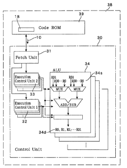
Fig. 5 shows the schematic structure of a processor (data processing system)
38
having a control unit 30 capable of executing a program having the instruction
sets 10 of this
embodiment. Microcodes or microprograms I 8 having the instruction sets 10 of
this
embodiment are saved in a code ROM 39. The control unit 30 includes a fetch
unit 31 for
fetching an instruction set 10 of the microprogram from the code ROM 39
according to a
program counter whenever necessary, and a first execution control unit 32
having a fianction
to decode the X field 11 of the fetched instruction set I 0 so as to determine
or assert the
fiznction of the ALU 34, and to select destination registers 34d so as to
latch the logic
operation result of the ALU 34 therein.
The control unit 30 further includes a second execution control unit 33 having
a
function to decode the Y field I 2 of the fetched instruction set 10 based on
the information in
the type field 16 of the X field 1 I and to select source registers 34s of the
arithmetic
processing unit (ALU) 34. This second execution control unit 33 is capable of
interpreting
the instruction or information in the Y field 12 independently of the
description of the X field
11, except for the information in the type field 16. if the information
described in the Y field
12 defines data flows, the second execution control unit 33 fiarther has a
function to select or
set the source and destination sides of the ALU 34, i.e., determine the
interface of the ALU
34, and to retain that state continuously until a predetermined clock or until
a cancel
instruction is given. Moreover, in the case where the information in the Y
field 12 defines .
data flows, the second execution control unit 33 fi~rther determines the
fi.~nction (processing
content) of the ALU 34 and retains that state for a predetermined period.
This control unit 30 fi~rther includes a plurality of combinations of such
execution
control units 32, 33 and ALUs 34, making it possible to execute various
processes. As a
result, a DSP for high-speed image data processing, a general CPU or MPU
capable of
high-speed digital processing, and the like, can be configured using the
control unit 30 as a
core or peripheral circuitry.
Figs. 6 to 9 show some sample programs executed by the control unit 30 of this
embodiment. A sample program 41 shown in Fig. 6 is an example created so as to
be
executable by a conventional CPU or DSP. This program extracts the maximum
value from
a table starting with an address #START and is terminated upon detection of
#END
indicating the last data.
12
CA 02348261 2001-04-24
A program 42 shown in Fig. 7 corresponds to the same procedure as that of Fig.
6,
the program is converted to the one suitable for the control unit 30 for
executing the
instruction sets of the present invention. The program 42 is generated for
executing two
instructions with a single instruction set. The program shown in Fig. 7 is
converted through
a compiler into an execution program of the instruction sets of the present
invention so as to
be executed by the control unit 30.
Fig. 8 shows the complied program 43. It is well understood in the programs 43
with reference to the program 42, preparation for the execution instructions
15 of the second
instruction set 10 is made in the Y field 12 of the first instruction set 10.
In the first
instruction set 10, the type field 16 indicates that immediate is described in
the Y field 12 as
preparation information. The second execution control unit 23 decodes the Y
field 12 and
provides the immediate to source caches or registers of the ALU 34. Therefore,
by the
second instruction set 10, the execution instructions 15 are executed on the
ALU 34 that has
been ready for those execution instructions. Namely, at the time when the
second
instruction set 10 is executed, to the registers defined in the destination
field 17, the
instructions of "MOVE" in the execution instruction field 15 are simply
executed.
Thus, according to the instruction set of the present invention, an execution
instruction can be separated from a preparation instruction that describes an
interface for
executing that execution instruction. Moreover, it is possible to perform the
preparation
instruction described in the instruction set that is fetched prior to the
execution instruction.
Therefore, according to the execution instruction described in each
instruction set, only the
execution corresponding to an arithmetic operation itself is simply executed,
because the data
has been read to the source side of the ALU 34. Accordingly, excellent AC
characteristics
and improved execution frequency characteristics is obtained. Moreover, like
the
conventional pipeline, although the times or timings of operations with
respect to the
execution instruction are different from that of the conventional pipeline,
operations such as
instruction fetching, register decoding, and other processings are performed
in a stepwise
manner. Thus, the throughput is also improved. In addition, the program of
this example
is capable of describing two instructions in a single instruction set.
Therefore, by parallel
execution of a plurality of instructions near the program counter like VLIW,
the processing
speed is further improved.
13
CA 02348261 2001-04-24
Moreover, in this program 43, conditional branching is described in the
execution
instruction field 15 of the fourth instruction set, and the address of subject
branch destination
is described in the Y field 12 of the preceding third instruction set.
Accordingly, the address
of the branch destination is set to the fetch register upon or before
execution of the fourth
instruction set. Thus, when the branch conditions are satisfied, the
instruction set at the
branch destination is fetched and/or executed without any penalty. It is also
possible to
pre-fetch the instruction at the brmch destination, so that preparation for
executing the
execution instruction at the branch destination can be made in advance.
Accordingly, even
the instruction at the branch destination is executed without loss of even one
clock. Thus,
the processing is accurately defined on a clock-by-clock basis.
Fig. 9 shows a program 44 of the present invention, which describes the data
flow
designation instructions 25 using the Y fields I 2 of the instruction sets 10.
A program
product 18 having such data flow designation instructions 25 is provided in
the form stored or
saved in the ROM 39, RAM, or another appropriate recording medium readable
with a data
processing system. Moreover, the program product 44 or 18 embedded in a
transmission
medium that is exchanged in a network environment may also be distributed.
Among the data tlow designation instructions 25 described in this program 44,
"DFLWI" is an instruction for initializing a data flow, and "DFLWC" is an
instruction
defining information of connections (information of interfaces) and processing
content
(fianction) of the arithmetic processing unit 34 forming the data flow (data
path). "DFLWT"
is an instruction defining the termination conditions of the data flow.
Instruction located the
end, "DFLWS" is for inputting data to the data flow thus defined and actuate
the processing
of the data path. These data flow designation instructions 25 are described in
the Y field 12
as preparation information and decoded by the second execution control unit
33, so that the
structures (configurations) for conducting the data processes are set by the
processing units
34.
Upon executing the program 44 shown in Fig. 9, the second execution control
unit
33 functions as a data flow designation unit according to the data flow
designation instruction
of the program, and the control according to the data flow designation step is
performed.
More specifically, the second execution control unit 33 decodes the data flow
designation
instruction 25 fetched by the fetch unit 31 and sets the input and/or output
interfaces of a
14
CA 02348261 2001-04-24
processing unit 34 independent of the time or timing of execution of that
processing unit 34.
In addition, depending on the data flow designation instruction 25, the second
execution
control unit 33 defines or changes the processing content of the processing
unit 34 as well.
Moreover, the second execution control unit 33 also functions as a scheduler
36 so as to
manage the schedule retaining the interfaces of each processing unit 34.
Accordingly, as shown in Fig. 10, the second execution control unit 33
functioning
as scheduler 36 defines the respective interfaces (input/output) and
processing contents or
fi~nctions of three arithmetic processing units 34, and retains that state or
configuration until
the termination conditions are satisfied. Accordingly, through the data flow
or data path
configured with these arithmetic processing units 34, the same process as that
shown in Fig. 6
proceeds in sequence independent of the program counter. In other words, by
designating
the data flow, dedicated circuitry for that process is provided in advance in
the control unit 30
by the three arithmetic processing units 34. Thus, the process of obtaining
the maximum
value is executed independent of the control of the program counter. The data
flow is
terminated if the ALU 34 functioning as DP1.SUB judges that DP1.R1 corresponds
to
#END.
Thus, as shown in Fig. 9, definition of the data flow enables the same process
as that
of the program shown in Fig. 6 or 7 to be executed without using any branch
instruction.
Accordingly, although the control unit 30 is a general-purpose control unit,
the control unit
30 can efficiently perform specific processes at an extremely high speed like
a control unit
having dedicated circuitry for each specific process.
Using the instruction set and the control unit according to the present
invention, it is
possible that data flows or pseudo data flows for various processings are
provided in the
control unit. Also, it is possible to apply these data flows, as templates, to
other processings
or programs. This means that, by software, the hardware becomes able to be
modified or
changed at any time to the configuration suitable for the specific data
processing, and the
resultant hardware configuration can be implemented also by other programs
and/or in other
hardware. It is also possible to set a plurality of such data flows, so that a
multi-command
stream can be defined in the control unit using software. This significantly
facilitates parallel
execution of a plurality of processings or processes, and it becomes possible
to arbitrarily
control their execution contents by programming.
CA 02348261 2001-04-24
Fig. 11 shows a different embodiment of the data processing system capable of
being controlled by the program 41 having the data flow designation
instructions 25. This
data processing system 40 is provided as a system LSI, and includes a code RAM
39 having
the program 41 recorded thereon, and a fetch unit 42 capable of fetching an
instruction from
the code RAM 39. The fetch unit 42 of this embodiment includes a data flow
decoder
(DFDEC) 42b for decoding a fetched data flow designation instruction 25, and a
decoder 42a
for decoding a general instruction other than the data flow designation
instructions 25.
Accordingly, the program 41 controlling this data processor 40 may include
both the data
flow designation instructions 25 and other general-purpose instructions.
Alternatively, a
program including the data flow designation instructions 25 and a program
formed from other
general-purpose instructions are provided in the code RAM 39 so that the
instructions from
these programs are fetched while synchronizing them by an appropriate method.
The general-purpose instruction is decoded by the general-purpose decoder 42a,
and the decode signal ~p is supplied for execution to an embedded general-
purpose processor
43 including ALUs, registers and the like. On the other hand, the data flow
designation
instruction 25 is decoded by the DFDEC 42b, and the decode signal ~f is
supplied to a data
flow processing unit (DFU) 45 for performing the instructions.
The DFU 45 of this embodiment comprises a plurality of data processing units
(DPU) 46. Each DPU 46 is a reconfigurable processing unit having data paths)
formed by
the respective FPGA. Accordingly, the DPU 46 includes an FPGA 46c, a RAM 46b
or
ROM having mappings of the FPGA 46c stored therein, an interface 46d for
controlling data
input/output to/from the FPGA 46c, and a configuration control portion 46a for
supplying the
mapping information and interface information stored in the RAM 46b to the
FPGA 46c and
interface 46d so as to define their configurations or states.
In this data processor 40, the fetch unit 42 conducts the step of fetching an
instruction set including the data flow designation instruction, and the DFDEC
42b functions
as the data flow designation unit and performs control process including the
data flow
designation step. In other words, the DFDEC 42b decodes the data flow
designation
instruction so as to designate the interface 46d of the DPU 46 through the
configuration
control portion 46a of each DPU 46 of the DFU 45. Accordingly, the data flow
designation
instruction 25 allows for control of the connection of the DPUs 46 in the DFU
45, so that
1H
CA 02348261 2001-04-24
data paths) formed from a plurality of DPUs 46 are configured and/or
controlled flexibly at
the program level.
In Fig. 12(a), two data paths 47a and 47b are configured from twelve DPUs 46.
In
contrast, by changing the interfaces of the DPUs 46, another single data path
48 capable of
executing another data process different from that of Fig. 12(a) is configured
from twelve
DPUs 46, as shown in Fig. I 2(b). Data paths configurable from a plurality of
DPUs 46 is
not limited to this, and three or more data paths are possibly defined in the
DFU 45 of the
data processor 40 by the software using the data flow designation
instructions. As a result,
parallel execution of a plurality of processes is significantly simplified.
Moreover, if any
DPU(s) 46 is available, another appropriate data path can be configured
therewith for use in
another data processor.
Moreover, the processing of combining the DPUs 46 to configure, reconfigure or
change the data path can be conducted without discontinuing the data
processing in another
data path, or without discontinuing the processing in the embedded processor
43. Moreover,
without changing of the processing in the FPGA 46c, dynamic changing of the
data path
becomes possible by merely changing the setting of the interface 46d.
Moreover, in the case
of changing the processing content of (processing itself in) the DPU 46, the
time required for
re-mapping is reduced by employing the FPGA 46c having a somewhat small
circuit scale.
Accordingly, a program can flexibly configure data paths corresponding to the
data processes
of the application to be processed by the data processing system 40, and that
data processes
are executed at an extremely high speed. In the current FPGA, however, the
hardware is
not enough to conduct mapping in several to several tens of clocks as
described above.
Therefore, in order to execute a desired data flow processing, instruction
thereof must be
made about several or several tens of clocks before the execution, thereby
increasing the
limitations like requirement for consistency with the start of the data
processing and with
branch instructions in describing the data flow designation instructions in
the program.
Fig. 13 is a schematic structure of a data processing system provided as a
system
LSI 50, having a plurality of processing units (templates) capable of defining
a data flow by
the instruction set 10 including the X field 11 and Y field I Z of this
invention. This system
LSI 50 includes a processor section S 1 for conducting data processings, a
code RAM 52
storing a program 18 for controlling the processings in the processor region
51, and a data
17
CA 02348261 2001-04-24
RAM 53 storing other control information or data of processing and the RAM 53
becomes a
temporal work memory. The processor section S 1 includes a fetch unit (FU) 55
for fetching
a program code, a general-purpose data processing unit (multi-purpose ALU,
first control
unit) 56 for conducting versatile processing, a data flow processing unit
(DFU, second
control unit) 57 capable of processing data in a data flow scheme.
The LSI 50 of this embodiment decodes the program code that includes a set of
X
field 11 and Y field 12 in the single instruction set 10 and executes the
processing accordingly.
The FU 55 includes a fetch register (FR(X)) 61x for storing instruction in the
X field 11 of
the fetched instruction set 10, and a fetch register (FR(Y)) 61y for storing
instruction in the Y
field 12 thereof The FU 55 fiarther includes an X decoder 62x for decoding the
instruction
latched in the FR(X) 61x, and a Y decoder 62y for decoding the instruction
latched in the
FR(Y) 61y. The FU 55 fizrther includes a register (PC) 63 for storing an
address ofthe
following instruction set according to the decode result of these decoders 62x
and 62y, and
the PC 63 fiznctions as a program counter. The subsequent instruction set is
fetched at any
time from a predetermined address of the program stored in the code RAM 52.
In this LSI S0, the X decoder 62x fianctions as the aforementioned first
execution
control unit 32 and the Y decoder 62y fianctions as the second execution
control unit 33, i.e.,
the data flow designation unit. Accordingly, the Y decoder 62y conducts the
data flow
designation step of the present invention of decoding the data flow
instruction described in
the Y field 12 of the instruction set 10, and based on the decoding, setting
the input/output
interfaces of the processing units of the DFU 57 so as to configure the
appropriate data path.
Thus, in the control method of the data processor 50 shown in Fig. 13, the
fetch unit 55
conducts the step of fetching a data flow designation instruction 25 that
designates the
inputJoutput interface of the processing unit independently of the time or
timing of execution
of that processing unit. The Y decoder 62y conducts the data flow designation
step of
decoding the data flow designation instruction 25 and setting the input and/or
output
interfaces of the processing units so as to configure the data path from a
plurality of
processing units.
The multi-purpose ALU 56 includes the arithmetic unit (ALU) 34 as described in
connection with Fig. 5 and a register group 35 for storing input/output data
of the ALU 34.
Provided that the instructions decoded in the FU SS are the execution
instruction and/or
18
CA 02348261 2003-05-05
preparation information ofthe: AL,L,~ ;34, a decode si,~;nal cpx oftlne ;~
decoder 62~: and a
decode signal ~y of the Y decoder Ei2y are ,,applied respectively to i:he
rrrulti-purpose ALLY 56,
so that the described processing is perfinzned in the AL I~ ~~~ as exlnlained
above.
The DFU 57 has a template s~ctic~n 7? where a p6urality of templates 7l for
configuring one of a plurality data flows or psevrdo data llc;,ws fear various
process>ings are
arranged. As described above in connection with >"'igs. 9 and 1 (), each
template 71 is the
processing unit (processing circuit) having a function as a S3peciiic data
path or data flow, such
as the arithmetic-processing unit (ALLl;I. lrVlrrrr the S' de~.ocler d~'y
decides the; dai:a flow
designation instructions 2,5 described as preparation ir~iar matit>n in the Y
field 1 ~, the
respective interfaces and corntents of function of processing in the templates
71, i.e., the
pr ocessing units of the DF1.1 _' %, are: set based c>n the sigrra~ ray
Accordingly, it is possible to c:han~;e the, respective c;or unr?.ctions of
the templates 71
and processes in that templates 71 by tyre dicta fl«r~= clesi~;:°~~rtor
25 described in the Y field 12.
Thus, with Combination of these templates 7I, data path(,s~ ~:uitable for the
specific data
processing is flexibly configured in the template region 7'wby means of the
data flow
designator included in the pro~~;uam 18. 'Cirus, dedicated r;ircuitry(s) for
the specific.
processing is provided in the proce.,sor 51, whereby the processin ~; therein
is conducted
independently of the control r~fthe program counter Irr r~ttver words, since;
the data flow
designation instructions ~'S are able tc~ change the respective inputs/outputs
of the templates
71 and processes in the templates 71 by software, the lra:rdware ofthe
pracessor 51 is
modified or reconfigured at any time to the confrguration suitable fbr the
speci~icr data
processing.
Figs. 14(a)-14(0) show the state whore different dedicated circuits titre
formed
with different combinations of templates. As shown i.rr Fib;. 14(a), in order
to perform
some process on the input data din i:o getting the output data gout by the DFU
57 of this
processor ~1, it is possible to set the respective interfaces of the templates
'?1 by the
data flow designator 25 so that tlae data processing is performed with the
templates 1-l,
1-2 and 1-:3 being connected in series with each other as shown in Fig. 14(b).
Similarly,
for the other templates 71 ire the template block 72, it is possible to set
their- respective
interfaces so as to configure data paths or data flows with appropriate
combinations of a
plurality of templates 7 1. Thus, a plurality oi' dedicated or special
processing units or
dedicated data paths 7:3 that are suitable for processing the input: data din
are configured
at any time in the template section 7 2 by rrreans of the program 18.
~.9
CA 02348261 2001-04-24
On the other hand, in the case where the process for performing on the input
data
din is changed, it is possible to change the connection between the templates
71 by the data
flow designation instructions 25, as shown in Fig. 14(c). The Y decoder 62y
decodes the
data flow designation instructions 25 so as to change the respective
interfaces of the
corresponding templates 71. Such control process (data flow designating step)
of the Y
decoder 62y enables one or a plurality of data paths 73 suitable for executing
another
different processings to be configured in the template section 72 with the
templates I-I, 2-n
and m-n being connected in series with each other.
These templates 71 are not limited to be combined as shown in Fig. 14, but may
also
I 0 be combined as shown in Fig. 12. The single processing unit formed from a
single template
71 or combination of a plurality of templates 71 can also be assigned to
another processing or
another program that is executed in parallel. In the case where a plurality of
processors 51
are connected to each other through an appropriate bus, it is also possible to
configure a train
(data path) 73 having the templates 71 combined for a data processes that is
mainly
performed by another processor 51, thereby making it possible to make use of
the data
processing resources, i.e., the templates 71, extremely effectively.
Moreover, unlike the FPGA intended to cover even implementation of a simple
logic gate such as "AND" and "OR", the template 71 of the present invention is
a higher-level
data processing unit including therein some specific data path which basically
has a function
as ALU or other logic gates. The respective interfaces of the templates 71 are
defined or
redefined by the data flow designation instructions 25 so as to change the
combination of the
templates 71. Thus, a larger data path suitable for desired specific
processing is configured.
At the same time, the processing content or processing itself performed in the
templates 71
can also be defined by the data flow designation instructions 25 changing the
connection of
the ALU or other logic gates or the like within the template 71. Namely, the
processing
content performed in the templates 71 are also defined and varied by selecting
a part of the
internal data path in the template 7 I .
Accordingly, in the case where the hardware of the DFU 57 having a plurality
of
templates 71 of this example arranged therein is reconfigured for the specific
data processing,
re-mapping of the entire chip as in the FPGA or even re-mapping on the basis
of a limited
logic block is not necessary. Instead, by switching the data paths previously
provided in the
CA 02348261 2001-04-24
templates 71 or in the template section 72, or by selecting a part of the data
paths, the desired
data paths are implemented using the ALUs or logic gates prepared in advance.
In other
words, within the template 71, connections of the logic gates are only reset
or reconfigured
within a minimum requirement, and even between the templates 71, the
connections are only
reset or reconfigured within a minimum required range. This enables the
hardware to be
changed to the configuration suitable for the specific data processing in a
very short or limited
time, in units of clock.
Since FPGA incorporates no logic gate, they are extremely versatile. However,
FPGA include a large number of wirings that are unnecessary to form logic
circuitry for
implementing fi.~nctions of a specific application, and such redundancy
hinders reduction in
length of signal paths. FPGA occupies a larger area than that of an ASIC that
is specific to
the application to be executed, and also have degraded AC characteristics. In
contrast, the
processor 51 employing the templates 71 of this embodiment which incorporate
appropriate
logic gates in advance is capable of preventing a huge wastefial area from
being produced as
in the FPGA, and also capable of improving the AC characteristics.
Accordingly, the data
processing unit 57 in this embodiment based on the templates 71 is a
reconfigurable processor
capable of changing the hardware by means of a program. Thus, in this
invention, it is
possible to provide the data processing system having both a higher-level
flexibility of
software and higher-speed performance of hardware compared to a processor
employing
FPGAs.
Appropriate logic gates are incorporated in these templates 71 previously,
therefore,
the logic gates required for performing the specific application are
implemented at an
appropriate density. Accordingly, the data processing unit using the templates
71 is
economical. In the case where the data processor is formed from FPGA, frequent
downloading of a program for reconfiguring the logic must be considered in
order to
compensate for reduction in packaging density. The time required for such
downloading
also reduces the processing speed. In contrast, since the processor S 1 using
the templates
71 has a high packaging density, the necessity of compensating for reduction
the density is
reduced, and frequent reconfiguration of the hardware is less required.
Moreover,
reconfigurations of the hardware are controlled in the units of clock. In
these respects, it is
possible to provide a compact, high-speed data processing system capable of
reconfiguring
21
CA 02348261 2001-04-24
the hardware by means of software that is different from the FPGA-based
reconfigurable
processor.
Moreover, the DFU 57 shown in Fig. 13 includes a configuration register (CREG)
75 capable of collectively defining or setting the respective interfaces and
content of
processings (hereinafter referred to as configuration data) of the templates
71 arranged in the
template section 72, and a configuration RAM (CRAM) 76 storing a plurality of
configuration data Ci (hereinafter, i represents an appropriate integer) to be
set to the CREG
75. An instruction like "DFSET Ci" is provided as an instruction of the data
flow
designators 25. When the Y decoder 62y decodes this instruction, desired
configuration
data among the configuration data Ci stored in the CRAM 76 is loaded into the
CREG 75.
As a result, configurations of the plurality of templates 71 arranged in the
template section 72
are changed collectively. Alternatively, configuration may be changed on the
basis of a
processing block formed from a plurality of templates 71.
It is also possible to set or change the configuration of the individual
template 71
when the Y decoder 62y decodes the data flow designation instruction 25 such
as DFLWI or
DFLWC explained above. In addition, as mentioned above, since the DFU 57 is
capable of
changing, with a single instruction, the configurations of a plurality of
templates 71 that
requires a large amount of information, the instruction efficiency is improved
as well as the
time expended for reconfiguration is reduced.
The DFU 57 fiarther includes a controller 77 for downloading the configuration
data
into the CRAM 76 on a block-by-block basis. In addition, "DFLOAD BCi" is
provided as
an instruction of the data flow designator 25. When the Y decoder 62y decodes
this
instruction, a number of configuration data Ci for the ongoing processing or
the processing
that would occur in the future are previously downloaded into the
configuration memory, i.e.,
the CRAM 76, among a large number of configuration data 78 prepared in advance
in the
data RAM 53 or the like. By this structure, a small-capacity and high-speed
associative
memory or the like is able to be applied as the CRAM 76 and the hardware
becomes
reconfigured flexibly and further quickly.
Fig. 15 shows an example of the template 71. This template 71 is capable of
exchanging the data with another template 71 through a data flow RAM (DFRAM)
79
prepared in the DFU 57. The processing result of another template 71 is input
through an
22
CA 02348261 2001-04-24
I/O interface 81 to input caches 82a to 82d, and then are processed and output
to output
caches 83a to 83d. This template 71 has a data path 88 capable of performing
the following
processing on data A, B, C and D respectively stored in the input caches 82a
to 82d, and of
storing the operation result in the output cache 83b and storing the
comparison result in the
output cache 83c. The processing result of the template 71 is again output to
another
template through the I/O interface 81 and DFRAM 79.
IFA==?
THEN (C+B) ==D
ELSE (C-B) ==D ~ ~ ~ (A)
This template 71 has its own configuration register 84. The data stored in the
register 84, in this template 71, controls a plurality of selectors 89 so as
to select a signal to be
input to the logic gates such as control portion 85, adder 86 and comparator
87.
Accordingly, by changing the data in the configuration register 84, in the
template 71, another
processing using a part of the data path 88 is possible to proceed. For
example, in the
template 71, the following processing is also provided without using the
control portion 85.
(B+C) ==D
(B-C) ==D . . . (g)
Similarly, by changing the data in the configuration register 84, a part of
the data
path 88 can be used so that the template 71 is utilized as a condition
determination circuit
using the control portion 85, an addition/subtraction circuit using the adder
86, or a
comparison circuit using the comparator 87. These logic gates are formed from
dedicated
circuitry that is incorporated in the template 71, therefore there is no
wastefial parts in terms
of the circuit structure and the processing time. In addition, it is possible
to change the input
and output data configurations to/from the template 71 by the interface 81
that is controlled
by the configuration register 84. Thus, the template 71 becomes all or a part
of the data
flow for performing the desired data processing.
This template 71 is also capable of rewriting the data in its own
configuration
register 84, based on either one of the data from the aforementioned CREG 75
and the data
from the Y decoder (YDEC) 62y of the FU 55 fimctioning as data flow
designation unit, and
selection thereof is controlled by a signal from the Y decoder 62y. Namely,
configuration of
this template 71 is controlled by the Y decoder 62y or the data flow
designation step
23
CA 02348261 2001-04-24
performed in the Y decoder 62y according to the data flow designation
instructions 25.
Therefore, both reconfiguration of hardware are possible, the one is to change
the hardware
configuration of the template 71, based on the DFSET instruction or the like,
together with
another templates) according to the configuration data Ci stored in the CRAM
76; and
another is to select a part of the specific data path 88 of the template 71 by
the data in the
configuration register 84 set by the data flow designation instruction 25.
Accordingly, configuration of the templates 71 is changed by the data flow
designation instructions 25 either individually or in groups or blocks,
whereby the data path of
the processor 51 is flexibly reconfigured.
The structure of the template 71 is not limited to the above embodiment. It is
possible to provide appropriate types and number of templates having logic
gates for
combining, selecting a part of inner data-path, and changing the combination
of the templates
71 for performing a multiplicity of data processings. More specifically, in
the present
invention, somewhat compact data paths are provided as several types of
templates. Thus,
by designating combination of the data paths, the data-flow-type processings
are implemented
thereby the specific processings are performed in an improved performance
condition. In
addition, any processing that cannot be handled with the templates is
performed with the
fianctions of the multi-purpose ALU 56 of the processor 51. Moreover, in the
multi-purpose
ALU 56 of this processor, the penalty generated upon branching and others, is
minimize by
the preparation instructions described in the Y field 12 of the instruction
set 10. Therefore,
the system LSl 50 incorporating the processor S 1 of this embodiment makes it
possible to
provide a high-performance LSI capable of changing the hardware as flexibly as
describing
the processing by programs, and it is suitable for high-speed and real-time
processing. This
LSI also flexibly deals with a change in application, specification without
reduction in
processing performance resulting from the change in specification.
In the case where the summary of the application to be executed with this
system
LSI 50 is known at the time of developing or designing the system LSI 50, it
is possible to
configure the template section 72 mainly with the templates having
configuration suitable for
the processing of that application. As a result, an increased number of data
processings can
be performed with the data-flow-type processing, thereby improving the
processing
performance. In the case where a general-purpose LSI is provided by the system
LSI 50, it
2~1
CA 02348261 2001-04-24
is possible to configure the template section 72 mainly with the templates
suitable for the
processing that often occurs in a general-purpose application such as floating-
point operation,
multiplication and division, image processing or the like.
Thus, the instruction set and the data processing system according to the
present
invention make it possible to provide an LSI having a data flow or pseudo data
flow
performing various processings, and by using a software, the hardware for
executing the data
flow can be changed at any time to the configuration suitable for a specific
data processing.
Moreover, the aforementioned architecture for conducting the data-flow-type
processing by
combination of the templates, i.e., the DFU 52 or template region 72, can be
incorporated
into the control unit or the data processing system such as processor
independently of the
instruction set 10 having the X field 11 and Y field 12. Thus, it is possible
to provide a data
processing system capable of conducting the processing at a higher speed,
changing the
hardware in a shorter time, and also having better AC characteristics, as
compared to the
FPGA.
It is also possible to configure a system LSI that incorporates the DFU 57 or
template region 72 together with a conventional general-purpose embedded
processor, i.e., a
processor operating with mnemonic codes. In this case, any processing that
cannot be
handled with the templates 71 may be conducted with the general-purpose
processor. As
described above, however, the conventional processor has the problems such as
branching
penalty and wasting of clocks for preparation of registers for arithmetic
processing.
Accordingly, it is desirable to apply the processor 51 of this embodiment
capable of decoding
the instruction set 10 having the X and Y fields for execution.
Moreover, with the processor 51 and instruction set 10 of this embodiment,
configurations of the DFU 57 are set or changed before execution of the data
processing, in
parallel with another processing by the Y field 12. This is advantageous in
terms of
processing efFrciency and program efficiency. The program efficiency is also
improved by
describing a conventional mnemonic instruction code and data-flow-type
instruction code into
a single instruction set. The fi.~nction of the Y field 12 of the instruction
set 10 of this
embodiment is not limited to describing the data-flow-type instruction code as
explained
above.
The processor according to the present invention is capable of changing
physical
_.,..m,"""". ~.. ,.. . .vl..s..,x.u~.fi ..
CA 02348261 2001-04-24
data path configuration or structure by the Y field 12 prior to execution. In
contrast, in the
conventional processor, a plurality of multiprocessors are connected to each
other only
through a shared memory. Therefore, even if there is a processor in the idle
state, the
internal data processing unit of that processor cannot be utilized from the
outside. In the
data processor according to the present invention, setting an appropriate data
flow enables an
unused hardware in the processor to be used by another control unit or data
processor.
As secondary effects, in the control unit of the present invention and the
processor
using the same, efficiency of the instruction execution sequence is improved,
as well as
independence and improved degree of freedom (availability) of the internal
data path is
ensured, therefore, the processings are successively executed as long as the
executing
hardware are available, even if instruction sequences for the processings
having contexts of
completely different properties are simultaneously supplied.
Now, the advantages of the cooperative design of hardware and software becomes
point out flourishingly, and the combination of the instruction set and the
control unit of the
present invention becomes an answer to the question how algorithms and/or data
processes
requested by the user are implemented in ei~cient and economical manner within
the
allowable hardware costs. For example, based on both the data and/or
information relating
to the instruction set of the present invention (the former DAP/DNA)
reflecting
configurations of the data paths those are already implemented, and to the
hardware and/or
sequence subsequently added for executing the process, new type of combination
that is
corresponding to the new data path (data flow) described with software,
becomes most
optimal solutions for the process and contributes for improving performance
are led while
minimizing the hardware costs.
In the conventional hardware, configuration is less likely to be divided into
elements.
Therefore, there is no flexibility in combination of the elements, and
basically, the major
solution for improving performance is to add a single new data path.
Therefore, the
conventional architecture is hard to evaluate numerically either in terms of
accumulating some
information for improving performance or of adding hardware information
actually
implemented for realizing the required improved performance, thereby making it
difficult to
create a database. In contrast, according to the present invention, since
compact data paths
are provided as templates and combination of the data paths is designated so
as to conduct
26
CA 02348261 2001-04-24
the data-flow-type processing, cooperation between hardware and software
becomes easily
estimated in an extremely meticulous manner for improving performance. It is
also possible
to accumulate trade-off information between hardware and software, therefore,
possibility of
the combination of data paths may be connected closely with the degree of
contribution to the
processing performance. This makes it possible to accumulate estimation data
relating to the
cost, the performance for required processes, and performance for execution
those are closely
relating to both hardware and software. In addition, since the data paths are
implemented
without discontinuing execution of the main processing or general-purpose
processing,
expected result to the addition for the performance request is predicted from
the accumulated
past data of the hardware and instruction sets of the present invention.
Therefore, the present invention contributes not only to significant reduction
in
current design and specification costs, but also to completing the next new
design with the
minimum trade-offbetween new hardware and software to be added. Moreover,
corresponding to the processing type, lending an internal data path to the
outside is facilitated,
therefore hardware resource sharing becomes possible. Accordingly, parallel
processing by
a plurality of modules of the present invention (DAPlDNA modules) becomes one
of the
most usefi~l aspects for implementing compact hardware.
Note that the aforementioned data processing system and instruction set are
one of
the embodiments of this invention, such that, in the data processor, it is
also possible to use an
external RAM or ROM instead of the code RAM or data RAM or the like, and to
additionally provide an interface with an external DRAM or SRAM or the like.
The data
processors additionally having known fianctions as a data processor such as
system LSI, e.g.,
an I/O interface for connection with another external device, are also
included in the scope of
the present invention. Accordingly, the present invention is understood and
appreciated by
the terms of the claims below, and all modifications covered by the claims
below fall within
the scope of the invention.
As has been described above, the present invention allows data paths) to be
flexibly
rearranged according to programs) by changing the respective interfaces of a
plurality of
processing units according to the data flow designation instructions. This
makes it possible
to flexibly execute individual complicated data processes with the hardware at
a high speed
without having various dedicated circuits specifically fixed to the respective
data processes.
27
CA 02348261 2001-04-24
Moreover, by employing as processing units the templates provided with a
specific data path,
according to the present invention, data paths (data flows) capable of
contributing to
improved performance can be accumulated with the resources, i.e., the
templates and the
instruction sets for utilizing the templates. Then, the accumulated data paths
become
possible to be updated at any time based on subsequently added hardware
configuration
information and sequence information for pertorming the data processing, so
that the optimal
solution is easily obtained. Accordingly, by the present invention, resource
sharing between
applications, resource sharing in hardware and investment of hardware for
improving
performance, those are conventional pointed out, will be proceeded in more
desirable manner,
and this invention will be significantly contributable as technology
infrastructure for
constructing networked society.
INDUSTRIAL APPLICABILITY
The data processing system of the present invention is provided as a
processor, LSI
or the like capable of executing various data processings, and is applicable
not only to the
integrated circuits of electronic devices, but also to the optical devices,
and even to the optical
integrated circuit devices integrating electronic and optical devices. In
particular, a control
program including the instruction set of the present invention and data
processor are capable
of flexibly executing the data processing at a high speed, and are preferable
for the processes
required to have high-speed performance and real-time performance like the
network
processing and image processing.
28
_~. ,..~ . ..,