Note: Descriptions are shown in the official language in which they were submitted.
CA 02348668 2001-04-23
WO 00/34964 PCTfAU99f01081
TITLE: A CHARGE STORAGE DEVICE
BACKGROUND OF THE INVENTION
The present invention relates to a charge storage device and a method of
manufacture thereof.
The inveni~on has been developed primarily for use with the electrochemical
charge storage devices such as supercapacitors and will be described
hereinafter with
reference to that application. It will be appreciated that supercapacitors are
designated
by terms such as ultra capacitors, electric double layer capacitors and
electrochemical
capacitors, amongst others, all of which are included within the term
"supercapacitor"
lo~ as used within this specification.
It is known to mass produce supercapacitors that have specific operational
characteristics that fall within well defined ranges. Although mass production
is
advantageous from a cost point of view, there is an inherent lack of
flexibility. That
is, if the desired characteristics of a supercapacitor for a particular
application fall
15 outside the commonly available ranges a compromise solution is required. An
alternative is to produce the desired supercapacitor as a one off or small
run. The
costs of this latter alternative are often prohibitive and, as such, rarely
pursued.
Known supercapacitors generally find application in power supplies such as
uninterruptible power supplies for computers or backup power supplies for
volatile
2o memory. Accordingly, it has been common to optimise these supercapacitors
for high
energy density, low self discharge rates, and low cost.
More recently it has been thought that supercapacitors are theoretically
applicable to high power pulsed applications. Indeed, some attempts have been
made
CA 02348668 2001-04-23
WO 00/34964 PCT/AU99/01081
-2-
to adapt such supercapacitors as short term current sources or sinks. Examples
of such
applications include internal combustion engine starting, load power leveling
for
hybrid vehicles and a variety of pulsed communication systems. However, the
success
of these supercapacitors has been limited by factors such as a high equivalent
series
resistance, among others. For example, some prior art double layer capacitors
make
use of button cell or spiral wound technology. These, in turn, fall generally
in one of
two groups, the first group being concerned with high power applications and
the
second with low power applications. For the second group, but not the first,
it has
been possible to obtain high energy densities.
l) The first and second groups are broadly defined by the type of electrolyte
used,
those being aqueous and non-aqueous respectively. This is predominantly due to
the
lower resistance inherently offered by aqueous electrolytes which makes it
better
suited to high power, and hence high current, applications. That is, the low
resistance
results in lower hR losses for aqueous electrolytes. The trade off; however,
is that for
l:i these aqueous electrolytes the voltage that can be applied across a
capacitive cell is
extremely limited.
The second group of prior art double layer capacitors suffers the converse
disadvantages. That is, while they provide a greater voltage window, which
improves
the available energy density, they also have had high internal resistances
which make
2o them unsuitable to the high power applications.
SIfMMARY OF TTHEE INVENTION
CA 02348668 2001-04-23
WO 00/34964 PCT/AU99/01081
-3-
It is an object of the present invention, at least in the preferred
embodiments, to
overcome or substantially ameliorate one or more of the disadvantages of the
prior art,
or at least to provide a useful alternative.
According to a first aspect of the invention there is provided a charge
storage
device including:
a first electrode;
a second electrode being opposed to and spaced apart from the first electrode;
a porous separator disposed between the electrodes;
a sealed package for contaning the electrodes, the separator and an
electrolyte
lt) in which the electrodes are immersed; and
a first terminal and a second terminal being electrically connected to the
first
electrode and the second electrode respectively and both extending from the
package
to allow external electrical connection to the respective electrodes, wherein
the
gravimetric FOM of the device is greater than about 2.1 Watts/gram.
15 Preferably, the gravimetric FOM of the device is greater than about 2.5
Watts/gram. More preferably, the gravimetric FOM of the device is greater than
about
3 Watts/gram. Even more preferably, the gravimetric FOM of the device is
greater
than about 3.5 Watts/gram. In some embodiments, the gravimetric FOM of the
device
is greater than about 5 Watts/gram.
2o More preferably, the first electrode and the second electrode form a
capacitive
cell and the device includes a plw~ality of the cells electrically connected
in parallel
and disposed within the package. In other embodiments, however, the cells are
connected in series. In still further embodiments a combination of series and
parallel
CA 02348668 2001-04-23
PCT/AU99/01081
-4-
connects are utilised. It will be appreciated that series connections allow
the cells to
be applied to higher voltage applications, while parallel connections allow
the cells to
provide a higher combined capacitance for the device. The ease at which these
different connections are accommodated by the invention means that prefer ed
embodiments are applicable to a wide variety of tasks ranging from high power
systems to low power systems.
In a preferred form, the maximum operating voltage of the or each capacitive
cell is less than about 4 Volts. More preferably, the maximum operating
voltage of
the or each capacitive cell is less than about 3.5 Volts. Even more
preferably, the
maximum operating voltage of the; or each capacitive cell is less than about 3
Volts
Preferably, the first electrode and the second electrode include a first
carbon
coating and a second carbon coatvig respectively wherein the surface area of
carbon
used in the coatings is greater than 20 m2/gram.
According to a second aspc;ct of the invention there is provided a method of
manufacturing a charge storage device, the method including the steps of
providing a first electrode;
disposing a. second electrode in opposition to and spaced apart from the first
electrode;
disposing a porous separator between the electrodes;
Zo containing within a sealed package the electrodes, the separator and an
electrolyte, wherein the electrodes are immersed in the electrolyte; and
electrically connecting a first terminal and a second terminal to the first
electrode and the second electrode respectively such that the terminals
extending from
CA 02348668 2001-04-23
WO 00/34964 PCT/AU99/01081
-S-
the package to allow external elecarical connection to the respective
electrodes,
wherein the gravimetric FOM of ithe device is greater than about 2.1
Watts/gram.
Preferably, the gravimetric FOM of the device is greater than about 2.5
Watts/grarn. More preferably, thf; gravimetric FOM of the device is greater
than about
3 Watts/gram. Even more preferably, the gravimetric FOM of the device is
greater
than about 3.5 Watts/gram. In some embodiments, the gravimetric FOM of the
device
is greater than abaut 5 Watts/gram.
More preferably, the first electrode and the second electrode form a
capaeitive
cell and the device includes a plurality of the cells electrically connected
in parallel
1o and disposed within the package. In other embodiments, however, the cells
are
connected in series. In still further embodiments a combination of series and
parallel
connects are utilised.
In a preferred form, the m:~imum operating voltage of the or each capacitive
cell is less than about 4 Volts. More preferably, the maximum operating
voltage of
15 the or each capacitive cell is less than about 3.5 Volts. Even more
preferably, the
maximum operating voltage of the or each capacitive cell is less than about 3
Volts
Preferably, the first electrode and the second electrode include a first
carbon
coating and a second carbon coating respectively wherein the surface area of
carbon
used in the coatings is greater than 20 m2/gram.
20~ According to a third aspecvt of the invention there is provided a charge
storage
device including:
a first electrode;
a second electrode being opposed to and spaced apart from the first electrode;
CA 02348668 2001-04-23
WO 00/34964 PCT/AU99/01081
-6-
a porous separator disposed between the electrodes;
a sealed package for containing the electrodes, the separator and an
electrolyte
in which the electrodes are immersed; and
a first terminal and a second terminal being electrically connected to the
first
electrode and the second electrode respectively and both extending from the
package
to allow external electrical connection to the respective electrodes, wherein
the
volumetric FOM of the device is greater than about 3.2 Watts/cm3.
Preferably, the volumetric; FOM of the device is greater than about 4
Watts/cm3. More preferably, the volumetric FOM of the device is greater than
about S
to Wattslcm3. Even more preferably, the volumetric FOM of the device is
greater than
about 7 Watts/cm3. In some embodiments, the volumetric FOM of the device is
greater than about 8 Watts/cm3.
More preferably, the first electrode and the second electrode form a
capacitive
cell and the device includes a plurality of the cells electrically connected
in parallel
15 and disposed within the package. In other embodiments, however, the cells
are
connected in series. In still further embodiments a combination of series and
parallel
connects are utilised. It will be appreciated that series connections allow
the cells to
be applied to higher voltage applications, while parallel connections allow
the cells to
pmvide a higher combined capacitance for the device. The ease at which these
2o different connections are accommodated by the invention means that
preferred
embodiments are applicable to a wide variety of tasks ranging from high power
systems to low power systems.
CA 02348668 2001-04-23
WO 00/34964 PCT/AU99/01081
In a preferred form, the maximum operating voltage of the or each capacitive
cell is less than about 4 Volts. More preferably, the maximum operating
voltage of
the or each capacitive cell is less than about 3.5 Volts. Even more
preferably, the
maximum operating voltage of tlae or each capacitive cell is less than about 3
Volts
Preferably, the first electrode and the second electrode include a first
carbon
coating and a second carbon coal:ing respectively wherein the surface area of
carbon
used in the coatings is greater th~ux 20 m2/gram.
According to a fourth aspect of the invention there is provided a method of
manufacturing a charge storage device, the method including the steps of
1 o providing a first electrode;;
disposing, a second electrode in opposition to and spaced apart from the first
electrode;
disposing a porous separator between the electrodes;
containing within a sealed package the electrodes, the separator and an
1.5 electrolyte, wherein the electrodes are immersed in the electrolyte; and
electrically connecting a first terminal and a second terminal to the first
electrode and the second electrode respectively such that the terminals
extending from
the package to allow external electrical connection to the respective
electrodes,
wherein the volumetric FOM of the device is greater than about 3.2 Watts/cm3.
20 Preferably, the volumetric; FOM of the device is greater than about 4
Watts/cm3. More; preferably, the volumetric FOM of the device is greater than
about 5
Watts/cm3. Even more preferably, the volumetric FOM of the device is greater
than
CA 02348668 2001-04-23
wo oor3a96a PcriAUmo~os~
_g_
about 7 Watts/cnii. In some embodiments, the volumetric FOM of the device is
greater than about 8 Watts/cm3.
According to a fifth aspect of the invention there is provided a charge
storage
device including:
a first electrode having a first conductive substrate;
a first carbon layer supported on the first substrate and being formed from a
carbon having a surface area greater than 400 m2/gram;
a second electrode having a second conductive substrate;
a second carbon layer supported on the second substrate and being formed
1C~ from a carbon having a surface arf:a greater than 400 m2/gram;
a porous separator disposed between the electrodes;
a sealed package for containing the electrodes, the separator and an organic
electrolyte in which the electrodes are immersed, wherein the first and second
layers
are opposed and spaced apart; and
15 a first terminal and a second terminal being electrically connected to the
first
electrode and the second electrode respectively and both extending from the
package
to allow external electrical connection to the respective electrodes, wherein
the
volumetric FOM of the device is greater than about 1. l Watts/cm3.
According to a sixth aspect: of the invention there is provided a method of
2o manufacturing a charge storage device, the method including the steps of
providing a first electrode having a first conductive substrate;
supporting a first carbon layer on the first substrate, the first layer being
formed from a carbon having a surface area greater than 400 m2/gram;
CA 02348668 2001-04-23
WO 00/34964 PCT/AU99/01081
-9-
providing a second electrode having a second conductive substrate;
supporting a second carbon layer on the second substrate, the second layer
being formed from a carbon having a surface area greater than 400 m2/gram;
disposing a porous separator between the electrodes;
containing the electrodes, the separator and an organic electrolyte in which
the
electrodes are immersed in a sealed package, wherein the first and second
layers are
opposed and spaced apart; and
electricall3~ connecting a first terminal and a second terminal to the first
electrode and the second electrode: respectively such that the terminals both
extend
from the package to allow external electrical connection to the respective
electrodes,
and wherein the volumetric FOM of the device is greater than about 1.1
Watts/cm3.
According to a seventh aspect of the invention there is provided a charge
storage device including:
a first electrode;
1 ~~ a second electrode being opposed to and spaced apart from the first
electrode;
a porous separator disposed between the electrodes;
a sealed package for containing the electrodes, the separator and an
electrolyte
in which the electrodes are immersed; and
a first terminal and a second terminal being electrically connected to the
first
electrode and the second electrode respectively and both extending from the
package
to allow external electrical connection to the respective electrodes, wherein
the
response time (To) of the device is less than about 0.09 seconds.
CA 02348668 2001-04-23
WO 00/34964 PCT/AU99/01081
-10-
Preferably, To is less than about 10-Z seconds. More preferably, To is less
than
about 103 seconds. Even more preferably, To is less than about 10~ seconds. In
same
embodiments, To is less than about S x 10x5 seconds.
According to an eighth aspect of the invention there is provided a method of
manufacturing a charge storage device, the method including the steps of
providing a first electrode;
providing a second electrode being opposed to and spaced apart from the first
electrode;
disposing a porous separator between the electrodes;
containing the electrodes, the separator and an electrolyte in which the
electrodes are immersed a sealed package; and
electrically connecting a first terminal and a second terminal to the first
electrode and the second electrode respectively such that the terminals
extending from
the package to allow external electrical connection to the respective
electrodes,
i5 wherein the response time (To) of the device is less than about 0.09
seconds.
Preferably., To is less than about 10-2 seconds. More preferably, To is less
than
about 10-3 seconds. Even more preferably, To is less than about 10~ seconds.
In some
embodiments, To is less than about 5 x 10⁻⁵ seconds.
According to a ninth aspect of the invention there is provided a charge
storage
2o device including:
a first electrode;
a second electrode being opposed to and spaced apart from the first electrode;
a porous separator disposed between the electrodes;
CA 02348668 2001-04-23
WO 00/34964 PCT/AU99/01081
-I1-
a sealed package for containing the electrodes, the separator and an
electrolyte
in which the electrodes are immersed; and
a first terminal and a second terminal being electrically connected to the
first
electrode and the second electrode respectively and both extending from the
package
to allow external electrical connection to the respective electrodes, wherein
the
gravimetric power maximum of the device is greater than about 12.5 Watts/gram.
Preferably, the gravimetric power maximum of the device is greater than about
15 Watts/gram. rVlore preferably, the gravimetric power maximum of the device
is
greater than about 17 Watts/gram. Even more preferably, the gravimetric power
In maximum of the .device is greater than about 20 Watts/gram. In some
embodiments
the gravimetric power maximum of the device is greater than about 26
Watts/gram.
According to a tenth aspect of the invention there is provided a method of
manufacturing a charge storage device, the method including the steps of
providing a first electrode:;
1:5 disposing a second electrode in opposition to and spaced apart from the
first
electrode;
disposing a porous separator between the electrodes;
containing within a sealed package the electrodes, the separator and an
electrolyte, wherein the electrodes are immersed in the electrolyte; and
2n electricali y connecting a f rst terminal and a second terminal to the
first
electrode and the second electrode respectively such that the terminals
extending from
the package to allow external electrical connection to the respective
electrodes,
CA 02348668 2001-04-23
WO 00/34964 PCT/AU99/01081
-12-
wherein the gravimetric power maximum of the device is greater than about 12.5
Watts/gram.
Preferably, the gravimetric power maximum of the device is greater than about
15 Watts/gram. More preferably, the gravimetric power maximum of the device is
greater than about 17 Watts/gram.. Even more preferably, the gravimetric power
maximum of the device is greater than about 20 Watts/gram. In some embodiments
the gravimetric power maximum of the device is greater than about 26
Wattslgram.
According to an eleventh aspect of the invention there is provided a charge
storage device including:
n) a first electrode;
a second electrode being opposed to and spaced apart from the first electrode;
a porous separator disposed between the electrodes;
a sealed package for containing the electrodes, the separator and an
electrolyte
in which the electrodes are immersed; and
l:i a first terminal and a second terminal being electrically connected to the
first
electrode and the second electrode: respectively and both extending from the
package
to allow external electrical connection to the respective electrodes, wherein
the
volumetric power maximum of the device is greater than about 35 Wattslcm3.
According to a twelfth aspect of the invention there is provided a method of
2c manufacturing a charge storage device, the method including the steps of-.
providing a first electrode;
disposing a second electrode in opposition to and spaced apart from the first
electrode;
CA 02348668 2001-04-23
WO 00/34964 PGT/AU99/01081
-13-
disposing a porous separator between the electrodes;
containing within a sealed package the electrodes, the separator and an
electrolyte, wherein the electrodes are immersed in the electrolyte; and
electrically connecting a first terminal and a second terminal to the first
electrode and the second electrode respectively such that the terminals
extending from
the package to allow external eleclxical connection to the respective
electrodes,
wherein the volumetric power maximum of the device is greater than about 35
Watts/cm3.
According to a thirteenth aspect of the invention there is provided a charge
to storage device including:
a first electrode;
a second electrode being opposed to and spaced apart from the first electrode;
a porous separator disposed between the electrodes;
a sealed package for containing the electrodes, the separator and an
electrolyte
15 in which the electrodes are immersed; and
a first terminal and a second terminal being electrically connected to the
first
electrode and the second electrode respectively and both extending from the
package
to allow external electrical connection to the respective electrodes, wherein
the time
constant of the device is less than about 0.03 seconds.
20 Preferably, the time constant of the device is less than about 10-Z
seconds.
More preferably, the time constant of the device is less than about 10-3
seconds. Even
more preferably, flee time constant of the device is less than about 10-3
seconds. In
some embodiments the time constamt of the device is Iess than about 10~
seconds.
CA 02348668 2001-04-23
WO 00/34964 PCT/AU99/01081
-14-
According to a fourteenth aspect of the invention there is provided a method
of
manufacturing a charge storage device, the method including the steps of
providing a first electrode;
providing a second electrode being opposed to and spaced apart from the first
electrode;
disposing a porous separator between the electrodes;
containing the electrodes, the separator and an electrolyte in which the
electrodes are immersed a sealed package; and
electrically connecting a first terminal and a second terminal to the first
1« electrode and the second electrode respectively such that the terminals
extending from
the package to allow external electrical connection to the respective
electrodes,
wherein the time constant of the device is less than about 0.03 seconds.
Preferably, the time constant of the device is less than about 10-2 seconds.
More preferably, the time constant of the device is less than about 10-3
seconds. Even
1~~ more preferably, the time constant of the device is less than about 10-3
seconds. In
some embodiments the time constant of the device is less than about 10~
seconds.
According to a fifteenth aspect of the invention there is provided a charge
storage device including:
a plurality of first sheet electrodes having respective first tabs extending
2G therefrom;
a plurality of second sheet. electrodes alternated with the first electrodes
and
having respective second tabs extending therefrom;
a porous separator means disposed between adjacent electrodes; and
CA 02348668 2001-04-23
WO OOI34964 PCT1AU99/01081
-15-
a sealed package for containing the electrodes, the separator means and an
electrolyte, whereby the first tabs are electrically connected to a first
terminal and the
second tabs are electrically connected to a second terminal, both the first
and second
terminals extending from the package to allow external electrical connection
to the
respective electrodes.
According to a sixteenth aspect of the invention there is provided a method of
manufacturing a charge storage device, the method including the steps of
providing a plurality of first sheet electrodes having respective first tabs
extending therefrom;
l0 alternating, a plurality of second sheet electrodes with the first
electrodes, the
second sheet electrodes having respective second tabs extending therefrom;
disposing a porous separator means between adjacent electrodes;
containing within a sealed package the electrodes, the separator means and an
electrolyte;
1 ~~ electrically connecting the first tabs to a first terminal and the second
tabs to a
second terminal, wherein both the first and second terminals extending from
the
package to allow external electrical connection to the respective electrodes.
According to a seventeenth aspect of the invention there is provided a charge
storage device including:
2ci a first sheet electrode;
a second sheet electrode disposed adjacent to the first electrode, whereby the
electrodes are folded back upon their respective lengths;
a porous separator disposed between adj scent electrodes; and
CA 02348668 2001-04-23
WO 00/34964 PCT/AU99/01081
- 16-
a sealed package for containing the electrodes, the separator and an
electrolyte,
whereby the first electrode is electrically connected to a first terminal and
the second
electrode is electrically connected to a second terminal, both the first and
second
terminals extendi~ig from the package to allow external electrical connection
to the
respective electrodes.
According to an eighteenth aspect of the invention there is provided a method
of manufacturing a charge storage device, the method including the steps of
providing .a first sheet electrode;
disposing a second sheet electrode adjacent to the first electrode;
to folding the: electrodes are 'back upon their respective lengths;
disposing a porous separator between adjacent electrodes;
sealing within a package the electrodes, the separator and an electrolyte; and
electrically connecting the first electrode to a first terminal and the second
electrode to a second terminal, wherein both the first and second terminals
extend
15 from the package to allow external electrical connection to the respective
electrodes.
According to a nineteenth aspect of the invention there is provided a multiple
charge storage device including:
a first electrode being electrically connected to a first terminal;
a second electrode disposed adjacent the first electrode and being
electrically
2o connected to a second terminal;
a third electrode disposed .adjacent to the first electrode and being
electrically
connected to the second terminal;
one or more porous separators disposed between adjacent electrodes; and
CA 02348668 2001-04-23
WO 00/34964 PCT/AU99/01081
- 17-
a package for containing the electrodes, the one or more separators and an
electrolyte, whereby the terminals extend from the package to allow external
electrical
connection to the respective electrodes.
According to a twentieth aspect of the invention there is provided a method of
manufacturing a multiple charge storage device, the method including the steps
of
providing a first electrode;
electrically connecting the; first electrode to a first terminal;
disposing .a second electrode adjacent the first electrode;
electrically connecting the: second electrode to a second terminal;
to disposing .a third electrode; adjacent to the first electrode;
electrically connecting the third electrode to the second terminal;
disposing one or more porous separators between adjacent electrodes; and
containing within a package the electrodes, the one or more separators and an
electrolyte, whereby the terminals extend from the package to allow external
electrical
15 connection to the respective electrodes.
According to a twenty first aspect of the invention there is provided a
multiple
charge storage device including:
a package defining a sealed cavity containing an electrolyte;
two spaced apart capacitor terminals each extending between a first end
20 located within the cavity and a second end external to the package;
a first capacitor cell located within the cavity and being in contact with the
electrolyte, wherein the first cell has both a first predetermined time
constant and two
cell terminals whi<;h are ele:ctricall.y connected to respective capacitor
terminals; and
CA 02348668 2001-04-23
WO 00/34964 PCT/AU99/01081
-I8-
a second capacitor cell located within the cavity and being both in contact
with
the electrolyte and maintained in a spaced apart configuration with respect to
the first
cell, the second cell having both a. second predetermined time constant and
two cell
terminals which are electrically connected to respective capacitor terminals.
According, to a twenty second aspect of the invention there is provided a
method of manufacturing a multiple charge storage device including the steps
of
containing an electrolyte in a sealed cavity defined by a package;
providing two spaced apart capacitor terminals each extending between a first
end located within the cavity and ;a second end external to the package;
locating a first capacitor cell within the cavity and in contact with the
electrolyte, wherein the first cell h.as both a first predetermined time
constant and two
cell terminals which are electrically connected to respective capacitor
terminals; and
locating a aecond capacitor cell within the cavity and in contact with the
electrolyte while being maintained in a spaced apart configuration with
respect to the
1 ~~ first cell, the second cell having both a second predetermined time
constant and two
cell terminals which are electrically connected to respective capacitor
terminals.
According to a twenty third aspect of the invention there is provided a
multiple
charge storage device including:
a first sheet electrode being electrically connected to a first terminal and
20~ having a first coating on at least one side thereof, the coating being of
predetermined
varying thickness;
a second electrode disposed adjacent to the first electrode and being
electrically connected to a second terminal;
CA 02348668 2001-04-23
WO 00/34964 PCT/AU99/01081
- 19-
one or more porous separators disposed between adjacent electrodes; and
a package :for containing the electrodes, the one or more separator and an
electrolyte, whereby the tern~inals extend from the package to allow external
electrical
connection to the respective electrodes.
According to a twenty fowth aspect of the invention there is provided a
method of manufacturing a multiple charge storage device, the method including
the
steps of
providing a first sheet eleclxode;
electrically connecting the first electrode to a first terminal;
iC~ applying a first coating on at least one side of the first electrode, the
coating
being of predetermined varying thiickness;
disposing a. second electrode adjacent to the first electrode;
electrically connecting the second electrode to a second terminal;
disposing one or more porous separators between adjacent electrodes; and
15 containing within a package the electrodes, the one or more separator and
an
electrolyte, whereby the terniinals extend from the package to allow external
electrical
connection to the respective electrodes.
According to a twenty fifth aspect of the invention there is provided a
multiple
charge storage device including:
2o a first sheet electrode being electrically connected to a first terminal
and
including a first coating on one side thereof and a second coating on the
other side
thereof, the first coating being of a first predetermined thickness and the
second
coating being of a second predetermined thickness;
CA 02348668 2001-04-23
WO 00134964 PCT/AU99/01081
-20-
a second sheet electrode being electrically connected to a second terminal and
disposed adjacent to the one side of the first electrode, wherein the second
electrode
includes a third coating on one side thereof of a third predetermined
thickness, the
third coating being opposed to thE: first coating;
a third electrode being electrically connected to the second terminal and
disposed adjacent to the other side of the' first electrode, wherein the third
electrode
includes a fourth coating on one side thereof of a fourth predetermined
thickness, the
fourth coating being opposed to the second coating;
one or more porous separators disposed between adjacent electrodes; and
1o a package for containing tlhe electrodes, the one or more separators and an
electrolyte, whereby the terminals extend from the package to allow external
electrical
connection to the respective electlndes.
According to a twenty sixlh aspect of the invention there is provided a method
of manufacturing a multiple charge storage device, the method including the
steps of
15 providing a first sheet electrode;
electrically connecting the first electrode to a first terminal;
applying a first coating to one side of the first electrode and a second
coating
to the other side, the first coating being of a first predetermined thickness
and the
second coating being of a second predetermined thickness;
2o applying a third coating on one side of a second electrode, the third
coating
being of a third predeterniined thickness;
disposing the second sheet electrode adjacent to the first electrode such that
the
third coating is opposed to the first coating;
CA 02348668 2001-04-23
WO 00/34964 PCT/AU99/01081
-21-
electrically connecting the second electrode to a second terminal;
applying a fourth coating of a fourth predetermined thickness to a third
electrode;
disposing the third electrode adjacent to the first electrode such that the
fourth
coating is opposed. tot he second coating;
electrically connecting the third electrode to the second terminal;
disposing one or more por~aus separators between adjacent electrodes; and
containing within a package the electrodes, the one or more separators and an
electrolyte, whereby the terminals extend from the package to allow external
electrical
1o connection to the respective electrodes.
According to a twenty seventh aspect of the invention there is provided
electrodes for use in a supercapacitor, the electrodes including:
a substrate; and
carbon panicles mixed with a suspension of protonated carboxy-methyl-
15 cellulose coated on the substrate.
According to a twenty eighth aspect of the invention there is provided a
supercapacitor including:
at least one pair of electrodes having a mixture of carbon particles and a
suspension of protonated carboxy-methyl-cellulose coated on facing surfaces of
the at
20 least one pair of electrodes;
a separator positioned between said facing surfaces of said at least one pair
of
electrodes; and
an electrolyte wetting the separator.
CA 02348668 2001-04-23
WO 00/34964 PC'T/AU99/01081
-22-
According to a twenty ninth aspect of the invention there is provided a charge
storage device including:
a first electrode having a first layer formed from a non-foamed carbon;
a second electrode having a second layer formed from a non-foamed carbon,
the second layer being opposed to and spaced apart from the first layer;
a porous separator disposed between the electrodes;
a sealed package for containing the electrodes, the separator and an
electrolyte
in which the electsndes are immersed; and
a first terminal and a second terminal being electrically connected to the
first
electrode and the second electrode respectively and both extending from the
package
to allow external electrical connection to the respective electrodes, wherein
the surface
area of the carbon used to form thE; first and second layers is greater than
20 m2/gram.
According to a thirtieth aspect of the invention there is provided a method of
manufacturing a charge storage device, the method including the steps of
coating a first electrode with a first layer formed from a non-foamed carbon;
coating a second electrode with a second layer formed from a non-foamed
carbon;
opposing the first and second layers in a spaced apart configuration;
disposing a porous separator between the electrodes;
collectively containing the electrodes, the separator and an electrolyte in
which
the electrodes are immersed in a sealed package; and
electrically connecting a fit~st terminal and a second terminal to the first
electrode and the second electrode respectively such that the electrodes both
extend
CA 02348668 2001-04-23
WO 00134964 PCT/AU99/01081
- 23 -
from the package to allow external electrical connection to the respective
electrodes,
wherein the surface area of the carbon used to form the first and second
layers is
greater than 20 xri '/gram.
According to a thirty first aspect of the invention there is provided a charge
storage device including:
a first electrode having a first substrate and a first carbon layer supported
by
the substrate, the layer being formed from a carbon having a surface area of
at Ieast
about 400 m2/gram;
a second eaectrode having a second substrate and a second carbon layer
to supported by the second substrate, the second layer being formed from a
carbon
having a surface area of at least about 400 m2/gram, the second layer being
opposed to
and spaced apart from the first layer;
a porous separator disposed between the electrodes;
a sealed package for cont 'aW ing the electrodes, the separator and an
electrolyte
1 ~> in which the electavodes are immersed; and
a first terminal and a second terminal being electrically connected to the
first
electrode and the second electrode respectively and both extending from the
package
to allow external electrical connection to the respective electrodes, wherein
the
gravimetric power maximum of the device is greater than about 4.8 Watts/gram.
2U Preferably" the surface area of the carbon is at least 1200 m2/gram. More
preferably, at least: one of the layers contains more than one type of carbon.
According to a thirty second aspect of the invention there is provided a
method
of manufacturing a charge storage device, the method including the steps of
CA 02348668 2001-04-23
WO 00/34964 PC'T/AU99/01081
-24-
providing a first electrode having a first substrate and a first carbon layer
supported by the substrate, the first carbon layer being formed from a carbon
having a
surface area of at least about 400 m2/gram;
providing a second electrode having a second substrate and a second carbon
layer supported by the second substrate, the second layer being formed from a
carbon
having a surface area of at least about 400 m2/gram, the second layer being
opposed to
and spaced apart from the first layer;
disposing a porous separator between the electrodes;
containing the electrodes, the separator and an electrolyte in which the
to electrodes are immersed in a sealE;d package; and
electrically connecting a first terminal and a second terminal to the first
electrode and the second electrode respectively such that both the terminals
extending
from the package to allow external electrical connection to the respective
electrodes,
wherein the gravirnetric power maximum of the device is greater than about 4.8
15 Watts/gram.
Preferably., the surface area of the carbon is at least 1200 m2/gram. More
preferably, at least one of the layers contains more than one type of carbon.
According to a thirty third aspect of the invention there is provided an
energy
storage device including:
20 a housing;
a first and a second opposed electrodes having respective first and a second
charge storage capacities, the electrodes being disposed within the housing
and the
first charge storage capacity being greater than the second charge storage
capacity;
CA 02348668 2001-04-23
WO 00/34964 PCT/AU99/01081
-zs-
a separator intermediate the electrodes; and
an electrolyte disposed within the housing for transferring charge with the
electrodes.
Preferably, the first electrode includes an aluminium sheet having a first
carbon
coating on one side thereof and the second electrode includes an aluminium
sheet
having a second carbon coating on one side thereof wherein the first and the
second
coatings are opposed. More preferably, the sheets are substantially
dimensionally
equivalent and the charge storage capacities vary due to differences between
the first
coating and the second coating. >=?ven more preferably, the first coating is
thicker than
1C~ the second coating. In other embodiments, however, the specific
capacitance of the
first coating is greater than that of the second coating. That is, the first
coating
includes a carbon which provides a predetermined capacitance per gram, which
is
greater than that of the carbon included within the second coating. in further
embodiments the difference in charge storage capacities is due to differences
in the
15 loading of the coatings, expressed in milligrams of coating per cm2, while
in other
embodiments it is due to differences in active surface area of the carbon per
unit area
of electrode.
Preferably, the charge storage capacities are different due to a difference in
surface area of the. first and second electrodes.
2o In a preferred form the ratio of the first charge storage capacity and the
second
charge storage capacity is in the range of about 9:7 to 2:1. More preferably,
the ratio
is in the range of about 5:3 to 2:1.
CA 02348668 2001-04-23
WO 00/34964 PCT/AU99/01081
-26-
In a preferred form the difference in the first and second charge storage
capacities is due to the second electrode including a filler material. In some
embodiments this filler material is a lower surface area carbon, while in
other
embodiments use is made of metal fibres or carbon nano-tubes. More preferably,
the
filler material is conductive. Even more preferably, the first and the second
electrodes
ore of about the same nominal thickness notwithstanding the inclusion of the
filler
material.
According to a thirty fourth aspect of the invention there is provided a
method of
producing an energy storage device having a housing, the method including the
steps
0 of
disposing within the housing a first and a second opposed electrodes having
respective first and a second charge storage capacities wherein the first
charge storage
capacity being greater than the se~:ond charge storage capacity;
disposing a separator intenr~ediate the electrodes; and
15 providing an electrolyte within the housing for transferring charge with
the
electrodes.
Preferably, the first electrode includes an aluminium sheet having a first
carbon
coating on one side thereof and the second electrode includes an aluminium
sheet
having a second carbon coating on one side thereof wherein the method includes
the
20 further step of opposing the first and the second coatings. More
preferably, the sheets
are substantially dimensionally eduivalent and the method include the further
step of
providing differences between the: first coating and the second coating to
provide the
variation in the charge storage capacities. Even more preferably, the first
coating is
CA 02348668 2001-04-23
WO 00/34964 PCT/AU99/01081
-27-
thicker than the second coating. :fn other embodiments, however, the specific
capacitance of thc: first coating is greater than that of the second coating.
According to a thirty fifth aspect of the invention there is provided a charge
storage device including:
a housing;
a first sheet electrode disposed within the housing;
a second sheet electrode disposed within the housing adjacent to and opposed
with the first sheet electrode;
a separator for enveloping substantially all of the first electrode and for
1~D maintaining the electrodes in a spaced apart configuration;
an electrolyte disposed intermediate the electrodes; and
two terminals extending from the respective electrodes and terminating outside
the housing for allowing external electrical connection to the electrodes.
Preferably, the separator includes two opposed separator sheets which are
15 connected along at least one common edge and the first electrode is
disposed between
the separator sheets. More preferably, the separator sheets are integrally
formed.
Even more preferably, the separator sheets are integrally formed along the
common
edge.
Preferably also, each separator sheet includes a first edge and a second edge
2~o spaced apart from the first, both of which extend away from the common
edge. More
preferably, each separator sheet also includes a third edge which extends
between the
first edge and the second edge, wherein the first edges are opposed and joined
together
CA 02348668 2001-04-23
WO 00/34964 PGT/AU99/01081
-28-
and the second edges are opposed and joined together. Even more preferably,
the
third edges are opposed.
In a preferred form, the first electrode includes a first sub-sheet and a
second
sub-sheet which is opposed to the; first. More preferably, the first and the
second sub-
sheets are opposed. Even more preferably, each of the first and second sub-
sheets are
joined along a common edge. Preferably also, the common edge between the first
and
second sub-sheets. is disposed adjacent to the common edge between two opposed
separator sheets.
According to a thirty sixth ~~spect of the invention there is provided a
method of
1t~ constructing a charge storage device having a housing, the method
including the steps
of
disposing at least two opposed sheet electrodes within the housing;
enveloping substantially all of a first one of the electrodes with a separator
for
maintaining the electrodes in a spaced apart configuration;
1 ~~ disposing an electrolyte intermediate the electrodes; and
providing two terminals extending from the respective electrodes and
terminating outside the housing for allowing external electrical connection to
the
electrodes.
Preferably, the separator includes two opposed separator sheets connected
along
2U at least one common edge and the method includes the further step of
disposing the
first electrode between the separator sheets. More preferably, the separator
sheets are
integrally formed. Even more preferably, the separator sheets are integrally
formed
along the common edge.
CA 02348668 2001-04-23
WO OOI34964 PCT/AU99/01081
-29-
Preferably also, each separator sheet includes a first edge and a second edge
spaced apart from the first, both of which extend away from the common edge.
More
preferably, each separator sheet also includes a third edge which extends
between the
first edge and the second edge, wherein the method includes the fiuther step
of joining
together the first edges and joining; together the second edges. Even more
preferably,
the third edges are opposed.
According to a thirty seventh aspect of the invention there is provided a
charge
storage device including:
two opposed electrodes having respective coatings of carbon particles, the
to particles having a predetermined nominal diameter and the coatings having
of a
thickness greater than but in the order of the nominal diameter;
a porous separator disposed between the electrodes;
a sealed package for containing the electrodes, the separator and an
electrolyte
in which the electrodes are immersed; and
i5 a first terminal and a second terminal being electrically connected to the
first
electrode and the second electrode respectively and both extending from the
package
to allow external electrical connection to the respective electrodes.
Preferably, the predetermined nominal diameter is less than about 8 microns
and the coating thickness is less than 100 microns. More preferably, the
2o predetermined nominal diameter is less than about 6 microns and the coating
thiclmess
is less than about 36 microns. Even more preferably, the predetermined nominal
diameter is less than about 2 microns and the coating thickness is less than
about 6
microns.
CA 02348668 2001-04-23
WO 00/34964 PCT/AU99/01081
-30-
According to a thirty eighth aspect of the invention there is provided a
method
of manufacturing a charge storage device, the method including the steps of
opposing two electrodes having respective coatings of carbon particles, the
particles having a predetermined nominal diameter and the coatings having of a
thickness greater than but in the order of the nominal diameter;
disposing a porous separator betv~reen the electrodes;
containing; in a sealed package the electrodes, the separator and an
electrolyte
in which the electrodes are immersed; and
electrically connecting a first terminal and a second terminal to the first
1( electrode and the second electrode respectively for extending from the
package to
allow external eie~ctrical connection to the respective electrodes.
Unless the; context clearly requires otherwise, throughout the description and
the claims, the words 'comprise', 'comprising', and the like are to be
construed in an
inclusive sense as opposed to an exclusive or exhaustive sense; that is to
say, in the
1~~ sense of "including, but not limited to". Additionally, the words
'includes',
'including' and the like are used interchangeably with the words 'comprise',
'comprising', and the like.
BRIEF DESCRIPTION OF TIIE DRAWINGS
Figure 1 is a perspective view of a charge storage device according to the
2c~ invention in the form of a supercapacitor;
Figure 2 is ;~ schematic view of an electrode configuration according to a
first
embodiment of the invention;
Figure 3 is a schematic side view of a sheet electrode;
CA 02348668 2001-04-23
WO 00!34964 PCT/AU99/01081
-31-
Figure 4 is a schematic plan view of a charge storage device according to
another aspect of the invention utilising an interleaved plurality of the
sheet electrodes
of Figure 3;
Figure 5 is a schematic front view of an alternative supercapacitor according
to
the invention;
Figure 6 is a schematic left hand side view of the supercapacitor of Figure 5;
Figure 7 is a schematic right hand side view of the supercapacitor of Figure
5;
Figure 8 is a schematic front view of a further alternative supercapacitor
according to the invention;
i0 Figure 9 is a schematic side view of the supercapacitor of Figure 8;
Figure 10 is a schematic front view of another supercapacitor according to the
invention;
Figure 11 is a schematic side view of the supercapacitor of Figure 10;
Figure 1 lA i.s a schematic cross sectional of the supercapacitor of Figure
10;
15 Figure 12 is a graph of the gravimetric FOM versus To for specific examples
of
the invention;
Figure 13 is a graph of the volumetric FOM versus To for specific examples of
the invention;
Figure 14 is a graph of the gravimetric power maximum versus time constant
20 for the specific examples of the invention;
Figure 15 is a graph of the volumetric power maximum versus time constant
for specific examples of the invention;
Figure 16 is a table illustrating the scalability of the invention;
CA 02348668 2001-04-23
WO 00/34964 PCT/AU99/01081
-32-
Figure 17 is a table illustrating parameters of supercapacitors of the present
invention as well as some prior apt supercapacitors;
Figure 18 is a schematic cross sectional view of a supercapacitor according to
another aspect of the invention;
Figure 19 is a schematic cross sectional view of a supercapacitor according to
a
further aspect of the invention;
Figure 20 is a Table illustrating fiuther examples of supercapacitors made in
accordance with the invention;
Figure 21 is~ a schematic cross section of a supercapacitor according to one
1( embodiment of the invention;
Figure 22 is a plan view of a separator for the supercapacitor of Figure 21;
Figure 23 is a schematic plan view of one of the electrodes of the
supercapacitor
of Figure 21;
Figure 24 is a schematic perspective view of an electrode assembly including
the
1~~ separator of Figure 22 and the electrode of Figure 23; and
Figure 25 is a schematic perspective view of the assembly of Figure 24 nested
within a Iike electrode to that shown in Figure 23.
DETAILED DESCRIPTION OF THE INVENTION
According to a first aspect: of the invention there is provided a charge
storage
2ci device including:
a first electrode;
a second electrode being opposed to and spaced apart fi-om the first
electrode;
a porous separator disposed between the electrodes;
CA 02348668 2001-04-23
WO Q0/34964 PC'T/AU99/01081
-33-
a sealed package for containing the electrodes, the separator and an
electrolyte
in which the electrodes are immersed; and
a first terminal and a second terminal being electrically connected to the
first
electrode and the second electrode respectively and both extending from the
package
to allow external electrical connection to the respective electrodes, wherein
the
gravimetric FOM of the device is greater than about 2.1 Watts/gram.
It will be appreciated that ~khe gravimetric FOM is a figure of merit more
appropriate for use with energy storage devices intended for pulse power
applications.
That is, such applications are by necessity frequency dependent and, as such,
the
1) calculation of the figure of merit involves first identifying the frequency
~ at which
the impedance of the storage device reaches a -45° phase angle. A
reciprocal of f°
then provides a characteristic response time T° for the storage device.
The value of
the imaginary part of the impedance Z" at f° is used to calculate the
energy E° that the
device is able to provide at that frequency. More particularly:
i > E° ='/2 C 'V2
where C =-1/(2 n ~ Z") and V is the rated voltage of the device. The
gravimetric
figure of merit is then calculated by dividing E° by the mass of the
device and by To.
That is,
gravimetri.c FOM = E° /(m.T°)
2n The gravimetric figure of merit has been suggested by John R. Miller in a
paper entitled "Pulse Power Performance of Electrochemical Capacitors:
Technical
Status of Present Commercial Dewices" for the "8th International Seminar on
Double
Layer Capacitors and Similar Enexgy Storage Devices", Deerfield Beach,
Florida,
CA 02348668 2001-04-23
WO 00/34964 PC'T/AU99/01081
-34-
December 7-9, 1998. The teachings of and disclosure within that paper are
incorporated herein by way of cross reference.
Also detailed in the Miller paper is the calculation of a volumetric figure of
merit (volumetric l?OM) which is based upon Eo divided by both To and the
volume of
the device. The volumetric FOM i.s expressed in terms of Watts/cm3.
These figures of merit provide a different characterisation of storage devices
which is more in keeping with the frequency dependent nature of pulse power
and
other such applications to which flee devices are being applied. It should
also be noted
that the performance of the devices can not be adequately explained by the
hitherto
to utilised simple RC model. Such simple models do not account for the
frequency
dependent nature of either pulsed or high power applications, whereas the FOM
used
to characterise the present invention is a parameter directly relevant to such
applications.
Preferably, the first electrode includes a first substrate and a first carbon
layer
15 supported by the substrate, and the second electrode includes a second
substrate and a
second carbon layer supported by the second substrate, wherein the first and
second
carbon layers are opposed and include a surface area of at least 400 mZ/gram
and the
gravimetric FOM of the device is greater than about 1 Watts/gram.
It will be appreciated that measurements herein of surface area that are
2o expressed in m2/gram are obtained from Nitrogen BET techniques.
More preferably, the surface area of the carbon layers are at least 1200
m2/gram. Even more preferably, at least one of the carbon layers contains more
than
one type of carbon.
CA 02348668 2001-04-23
WO (IOI34964 PCT/AU99/01081
-35-
Even morf; preferably, the carbon layers are a mixture of particles of high
surface area carbon and highly conductive carbon in a ratio of about 2.5:1
combined
with a suspension of protonated carboxy methyl cellulose (CMC). It will be
appreciated, however, that other embodiments make use of other binders. For
example, another ouch binder is sodium CMC.
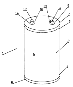
Referring now to Figure 1, there is illustrated one embodiment of an energy
storage device according to the invention in the form of a supercapacitor 1.
Supercapacitor I is packaged in a cylindrical housing 2 which extends axially
between
a first end 3 and a second spaced apart end 4. In other embodiments
differently
1o configured housings are used.
The housing has a cylindrical sidewall 6 and, disposed adjacent to respective
ends 3 and 4, a circular top 7 and base $. All adjacent edges of the base,
sidewall and
top are sealingly engaged. In this embodiment housing 2 is formed from metal
and
top 7 and base 8 are sealingly adhered to sidewall 6.
15 Top 7 includes two diameixically spaced apart ports 9 and 10 for sealingly
receiving respective terminals 11 .and 12. The terminals extend from within
housing 2
where they are electrically connected to respective ones or sets of electrodes
of
supenrapacitor 1. Although a large number of possible electrodes are used in
various
embodiments of the invention, the most preferred will be discussed in more
detail
20~ below.
Terminals 11 and 12 are sealingly retained within the respective ports by
rubber seals 13 and 14.
CA 02348668 2001-04-23
WO 00/34964 PCT/AU99/01081
- 36 -
A first preferred electrode: wnfiguration is illustrated in Figure 2. More
particularly, in this embodiment, supercapacitor 1 includes a plurality of
first sheet
electrodes 21 having respective first tabs 22 extending therefrom. A plurality
of like
second sheet electrodes 23 are alternated with electrodes 21 and have
respective
second tabs 24 extending therefrom. A plurality of porous sheet separators 25
is
disposed between the adjacent electrodes. As described with reference to
Figure 1,
housing 2 contair.~s electrodes 21 and 23, separators 25 and an electrolyte
(not shown).
Tabs 22 are electrically connected to terminal 11 and tabs 24 are electrically
connected
to terminal 12 to allow external electrical connection to the respective
electrodes.
1U It will be appreciated that although in Figure 2 there are illustrated two
electrodes 21 and two electrodes '~3, the actual embodiment includes a far
greater
number of such sheet electrodes which are all interconnected to provide a
predetermined capacitance. The invention, in this form, is particularly
advantageous
in that the modular unit of capacitance - one electrode 21, one electrode 23
and an
15~ intermediate separator 25 - is easily mass produced and combined with a
plurality of
like units to provide the necessary capacitance for a particular application.
Accordingly, a supercapacitor having specific performance characteristics is
able to be
produced easily and in small nurribers at a unit cost not dissimilar to that
of a large
run. In some embodiments a different size housing is required. The relative
cost of
2U~ the housing, however, is not substantive.
Tabs 22 and 24 include respective centrally disposed apertures 27 and 28.
These
apertures receive respective conductive rods 29 and 30 for electrically
interconnecting
CA 02348668 2001-04-23
WO 00/34964 PCT/AU99/01081
-37-
Like tabs. The rods are, in turn, electrically connected within housing 2 to
respective
electrodes 11 and l2.
In some embodiments two adjacent electrodes 21 and 23 are folded together to
reduce one dimension of the electrodes. This is particularly advantageous in
circumstances where the packaging requirements are very specific, although a
known
capacitance is required.
In another embodiment, a similar effect is achieved through use of two or more
sheet electrodes, and one or more intermediate separators, which are wound
together
in a spiral. The two sheet electrodes are longitudinally elongate and
transversely
offset such that their opposed edges define the respective tabs. In this
embodiment,
the length of the sheet electrodes is tailored for the specific capacitance
requirements.
The manufacture of a supercapacitor of this kind will now be described in more
detail.
In other embodiments, such as that described with reference to Figure 1, a
similar
preparation and coating technique is used. However, as will be appreciated by
the
skilled addressee, the sheet electrodes of Figure 1 are stacked rather than
wound.
The supercapacitor is of the double layer type and, for the spiral wound
configuration, one preferred embodiment makes use of aluminium sheet
electrodes
that are 2500 mm long and 85 mm wide. The first step is the preparation of the
coating mixture that contains:
high surface area carbon;
conductive carbon;
binder;
a surfactant; and
CA 02348668 2001-04-23
WO OOI34964 PC'T/AU99/01081
-38-
water.
Although the coating process makes use of a wire-bar technique it will be
appreciated by those skilled in the art that other suitable techniques such as
reverse
roll, doctor blade or the like are also available.
Immediately after the coating procedure is finished, the electrode spools are
placed in an oven to remove any :remaining water and to cure the binder. This
also
prevents corrosion of the alumi.nivm. The oven temperature is maintained in
the range
of 110 °C to 140 "C and preferabay under a fan forced nitrogen
atmosphere. The latter
is to minimise oxidation. The curing time is at least 5 hours, although in
some
1 ~D circumstances it is left longer, such as twelve hours, without any
detriment. Prior to
removing the electrodes, the oven should be allowed to cool to room
temperature to
minimise oxidation.
It is more .convenient to coat the full width of the aluminium foil electrode
and
then slit to the desired width rath~,~r than coat nazrow widths of foil. In
some
1:5 embodiments an uncoated edge is. utilised and the carbon layer is applied
accordingly.
Although the sheet electrode has only been coated on one side, in other
embodiments it includes a coating on both sides. However, in other
embodiments,
raxher than coating both sides, two sheets with a single sided coating are
placed in a
back to back configuration to define a double sided electrode. That is, the
foil
20 electrodes are adhered or otherwise secure together such that the
respective carbon
layer are outwardly facing and opposed to the carbon layers on adjacent
electrodes.
An offset is required between the two electrodes so that each end connection
will only make with one electrode:.
CA 02348668 2001-04-23
WO 00/34964 PCT/AU99/01081
-39-
In embodiments where the terminal is formed by spraying with aluminium, a
flat edge is used to bend the opposed free edges of each electrode over at
90°. This
stops penetration of aluminium spray used in the formation of the terminal.
This
bending is conveniently performed using the flat end of a 20 cm spatula while
the
element is turning. In preferred embodiments approximately 1 to 2 mm of the
edge of
the electrodes are bent over. When looking at the element down the long axis,
no gaps
between electrodes. should be visible.
A more detailed description of the aluminium spraying process is found in co-
pending PCT application number PCT/AU98/00406 the details of which are
1o incorporated herein by way of cross reference.
Briefly, however, it will be noted that the aluminium metal spray is used to
make electrical cormection with the windings. Because of the very high
temperature
of the flame a steady movement of the gun across the elements used, with no
more
than about 1 to 2 seconds on each element at a distance of about 20 cm from
the tip of
the gun. This movement is repeated three times before the elements are turned
and the
remaining side sprayed. This process is repeated as often as required until an
uninterrupted aluminium surface is produced, interspersed with cooling periods
if the
elements are hot to touch. It will be appreciated that the certain separators
have a low
softening temperatizre and will shrink in the cross direction above that
temperature.
2o Once enough aluminium is built up, the ends are ground until a smooth flat
area is obtained sufficient for the terminals to be attached. As a large
amount of heat
is generated during grinding care is. taken not to overheat the capacitor.
This flat area
need not be as large as the whole end but is different for each end. The
bottom end,
CA 02348668 2001-04-23
WO 00134964 PCT1AU99/01081
-40-
that is the end intended to be disposed furthest from top 7, is provided with
an
electrode which is welded with a flat tab that radially extends from the core.
Accordingly, the :flat area that is at least 10 mm wide and which has a smooth
surface
is needed from the core to the edge. The top end terminal is welded
tangentially.
midway between the core and the: edge and so requires about one third or one
half of
the end to be smooth.
Laser welding of the terminal tabs is then undertaken. The equipment was a
Lasag Nd:YAG laser rated at 500 W continuous. At least two 8 mm rows of welds
~3
mm apart were produced on each tab. The beam is moved at about 140 mm/min, and
1o pulsed at 10 Hz with an energy of 29.5 Joules /pulse.
Prior to the final placing o~f the now formed capacitor element into the
package, which is in the form of a~ metal can, Teflon insulators are placed
between the
terminals and the top sprayed aluminium face to stop the terminal from the
bottom
touching the top face and producing a short circuit. This insulator is a 1 mm
thick
i5 Teflon disk with a. 3 mm hole punched in the center with a radial slit firm
this hole to
the edge. This hole locates the insulator on the center terminal and prevents
this
terminal from touching the aluminium end connection. A circular disk of Teflon
is
also placed in the package to insulate the bottom of the element from the can.
In most
cases, polypropylene foam is disposed in the base of the can to hold the
element in
2o place. In other embodiments, however, use is made of a formed plastic
locater.
Once the capacitive element is in the can, a final drying step is carried out
to
remove any moisture. This is carried out in a vacuum oven at a maximum
temperature
of 80°C. This low temperature avoids softening of the separator. The
low
CA 02348668 2001-04-23
WO 00/34964 PCT/AU99/01081
-41 -
temperature drying is carried out for about 12 hours using a rotary vacuum
pump,
capable of producing a vacuum of better than 150 Pa.
Electrolyte is then added to the can so that the capacitive element, excluding
the upwardly extc;nding terminals,, are completely covered. The pressure in
the oven is
gradually reduced to about 53 Pa such that air trapped in the carbon pores is
removed.
When the initial degassing has subsided, the vacuum is increased to 8 Pa. This
process
is facilitated by warming the oven to 60 °C. After about 30 minutes
degassing should
have substantially stopped and the oven is brought to atmospheric pressure
with
nitrogen. Thereafter the capacitors are removed from the oven. More
electrolyte is
1c) added and the process repeated until no more electrolyte is taken up. It
is usual for 2
or 3 cycles to be c;ompleted. Finally, any excess electrolyte is removed.
The capacitor is then completed by mounting the top on the terminals. In this
embodiment the top is made of Bakelite, although in other embodiments other
materials are used. The top edge of the can is curled over the periphery of
the top
1~~ using a sealing tool in a small drill press at 100 rpm.
Preferably, two types of c~~rbon are used in the capacitor. First, a high
surface
area or active carbon ands secondly, a carbon such as a conductive carbon
black.
The electrodes are preferably aluminium foil.
The electr,~lyte, in this eiribodiment, consists of a 1.0 M solution of
2G tetraethylammonium tetrafluoroborate (TEATFB) dissolved in propylene
carbonate
(PC). That is, 21 i' grams of TEA'fFB in 1 litre of solution. The amount of
water in
the electrolyte is kept to an absolute minimum and preferably less than SO
ppm.
Accordingly, anhydrous PC is used, such as that produced by Sigma Aldrich.
CA 02348668 2001-04-23
WO OOI34964 PC'T/AU99/01081
- 42 -
Moreover, the TEATFB is exhaustively dried prior to use. This drying is
achieved by
vacuum oven drying at 160°C for about six hours or such time that is
sufficient to
adequately reduce the moisture content.
The TEA.TFB is slow to dissolve, and at room temperature it is not unusual to
allow 24 hours for it to fully dissolve. The present preferred method,
however,
reduces this time; by warming the solution to SO°C. To keep the
moisture content low,
the preparation o~f electrolyte is performed inside a dry nitrogen glove box.
The separator has desirable porosity, strength and thinness for use in the
present invention.
to An alternative embodiment of the invention is illustrated in Figure 3
and.Figure
4. In this embodiment, the basic capacitive unit includes of two like sheet
electrodes
35 and 36 which., as best shown i.n Figure 4, are folded together. Each sheet
electrode
is rectangular an<i includes four adjacent edges 37, 38, 39 and 40. Extending
outwardly from edge 40 are two ~symmetricaliy spaced apart tabs 41 and 42
having
15 respective apertures 43 and 44. These tabs function similarly to tabs 22
and 24 of
Figure 2 in that they are connected together with a plurality of like tabs and
collectively electrical joined to a terminal 11 or 12 of capacitor 1.
In use, each of electrodes 35 and 36 are centrally folded about an axis 45
which
is parallel to edges 37 and 39. As shown in Figure 4, each electrode is
interleaved
2.o with the other such that edge 39 of each electrode lies adjacent to axis
45 of the other
electrode. Also included between each adjacent portion of the electrodes is a
porous
separator 46. It will be appreciated that the Figure 4 illustration is
schematically
represented to assist an understanding of the configuration of this
embodiment. In
CA 02348668 2001-04-23
WO 001349b4 PCT/AU99/01081
- 43 -
practice the adjacent electrodes and separators are immediately adjacent each
other
rather than the spaced apart configuration shown in Figure 4.
Electrodes 35 and 36 include on each side a layer of activated carbon that is
applied as described above. However, as would now be appreciated by those
skilled
in the art the winding step of the above method would be substituted with a
folding
and then a stacking of a predetennined plurality of capacitive elements to
provide
supercapacitor 1 with the desired electrical characteristics.
Where use is made of a plurality of capacitive elements, a porous separator is
disposed between adjacent elements to prevent electrical shorting.
In some embodiments eleclxodes 35 and 36 are initially coextensively abutted
with a separator and then folded together.
In other embodiments edge 40 of one electrode lies adjacent to edge 38 of the
other electrode such that tabs 41 and 42 extend away from each other. In some
such
embodiments each electrode is folded together with the other, and the
intermediate
~ 5 separator, along a plurality of axes, each of which is parallel and spaced
apart from
axis 45. In still fiirther embodiments the electrodes are folded along one or
more axes
which is or are narmal to axis 45. In alternative embodiments electrodes 35
and 36
are folded along at least one axis parallel to axis 45 and at least one axis
normal to axis
45.
2,0 To further illustrate the invention and its applications it is useful to
look at the
theoretical and practical underpinnings of supercapacitor development. More
particularly, it will be appreciated that the supercapacitors of the invention
are capable
of being used in high power applications. The characteristics of such
supercapacitor
CA 02348668 2001-04-23
WO 00/34964 PCT/AU99/01081
dictate the efficiency, size and mass required for the application. For a
given mass or
volume and capacitance it is the characteristic of electrical resistance
(known as the
equivalent series resistance or esr) which distinguishes high from low
efficiency
supercapacitors. 'That is, for high power applications a low esr is desired to
minimise
~~ losses.
For any capacitor the electrical resistance can be lowered by increasing mass
and volume. However, the desired result is a simultaneous decrease in
resistance,
mass and volume while maintaining capacitance.
The factors that contribute; to electrical resistance include: the intrinsic
electrical conductivity of the carbon, for carbon based supercapacitors; the
interfacial
resistance; the metallic electrode and connection resistance; and the
electrolyte and
separator resistance. Attempts have been made to minimise these factors to
achieve
high efficiency operation.
In a traditional capacitor, t:he current flow is between two flat electrodes
separated by a dielectric. Although carbon based capacitors appear to be
constructed
in a similar fashion, the material between the metallic electrodes is not the
dielectric,
but the high surface area carbon, electrolyte and separator (the active
materials). The
dielectric is the nanometer thin layer of solvent at the carbon surface. As
the current
flows from the metallic electrodes, through these materials, their resistance
must be
minimised to reduce the esr of the capacitor. This is achieved by reducing the
thickness of the active materials, for example by increasing the density of
the carbon
coating or using thinner coatings. Another approach along these lines is to
use thinner
CA 02348668 2001-04-23
WO 00/34964 PC'T/AU99/01081
-45-
separators. The re;ducdon of thicltness also reduces the resistive component
of the
electrolyte by minimising the path through which the current must flow.
Another means of reducing the resistance of the active materials is to use
more
conductive carbons and electrolytes. The combination of more conductive active
materials with thinner design allows higher powers to be achieved while
maintaining
or reducing the mass and/or volume.
The product of resistance and capacitance (RC), commonly referred to as the
time constant, is frequently used to characterise capacitors. In an ideal
capacitor, the
time constant is frequency independent. However, in carbon based
supercapacitors,
both R and C are frequency dependent. This arises from the microporous
characteristics of high surface area carbons, and the nature of charge build
up at the
electric double layer on the carbon surface. The traditional method of
measuring R
and C for supercapacitors is to use a constant current charge or discharge and
to
measure the voltage jump at the start or finish of the cycle, and the rate of
change of
voltage during the cycle respectively. This however effectively provides the R
at high
frequency and the C at Iow frequency. Another more suitable method is to
measure
the frequency response of the complex impedance and to model a simple RC
element
to the data. This provides an estimate of R and C across the frequency range
that may
or may not correlate with those measured using constant current techniques.
Clearly,
2C~ the use of RC time constant as a measure of capacitor suitability is
subject to a large
uncertainty. A more useful technique has recently been proposed in which R and
C
are measured at the frequency at which the phase angle of current and voltage
is -45°.
The reciprocal of this frequency is the "response time" and is more clearly
defined
CA 02348668 2001-04-23
WO 00/34964 PCT/AU99/Ot081
than other methods. Further, thc; capacitance at this frequency can then be
used to
calculate the energy and provide a Figure of Merit (FOM) when normalised with
mass
or volume.
The theoretical maximum power available from any capacitor is the quotient of
the voltage squared over four times the esr. When normalised to mass or volume
this
provides the theoretical maximum power density in W/kg. Clearly the maximum
power can be in~,~reased by either decreasing the resistance (as shown above),
increasing the operating voltage, or both. Increases in operating voltage can
be
achieved, without any change in the composition of the supercapacitor
materials, by
1o maximising the voltage window in which the capacitor operates. In a
supercapacitor
with symmetrical carbon based electrodes, the voltage is equally distributed
across
both electrodes. During operation, the maximum capacitor voltage is limited by
the
breakdown voltage of the weakest electrode. A higher operating voltage can be
achieved by tailoring the capacitance of each electrode to fully utilise the
available
voltage window. This is conveniently achieved by using different carbon
loadings on
each electrode.
Aspects of the invention described in this specification allow targeted energy
and power densities to be achieved by a novel supercapacitor design and the
associated manufacturing process. One result is an extremely thin, high power
zo capacitor suitable for mobile telecommunication applications. Another is
suitable for
Load-leveling in hybrid electric vehicles. Specific examples of these will be
fiuther
illustrated by the following description.
EXAMPLES
CA 02348668 2001-04-23
WO 00/34964 PCT/AU99/01081
-47-
Example 1
As schematically shown i.n Figures 5 to 7, a supercapacitor 51 includes a
first
electrode in the f~nn of a first ph.~rality of spaced apart rectangular
aluminium sheets
52. A second electrode in the foam of a second plurality of spaced apart
rectangular
aluminium sheets 53 are interleaved with and opposed to sheets 52. A plurality
of
porous separators 54 are interposed between the adjacent sheets 52 and 53. A
rectangular sealed plastic package 55 contains electrodes 52 and 53,
separators 54 and
an electrolyte 56 in which the electrodes are immersed. In this embodiment the
electrolyte is acet:onitrile with TE,ATFB. A rectangular tab 57 and a
rectangular tab 58
l0 are integrally formed with and upwardly extend from respective ones of
sheets 52 and
53. Tabs 57 are abutted together and electrically connected to a terminal 59,
while
tabs 58 are abutted together and electrically connected to a terminal 60. This
electrical
connection is affected in this embodiment with ultrasonic welding. Both
terminals 59
and 60 extend from package 55 to allow external electrical connection to the
1 ~ respective electrodes.
Each of sheets 52 and 53 have a width of about 70 xnm, a height of about 170
mm and a thickness of about 20 microns. In this particular embodiment use is
made
of fifty of each of sheets 52 and 53, in that there are 100 sheets in total.
This provides
a total electrode area of 5950 cm2.
20~ As shown in the drawings, sheets 52 and 53 are each coated on a single
side only
with an activated carbon layer 62, as described with reference to the earlier
embodiments. Where appropriates two like sheets are abutted back to back to
provide
outwardly facing activated carbon layers that are opposed by like carbon
layers on the
CA 02348668 2001-04-23
WO 00/34964 PCT/AU99/01081
-48-
other of the sheets. In this embodiment layer 62 is substantially uniform
across the
sheets and has a thickness of about 36 microns.
Package SS has a rectangular prismatic form made from ABS having external
dimensions of about 17 mm by 110 mm by 190 mm. Where terminals 59 and 60
extend through the package appropriate sealant 61 is used to prevent egress of
electrolyte 56 from package SS or, also importantly, the ingress of air,
moisture or
other contaminants into package :SS.
As will be appreciated by those skilled in the art separator 54 maintains the
opposed layers 62 in a spaced apart configuration to prevent electrical
conduction
1~D therebetween. However, separators 52 do allow movement of the ions within
the
electrolyte between layers 62. In this particular embodiment separators 54 are
folded
around back to back pairs of sheets 53.
Supercapacitor 51 is rated at 2.5 Volts and provides a nominal capacitance of
270 Farads. Impartantly, however, the overall weight, including the
electrolyte and
1:> packaging, is 295 grams. Utilising these figures, in combination with a
measured To
of 1 second provides a gravimetric FOM of 2.2 Watts/gram and a volumetric FOM
of
1.6 Watts/cm3.
When utilising the; simple RC model the equivalent series resistance is about
1 mS2
and the RC time constant is about 280 ms.
2c~ Ezample 2
Another specific example of a supercapacitor 71 made in accordance the
invention is schematically illustrated in Figures 8 and 9. In these Figures
corresponding features are denoted by corresponding reference numerals.
CA 02348668 2001-04-23
WO 00/34964 PCT/AU99/01081
-49-
Each of sheets 52 and 53 have a width of about 40 mm, a height of about 40 mm
and a thickness of about 20 microns. In this particular embodiment use is made
of
forty of each of sheets 52 and 53, in that there are eighty sheets in total.
This provides
a total electrode area of 640 cmz.
In this embodiment layer 6:? is again substantially uniform across the sheets
and
has a thickness of about 36 microns.
Package 55 has a rectangular prismatic form made from ABS having external
dimensions of about 10 mm by 50 mm by 50 mm.
Supercapaci.tor 71 is rated at 2.5 Volts and provides a nominal capacitance of
30
1~~ Farads. The over;~.ll weight, including the electrolyte and packaging, is
25 grams.
Utilising these figures, in combination with a measured To of 0.48 second
provides a
gravimetric FOM of 2.71 Watts/gram and a volumetric FOM of 2.71 Watts/cm3.
When utilising thc; simple RC model the equivalent series resistance is about
4 mS2
and the RC time constant is about 120 ms.
1:5 Example 3
Another specific example of a supercapacitor made in accordance the invention
is of the same construction of that shown in Figures 8 and 9. However, in this
embodiment use is made of twenty of each of sheets 52 and 53, in that there
are forty
sheets in total. This provides a total electrode area of 320 cm2.
20 In this embodiment layer 62 is again substantially uniform across the
sheets and
has a thickness of about 12 micros.
Package 55 has a rectangular prismatic form made from ABS having external
dimensions of about 5 mm by 50 ~nm by 50 mm.
CA 02348668 2001-04-23
WO 00/34964 PCT/AU99/01081
-50-
The superc;ipacitor of this example is rated at 2.5 Volts and provides a
nominal
capacitance of 10 Farads. The overall weight, including the electrolyte and
packaging,
is 17 grams. Utilising these figures, in combination with a measured To of
0.11
seconds provides a gravimetric FOM of 2.64 Watts/gram and a volumetric FOM of
:> 3.00 Watts/cm3.
When utilising the simple RC model the equivalent series resistance is about 5
mS2
and the RC time constant is about 50 ms.
Example 4
There is shown in Figures 10, 11 and 11A a supercapacitor 81, where
1U corresponding features are denoted by corresponding reference numerals. As
with the
other examples described above, use is made of sheet electrodes. However,
these
sheets are contained within a package 82 the size of a credit card or smart
card.
Each of sheets 52 and 53 have a width of about 40 mm, a height of about 65 mm
and a thickness of about 20 microns. In this particular embodiment use is made
of
1 ~, three of each of sheets 52 and 53, in that there are six sheets in total.
This provides a
total electrode area of 78 cm2.
Again, layer 62 is substantially uniform across the sheets and has a thickness
of
about 12 microns.
Package SS has a rectangul~~r prismatic form made from PVC sheets and having
20~ external dimensions of about 2 mm by 54 mm by 86 mm.
Supercapacitor 81 is rated at 2.5 Volts and provides a nominal capacitance of
0.3
Farads. .The overall weight, including the electrolyte and packaging, is 12
grams.
CA 02348668 2001-04-23
WO 00/34964 PCT/AU99/01081
-S1-
Utilising these figures, in combination with a measured To of 0.037 seconds
provides a
gravimetxic FOM of 1.27 Watts/gram and a volumetric FOM of 1.68 Watts/cm3.
When utilising the simple RC model the equivalent series resistance is about
22.5 mS2
and the RC time constant is about 6.3 ms.
Examele 5
A multiple charge storage; device' in the form of a supercapacitor 90 is
schematically illustrated in Figure 18. Supercapacitor 90 includes a first
sheet
electrode which is collectively defined by aluminium sheets 94 and 96. In
other
embodiments a single folded sheet is used. It will be appreciated by those
skilled in
1t~ the art that a single sheet could also be used.
Both sheets 94 and 96 are electrically connected to a first terminal (not
shown).
Sheet 94 includes a first coating ~>5 on one side thereof, while the opposite
side of
sheet 96 includes a second coating 97. The first coating is of a first
predetermined
thickness and the second coating is of a second predetermined thickness which
is
1:. different from the first thickness. A second sheet electrode 98 is
electrically
connected to a second terminal 92 and is disposed adjacent to the one side of
electrode
94. Also, electrode 98 includes a third coating 199 on one side thereof of a
third
predetermined thickness which is equal to the first predetermined thickness.
Coating
199 is opposed to coating 95. A third electrode 200 is electrically connected
to
2U terminal 92 and is disposed adjacent to sheet 96. Electrode 200 includes a
fourth
coating 201 on one side thereof which is of a fourth predetermined thickness.
Moreover, coating 201 is opposed to coating 97. As with other embodiments, a
plurality of porous separators are disposed between respective adjacent
electrodes.
CA 02348668 2001-04-23
WO 00/34964 PCT/AU99/01081
-52-
Additionally, supercapacitor 90 includes a package 91 for containing the
electrodes,
the one or more separators and an electrolyte and through which the terminals
extend
to allow external electrical connection to the respective electrodes.
All the coatings of this embodiment utilise the same formulation. The
differing
thicknesses, however, provide supercapacitor 90 with a multiple time constant
given
that the two capacitive cells making up the supercapacitor are in parallel
with each
other. In this case, a cells are defined by the respective opposed and
adjacent carbon
coatings.
In other embodiments the thicknesses of the coatings are the same and the
to formulation of the coating varies between cells to provide a difference in
capacitance.
This, in turn, provides a multiple time constant supercapacitor.
Example 6
An alternative multiple charge storage device in the form of supercapacitor 99
is schematically illustrated in Figure 19. This supercapacitor includes a
first sheet
is electrode 100 which is electrically connected to a first terminal (not
shown) aad which
includes a first coating 102 on one side thereof having a first predetermined
thickness.
A second sheet electrode 103 is electrically connected to a second terminal
(not
shown) and is disposed adjacent to electrode 100. The second electrode
includes a
second coating 106 on one side thereof having a second predetermined
thickness. As
2o shown, coating l0fi is opposed to coating 102.
A porous separator 54 is disposed between the adjacent electrodes for
maintaining those electrodes in a fixed spaced apart configuration.
Additionally, a
package 105 contains the electrodes, the separator and an electrolyte, whereby
the
CA 02348668 2001-04-23
WO 00/34964 PCT/AU99/01081
-53-
terminals (not shown) extend from the package to allow external electrical
connection
to the respective electrodes.
This arrangement of a varying carbon thickness across the separate electrodes
also provides a multiple time corustant supercapacitor.
For convenience, the electrode pair shown in Figure 19 is defined as a cell.
In
other embodiments, use is made of a plurality of like cells stacked together
and
connected in paralel to provide the desired capacitance. Preferably, also, the
cells are
stacked such that the thinner end and the thicker end of one cell are
juxtaposed to the
respective thicker end and the thinner end of at least one adjacent cell.
1.o In other embodiments use is made of constructions similar to that of the
above
examples but with different physical parameters to provide different
characteristics.
Some examples of such alternative physical parameters and resultant
characteristics
are shown in the Table of Figure 17 and Figure 20. For ease of reference,
Figure 12
provides a graphical representation of the gravimetric FOM versus To for the
examples
~ 5 of the invention listed in Figure 17, where the respective locations of
the
supercapacitors on the reference plane are represented by numerals
corresponding to
the item number in the Table of Figure 17. Figure 13 provides a corresponding
representation for. the example supercapacitors showing volumetric FOM versus
To.
The supercapacitor shown as Item 12 in Figure 17 includes a parallel
2:o combination of pairs of capacitive cells that are connected in series.
Accordingly, the
nominal operational voltage is 5 'Volts. In other embodiments more than two
capacitive cells are connected in series to provide a higher operating
voltage.
CA 02348668 2001-04-23
wo oor~a~a Pc riAUmo~og~
-54-
It is also useful to characterise the capacitors of the present invention with
criteria more commonly used in the field. More particularly, the maximum power
(PBX) available from a supercapacitor has been calculated with the formula:
P~"~ = VZ/4R
where V is the maximum operating voltage of the capacitor and R is the
resistance
determined from the simple RC model of the capacitor.
The Pr"aX values for the examples in Figure 17 have been calculated and
divided,
on the one hand by the mass of the respective devices to provide a gravimetric
P",aX
and, on the other hand, by the volume of the respective devices to provide a
1o volumetric P1"aX. These values have then been plotted in Figures 14 and 15
respectively against time constanus.
As particularly illustrated ix~ Figures I2 to 15 inclusive, the
supercapacitors
described in the e:rcamples above provide extremely advantageous pulse power
load
characteristics. That is, a low response time Ta and time constant ensures
good
15 transient response to high frequency loads, as are encountered in
applications where
switching or pulsing of the load occurs. This, in combination with the high
gravimetric FOM and Pte, and tt~e high volumetric FOM and PT"~ provided in the
examples, allow the invention to be applied to a broad range of applications.
To
illustrate this point, the supercapacitor of Example 1 is intended primarily
for high
2o power automotive applications to facilitate regenerative breaking and the
provision of
high torque over short time periods, and the necessity for correspondingly
high current
loads. The supercapacitor of Exa'nple 4, however, is primarily intended to be
used in
parallel with a mobile telephone battery.
CA 02348668 2001-04-23
WO 00/34964 PCT/AU99/01081
-SS-
The graphs of Figures 12 t~o 1 S each include two unbroken lines, which extend
across the upper regions of the r<mges shown. In each case the lines represent
the
theoretical upper Iimit of the various parameters being illustrated for the
examples 3
and 12 shown in Figure 17. For a given combination of features and the given
formulation of the carbon coating, there will be a theoretical maximum where
the
volume or mass contribution of the packaging to the overall device is small.
For other
formulations the theoretical maximum will differ.
With the benefit of the teaching herein the skilled addressee would appreciate
that the invention. is also advantageous in that various parameters of the
supercapacitor
In are easily tailored to meet the specific requirements of any particular
application. That
is, the invention is particularly suited to scaling. By way of example, Figure
16 shows
various calculated characteristics for a number of other embodiments of the
invention.
This illustrates that for a given formulation, thinner layers higher provide
higher
power densities and figures of merit, as well as lower time constants and
response
1:i times.
It will be understood that the unbroken lines included in the Figures
represent
the limit for the tvvo given formulations. However, there are other
formulations which
provide an extended range of operability and allow higher figures of merit and
power
densities, as well as lower time constants, to be achieved.
2n The calculations in Figure lt6 are based on the resistance ofthe devices
being
comprised of the resistance of
1. the terminals;
2. the aluminium electrodes;
CA 02348668 2001-04-23
WO 00134964 PCT/AU99/01081
-56-
3. the electrode/carbon interface;
4. the carbon inter-particle interface;
5. the electrolyte in the carbon layer; and
6. the electrolyte in the sparator.
The present invention makes use of this model to optimise the various
resistances while: still providing .a high capacitance, high figures of merit,
high power
densities and a desired response time.
The gravimetric FOM is expected to scale as the gravimetric power density,
and the volumetric FOM is expected to scale as the volumetric power density.
These
to latter quantities are proportional to: V2; 1/R and either 1/mass or
l/Volume. Thus, for
a given voltage optimised for the application, an increase in FOM comes
through
decreasing R, decreasing mass and decreasing volume. For a given formulation
and
given thiclrness of coating R is essentially proportional to the inverse of
the electrode
area. For minimal packaging mass or volume, the mass and volume are
proportional
i5 to the electrode area. Thus making a "bigger" device will only marginally
increase the
FOM due to less packaging. Hence, for a given size of device, the resistance
is
minimised by decreasing the thiclrness of the coating consistent with the time
constant
or response time desired for the device. The capacitance of the device is then
determined by the selection of the; mix of carbons and the formulation of the
coating
2~D material.
The inventors also believe that the superior performance of supercapacitors of
the present invention is contributed to by the improved conductivity between
individual carbon particles resulting from the use of the mixture of carbon
particles
CA 02348668 2001-04-23
WO 00/34964 PCT/AU99101081
-57-
and protonated carboxy methyl cellulose (CMC). Without wishing to be bound by
theory, it is believed that such improved conductivity is the result of a
number of
factors such as increased packing density of individual carbon particles;
increased
migration of electrolyte into infra-molecular spaces on the surface of the
individual
carbon particles; and an overall reduction in the size of the interface region
between
the carbon particles and electrolyte. It is believed that a mixture of high
surface area
carbon and highly conductive carbon optimises these effects.
Further, the, relative insolubility of protonated CMC contributes to an
increased
overall life of the supercapacitors of the present invention.
to It will be appreciated that the term "immersed" or like terms, unless
explicitly
noted otherwise, when used in reference to the disposition of the electrodes
in the
electrolyte is intended to include not only those supercapacitors where an
excess of
electrolyte is used, but also those where the quantity of electrolyte is
sufficient to only
wet the electrode:.. That is, the quantity of electrolyte need be sufficient
to allow
1 s operation of the supercapacitor.
It will also be appreciated that although the above examples are primarily
concerned with discrete cells, the invention is also applicable to bipolar
configurations.
Moreover, it will be appreciated that the term "organic electrolyte" or like
terms
2n~ refer to an electrolyte in an organic solvent.
For comparative purposes Figure 17 provides a Table showing parameters of
supercapacitors of the present invention as well as some prior art
supercapacitors.
CA 02348668 2001-04-23
WO 00/34964 PCT/AU99/01081
-58-
Referring to Figure 21, a charge storage device 301 includes a sealed
prismatic
housing 302. Two opposed folded rectangular aluminium electrodes 303 and 304
are
disposed within housing 302 and connected to respective metal terminals 305
and 306
for allowing external electrical connection to the electrodes. A SoluporTM
sheet
separator 307 is disposed intermediate electrodes 303 and 304 for maintaining
those
electrodes in a fixed spaced apart: configuration. An electrolyte (not shown)
is also
disposed intermediate the electrodes.
Separator 307 is formed in a "pocket" configuration, wherein it is folded back
upon itself and the transverse ends secured together for providing an opening
308
n) between the transverse ends. For ease of illustration, separator 307 is
shown as having
two fold lines. In practice, however, a single fold line is used as the
separator is
abutted directly against the opposed electrodes. The porous nature of the
separator
allows the movement of ions in the electrolyte between the electrodes.
Each electrode is formed from a single like aluminium sheet having at least
one
15 tab 309 which is c;lectrically engaged with the respective terminals 305
and 306. The
electrodes are folded into the overlapping and nested configuration shown in
the
drawing. Again, iit will be appreciated that for ease of illustration
electrode 304 is
shown with two field lines. In practice, however, a single fold is made as
this
electrode is abutted directly against separator 307.
2o Electrode 31)3 is received vcrithin opening 308 and enveloped by separator
307
such that only tab 309 extends from the "pocket" or pouch. This electrode and
separator combination is then inserted into the folded electrode 304 to
complete a
single capacitive cell. While in this embodiment only a single cell is
illustrated, in
CA 02348668 2001-04-23
WO 00/34964 PCT/AU99/01081
-59-
other embodiments use is made of two or more such cells. The electrode area of
the
electrodes is about 102 cm2 which provides a nominal capacitance of about 28
Farads
at 2.5 Volts.
Each of electrodes 303 and :304 includes a high surface area coating 310 of
activated carbon. This coating is of a predetermined thickness and includes a
binder
to facilitate intimate engagement between the carbon and the electrodes.
As terminals 305 and 306 extend from the inside to the outside of housing 302
they are sealingly engaged intermediate their respective ends with the
housing. In this
embodiment the sealing engagement is effected by two rubber grommets 311 and
312.
In other embodiments use is made of grommets constructed from other materials
or
combinations of materials. For example, some devices make use of silicon
sealing
compounds and adhesives.
Electrode 3CI3 and 304 will now be described in more detail with reference to
Figures 22 to 24. More particularly, and as best shown in Figure 23, electrode
303 is
~5 substantially rectangular and includes two rectangular sub-sheets 315 and
316. The
sub-sheets are integrally formed and symmetrical about a fold line 3 i 7 which
defines
a common edge 318. Sheets 315 and 316 include respective integrally formed
rectangular sub-tabs 319 and 320 which, as shown in Figure 24, abut to
collectively
define tab 309.
2o Sheet 315 includes two spaced apart and parallel edges 321 and 322 which
extend away normally from edge 3I 8. A further edge 323 extends between edges
321
and 322. As also shown in Figure 23, tab 319 extends from away from edge 323
adjacent to where that edge meets with edge 322. Similarly, sheet 316 includes
two
CA 02348668 2001-04-23
WO 00/34964 PC'T/AU99/01081
-60-
spaced apart and parallel edges 325 and 326 which extend away normally from
edge
318. A further edge 327 extends between edges 325 and 326. Similarly also, tab
320
extends from away from edge 32.7 adjacent to where that edge meets with edge
326.
Electrode 303 is coated on one side only with the activated carbon and then
folded about line; 317 such that the coated side is outwardly facing, as shown
in Figure
21.
Electrode 304 is the same ~~s electrode 303 only that it is interleaved in the
opposite sense so that the respective tabs 309 are spaced apart. This will be
described
in further detail below. For convenience, corresponding features of the
electrodes will
1~~ be designated with corresponding reference numerals.
Separator 307 is shown, not to scale, in plan in Figure 22 and includes two
rectangular sub-sheets 331 and 332 which are integrally formed along a common
edge
333. This edge also defines a fold line 334. Sheet 331 also includes two
spaced apart
and parallel edges 335 and 336 which extend away normally from edge 333. A
free
1.5 edge 337 extend:. between edges 335 and 336. Similarly, sheet 332 includes
two
spaced apart and parallel edges 339 and 340 which extend away normally fibm
edge
333. A free edge 341 extends between edges 339 and 340.
During manufacture, electrode 303 is folded about line 317 such that the
coated
sides of sheets 31'.5 and 316 are opposed and outwardly facing. Additionally,
tabs 319
20 and 320 are abutted. Separately, separator 307 is folded about line 334
such that
edges 335 and 339 are parallel and abutted together, edges 336 and 340 are
parallel
abutted together and edges 337 and 341 are parallel and adjacent to one
another.
Thereafter, edges 335 and 339 are joined together and edges 336 and 340 are
joined
CA 02348668 2001-04-23
WO 00/34964 PCT/AU99/01081
-61-
together. In some embodiments this is achieved with adhesive, while in other
embodiments heat welding or other heat treatment is utilised. In still further
embodiments the edges are not joined.
As best illustrated in Figure: 24, electrode 303 is then nested within the
"pouch"
or "pocket" formed by separator :307. As shown, the separator envelopes
substantially
all of electrode 303 and, as will be described below, maintains electrodes 303
and 304
in a spaced apart configuration. Tab 309 extends outwardly beyond adjacent
edges
337 and 341 to allow its electrical connection to terminal 305. For ease of
illustration,
in Figure 24 the separator 307 is shown with edges 336 and 340 joined by way
of heat
1n welding, while edges 335 and 339 are adjacent, although not yet joined.
Electrode 304 is then formed by folding a like coated sheet to that which
forms
electrode 303. More particularly, the fold is made along fold line 318 such
that that
the coated sides of sheets 315 anf. 316 are opposed and inwardly facing.
Additionally,
tabs 319 and 320 are adjacent to each other and opposed. The assembly of
Figure 24
15 is then nested within electrode 304, as best illustrated in Figure 25, such
that the
respective tabs 309 of the electrodes are spaced apart. Tabs 319 and 320 of
electrode
304 are then abutted and secured to terminal 306 to allow external electrical
connection with the electrode.
The electrode assembly of F figure 25 is referred to as s single cell and, as
would
2~) be appreciated by a skilled addressee from the teaching herein, a
plurality of the cells
are able to be connected in parallel to proportionally increase the
capacitance of
supercapacitor 301. In other embodiments, a plurality of the cells are stacked
in
parallel such that the respective tabs 309 for like electrodes 303 and 304
form two
CA 02348668 2001-04-23
WO 00/34964 PCT/AU99/O10$1
-62-
spaced apart stacks of like tabs. 'fhe tabs in each stack are then clamped
together and
the stacks electrically connected to respective terminals 305 and 306.
The prefen:ed embodiments of the invention use a non-aqueous electrolyte to
achieve high enerlry densities. Surprisingly, however, they are also able to
achieve
high power densities and FOM's in spite of the conventional wisdom to the
contrary
for this type of electrolyte. This result is achieved in the preferred
embodiments
through a concerted effort to reduce the overall resistance of the
supercapacitor. The
use of the following features contribute to this result:
~ a thin highly porous separator to minimise the length of the current path,
and hence
the resistance, offered by the electrolyte;
~ thin layers of high surface area carbon (less than about 100 microns thick)
for
providing a short current path through the carbon to the aluminium electrode
while
still providing a high capacitance per unit volume;
~ a blend of carbons including conductive carbon black for improving the
conductivity of the carbon layer; and
~ an electrolyte including a high concentration of salt (in the order of 1.0
Molar).
In some embodiments the thickness of each carbon coating, including the
binder,
is less than 100 microns. For the examples shown in Figures 17 and 20 the
respective
carbon coating thicknesses are specified. With the exception of the 6 micron
coating,
2o the carbon particle diameter is a nominal 6 to 8 microns. However, for the
6 micron
coaxing use is made of similar size particles that are ground to a nominal
diameter of 2
microns. In embodiments where use is made of smaller nominal diameter carbons,
the
coatings are thinner again.
CA 02348668 2001-04-23
WO 00/34964 PCT/AU99/01081
- 63 -
The conventional wisdom has been to utilise relatively thick carbon coatings
to
provide a greater capacitance per unit volume. Such coatings are in the order
of about
150 microns or greater. However, it has been discovered that thinner coatings,
as used
in the described embodiments, allows a reduced esr as the length of the
current path
:i through the carbon coating is small. The thin coatings also have a positive
contribution to a high FOM's as they occupy less volume than the thicker
coatings
employed in prior art devices. Surprisingly, however, the devices according to
the
preferred embodiments of the invention still provide relatively high
capacitance as the
available surface area remains relatively high due to the use of an activated
carbon and
to a protonated binder.
While not wishing to be limited by theory, it is presently understood, when
thinner coatings are used, that another mechanism comes into play. More
particularly,
the activated carbon used in the preferred embodiments results in
interparticle voids in
the carbon coating. These voids are typically labrinthine in character. For
prior art
1 ~> coatings having a thickness which is significantly greater than the
carbon particle size,
the impedance of 'the coating is high. However, for the coatings of the
preferred
embodiments, where the coating thickness is the same order of magnitude as the
carbon particle size, the effect of the interparticle voids is minimal on the
impedance.
That is, it has been discovered that there is a strong relationship between
the size of
2o the active carbon particle, the thickness of the carbon layer and the
resultant
impedance provided by that layer.
CA 02348668 2001-04-23
WO 00!34964 PCT/AU99/01081
Preferred embodiments of the invention make use of thinner carbon coatings to
take advantage of this relationship and thereby achieve greater capacitances
per unit
volume, and hence high FOM's.
The volume and mass measurements for determining FOM's take into account
the packaging in which the electrodes, the separator and electrolyte are
contained. The
high FOM's achievable with the described embodiments of the invention are also
contributed to by the packaging itself and the compact method of disposing the
separate components within the packaging.
For the larger supercapacitors constructed in accordance with the invention it
is
to known to use hea~~ier and bulkier packaging than is absolutely necessary
and still
achieve relatively high FOM's. For example, in cases where it is desirable to
have
highly robust packaging for operation in hostile environments some compromise
in
FOM is tolerated. However, for these larger devices, the relatively high FOM's
are
still possible due to the packaging contributing proportionally less to the
overall
1s volume or weight of the device.
For some of the smaller devices, the high FOM's are achieved, in part, through
use of flexible mufti-layer plastics packaging. Examples of such packing are
disclosed
in the co-pending :international Patent Application no. PCT/AU99/00780 in the
name
of the present applicants. The disclosure within that PCT application is
incorporated
2o herein by way of cross reference.
Although the invention has been described with reference to specific examples
it
will be appreciated by those skilled in the art that it may be embodied in
many other
forms.