Note: Descriptions are shown in the official language in which they were submitted.
CA 02348983 2001-04-26
WO 00/26917 PCT/IB99/01732
MICROELECTRONIC CHIPS
The present invention relates to microelectronic chips for enabling high speed
1/O
data port communication with network DRAM banks, and the like, being more
particularly, though not exclusively, directed to chip layouts particularly
tailored for
operation with the universal multi-port internally cached DRAM bank high speed
switching techniques described in llSukesh Chatter LT.S. Patent 5,799,209 and
published
in PCT publication document WO97/24725.
BACKGROUND
Many approaches have been used for the Layout of various types of network
switching and communication chips. Prior chip layout schemes have not,
however, been
suited to accommodating the operation and extremely high switching speeds and
other
quite different characteristics of the above-mentioned Chatter, universal
multi-port
internally cached DRAM bank operation. In such, wherein there is provided a
switching
module logic control for connecting any of the I/O resources through serial
interfaces
with any I/O resource buffer competing for access to a common bus under a
dynamic
conFguration of switching allocation appropriate for the desired data
routability among
the interfaces - - with the switching module assigning any buffer to any
serial interface
and without any intermediate step of data transfer - - prior chip layout
schemes have not
been suited to accommodating this operation and the extremely high switching
speeds
attainable therewith. The common bus access competition may be with an
external
competing CPU or similar control data ports, if used, competing for common
system bus
CONFIRMATION COPY
CA 02348983 2001-04-26
WO 00/26917 PCT/IB99/01732
2
access with the I/O data resources serially interfaced with the internally
cached DRAMs,
sometimes referred to as "macros", and/or the competition of the 1/O resource
data
buffers themselves for access to a common internal line bus within the DRAM
bank, as
described in said patent.
OBJECTS OF INyENTION
A primary object of the present invention, accordingly, is to provide a new
and
improved chip layout particularly designed for implementing said mufti-port
internally
cached DRAM bank high speed switching techniques and the like, and in a highly
efFcient and economical manner.
Other and further objects will be explained hereinafter and are more
particularly
pointed out in connection with the appended claims.
SUMMARY
In summary, the invention embraces, a chip layout for a network wherein
pluralities of I/O data ports are each connected to transmit/receive
SRAM~buffer banks
operable under arbitration units to access pluralities of internally cached
DRAM banks
via internal busses to enable switching data connections amongst all data
ports through
the appropriate buffers, the chip layout having, in combination, a chip
surface carrying a
plurality of closely packed DRAM banla, data ports, SRAM buffer banla,
arbitration
units and busses therefor, and along the outer peripheral edges of which I/O
connector
pins are positioned; each of the DRAM banks being provided with its own
transmit/receive SRAM buffer bank and positioned with respect thereto on the
chip to
allow the shortest length for communication with its buffer bank busses; half
of the
CA 02348983 2001-04-26
WO 00/26917 PCT/1B99/01732
DRAM banks being distributed in spaced symmetrical rows in the upper half of
the chip,
and the other half of the DRAM banks being distributed in symmetrical rows in
the lower
half of the chip; the data ports being positioned along vertical-horizontal
cross arms
dividing the chip surface into symmetrical quadrants, each containing a
quadrant of the
DRAMs ; the receive and transmit SRAM buffer banks of each DRAM being located
in
the space between the DRAMS in each quadrant such that the buffer banla of
adjacent
DRAMS are adjacent to one another; an arbitration unit positioned adjacent
each receive
SRAM buffer bank for each DRAM and contiguous with the arbitration unit of the
next
DRAM, with data ports substantially symmetrically placed, and with each data
port
connected to each arbitration unit and each transmit/receive buffer bank; each
data port
being enabled to write into any DRAM bank by connections effected such that
each data
port is substantially symmetric with respect to the DRAM bank, arbitration
unit and
transmit/receive buffer banks and busses; and with timing clocks centrally
placed to
minimize clock skew by symmetric clock distribution.
Preferred and best mode chip designs and configurations are later detailed.
DRAWINGS
The invention will now be explained in connection with the accompanying
drawing, the single figure of which illustrates the novel chip layout in
preferred form.
PREFERRED EMBOD1MENT~S) OF INVENTION
As may be gathered from the previous description, the invention is primarily
directed to a chip layout particularly tailored for networks wherein
pluralities of I/O data
ports are each connected to buffer banks, as of the transmit/receive static
RAM or SRAM
CA 02348983 2001-04-26
WO 00/26917 PCT/IB99/01732
type, operable under arbitration units to access pluralities of internally
cached DRAM
banks via internal busses to enable switching data connections at very high
speeds
amongst all the data ports through serial interfaces with any of the buffers
under a
dynamic switching allocation configuration. In the Chatter technology,
external CPU or
similar external data port control is useful, though internal control may also
be employed,
all as described in detail in the cited Chatter documents, above..
The drawing shows a preferred layout or "floor plan" far the above components
as used in the Chatter system; it being understood that all the detailed
circuit connections
described in said documents and known and understandable by those skilled in
this art,
are not therein shown, not only to avoid cluttering the drawing and confusing
the
important chip layout design features which underlie the invention, but
because it is the
novel layout positioning and symmetry of the chip itself that constitutes the
improvement
of this invention.
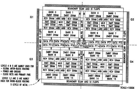
We shall accordingly first proceed to describe that layout and then to discuss
the
operational features. Along the four sides of the preferably square chip are
shown the
arrays of connector pins to the various "boundary scan and UO Fiops", so
labeled, for
connecting the chip with the network system in conventional fashion. A
plurality of 16
UO data ports ("DATA PT") is exemplarily shown along each arm of the vertical
and
horizontal cross dividing the square into four equal quadrants Q1-Q4. The
numbers of
these ports are not consecutive for reasons later explained, but each port,
however, is to
be connected to the before-mentioned corresponding SRAM transmit/receive
buffer
banla ("XMIT SRAM", "RCV SCRAM"- - also 16 in number in this illustration)
CA 02348983 2001-04-26
WO 00/26917 PCT/IB99/01732
operable under arbitration units ("ARB") to access pluralities of the
internally cached
DRAM banks ("Banks O-15") via internal busses (schematically represented at
"B" ) to
enable switching data connections amongst all data ports through the
appropriate buffers,
as earlier noted.
The upper chip surface is one of a plurality (say, five) of stacked
substantially
square conducting surfaces (such as metal plate surfaces), upon the upper
surface of
which the DRAM banks, data ports, SRAM buffer banks and arbitration units are
mounted, and along which the before-mentioned outer peripheral edge connector
pins
are positioned. Each DRAM bank (shown as of "2Mbit") is provided with its own
transmit/receive SRAM buffer bank and positioned, as shown, closely adjacent
with
respect thereto to allow the shortest length for communication with its buffer
bank busses
(256 bits). Half of the DRAM banks are distributed in spaced symmetrical rows
in the
upper half of the upper or outer chip surface (Banks 0-3 at the top row and 4-
7 below),
and the other half of the DRAM banks (8-11 and 12-I S) are distributed in
symmetrical
rows in the lower half of the upper part of the chip. With the data ports
being positioned
along the vertical-horizontal cross arms dividing the chip surface into
symmetrical
quadrants, as before described, each quadrant of the DRAM contains two half -
rows of 4
DRAMS. Quadrant Q,, for example, contains DRAM Banks 0 and 1 in the top row;
and
Banks 4 and S in the lower row. The receive and transmit SRAM buffer banks of
each
DRAM are located in the space between the DRAM half - rows in each quadrant,
such
that the buffer banks of the DRAMS in the adjacent rows are immediately
adjacent one
another. An arbitration unit ("ARB") is positioned adjacent each receive SRAM
buffer
CA 02348983 2001-04-26
WO 00/26917 PCT/1899/01732
6
bank for each DRAM, and contiguous with the arbitration unit of the ne~.-t
DRAM in each
row, with the data ports substantially symmetrically placed, and with each
data port
connected to each arbitration unit and each transmit/receive buffer bank as
described in
said Chatter documents. Each data port is thus enabled to write into any DRAM
bank,
with the connections being effected such that each data port is substantially
physically
symmetric with respect to DRAM bank, arbitration unit and transmit/receive
buffer banks
and busses. Timing clocks ("Clk") are centrally placed to minimize clock skew
by
symmetric clock distribution. A central CPU port is also provided, so-labeled,
symmetric
with respect to the DRAM banks, arbitration units and transmit/receive buffer
banks.
Repeater buffers R are also inserted centrally to achieve substantially
symmetrical data
transfer for the longer connections, as later more fully discussed.
The CPU port provides a diagnostic and control feature in this chip, whereby
the
control processor can examine the buffers and the status of each DRA1~1 bank;
i.e. where
the data is, etc. - - in short, providing a two-way communication window into
the chip.
Placing the CPU port right in the middle of the chip, moreover, guarantees
that it has
symmetric access to all the data. Pad transfer wires (such as C4 package pads)
for
achieving connectivity at the chip package level are also positioned centrally
(shown as
"pads").
An example of operation, as fully explained in the referenced Chatter
documents,
may involve sending data in, say, dataport 0 ("DATA PTO"), intended for DRAM
"Bank
14" at the lower right of the chip in the drawing to the receiver SRAM ("RCV
SRAM")
right at the top of DRAM Bank 14, and into an allocated slot reserved for
dataport 0.
CA 02348983 2001-04-26
WO 00/26917 PCT/IB99/01732
7
Each dataport, indeed, is connected to each receive SRAM where there is a
reserved
location for each dataport - - 17 slots, one dedicated for each of the 16
dataports and one
dedicated to the CPU port. This affords each data port the capability to write
into any
DRAM bank, with arbitration - - the gatekeeper - - determining which one of
these ports
enters the DRAM bank in the next~time slot. The data may go from the receiver
SRAM
into the DRAM in one shot into 256 bit wide busses, with the very short-
distance
adjacent positioning of the receiver SRAM and its DRAM bank on the chip
enabling the
choice of the 256 bit wide busses very close to the respective DRAM bank. In
the ocher
direction, when taking data out of the DRAM bank, the data goes first to the
transmitter
SRAM ("XMIT SRAM") placed immediately adjacent that DRAM bank, with the short
connection obviating any data meandering through the chip.
There is also provision, as explained in the previously referenced Chatter
documents, for partial use of the 256 byte bus, not wasting memory. At any
given
instance, however, for this example, there can be 256 x l6 (number of banks)
switching,
and each transmitting data into a 256 bit bus; all switching independently of
on;. other,
and giving rise to the very high speed of switching described in said patent.
Considering chip sizes of roughly, say, 16x16 millimeters, there are
connection
paths of varying lengths. From Bank 0 to dataport 0 therebelow ("DATA PTO"),
there is
a much shorter connection path length than to data port I S ("DATA PT 1 S") at
the far
right. As before mentioned, repeater buffers R are accordingly provided,
positioned, in
accordance with the chip layout philosophy of the present invention, near the
middle of
the chip to boost the data signal before it gets to its final destination, and
thereby
CA 02348983 2001-04-26
WO 00/26917 PCT/IB99/01732
8
achieving more substantially symmetrical data transfer for the longer
connections. There
is thus a range within which the terms symmetry or "symmetric", as herein
used, applies,
all such requiring signal completion, however, within a clock cycle.
With the clocks ("Clk") positioned in the middle of the chip in accordance
with
the invention, as before noted, symmetric clocking distances are also
achieved. Local
interconnections are mainly accomplished in two surface layers (1,2) of metal
in the
stacked chip block assembly, (schematically so-labeled in the drawing), with
all
interconnections required within the block (internal) taken to terminal
accessibility, and
which are interconnected locally with the components oo the upper chip layer,
as by well
known techniques. At the global level, three metal surface layers (3, 4 ,5),
mainly the
fourth and fifth layers, are available to make the longer wire hookup or
connections. The
fifth layer of metal, (5), is convenient for the clock routing and ground
connections.
Summarizing the chip physical layout and design of the present invention for
realizing the intended Chatter architecture with available semiconductor
technologies, the
following are the features of the design, of the technology, and of the
floorplan features
and decisions as previously discussed:
Features of the design of the invention:
1. Each dataport is symmetric with respect to the DRAM bank, arbiter and
xmit/receive buffer banks.
2. The CPU port is symmetric with respect to the DRAM bank, arbiter and
xmit/receive buffer banks.
CA 02348983 2001-04-26
WO 00/26917 PCT/IB99/01732
9
3. Each dataport is connected to each arbiter and each of the xmit/receive
buffer
banks of the system.
4. Each dataport can write into any DRAM bank.
5. Each DRAM bank communicates with its own xmit/receive buffer bank 256 bit
wide busses.
Features of the technologyi
1. The DRAM macros can not be rotated. They can be flipped.
2. 5 metal surfaces or layers are assembled in a stack for the chip block with
enabling local and global routing availability.
3. Long metal lines with lengths of 10-12 mm will have high RC drops.
4. C4 package pads need pad transfer wires to achieve connectivity at package
level.
Floorplan features and decisions:
1. Combination ofDRAM bank with its own
a) xmit/receive~buffer bank, allowing shortest length for 256 bit
busses
b) Arbiter
2. Symmetric placement of dataports
3. Symmetric placement of repeater buffers R for the long lines
4. Central placement of CPU port
S. Central placement of clocks Clk to maintain clock skew by symmetric clock
distribution
6. Routing of individual blocks in mainly metal layers 1 and 2 and 3
7. Metal layers 4 and S reserved for global routing
CA 02348983 2001-04-26
WO 00/26917 PCT/IB99/01732
8. Metal layer 5 also used for power and ground, clocks and pad transfer
traces
9. Power and ground balls of the package fully utilized for robust power and
ground
distribution by the 5'" layer of metal
While the invention has been described in terms of the chip design layout for
the
preferred internally cached DRAM switching system, it is to be understood that
its
features may also be useful for layout and operating of related networked
switching and
similar systems, as well, where the same advantages or some of them, are
desired; also,
that the illustrative values of numbers of banks, dataports, etc. and of high-
freduency
switching values, while presently preferred, are illustrative only, and may be
scaled
upward or downward, as desired; and such and other modifications as will occur
to those
skilled in this art are considered to fall within the spirit and scope of the
invention as
defined in the appended claims.