Note: Descriptions are shown in the official language in which they were submitted.
CA 02349028 2001-05-28
' X613 230 8821 MARES AND CLERK 05128101 lfi:l9 P,0051011
fr~.tEgrated Double Pass De~nultiplexer/ variable C7pHc:a1 Attenuator fc~r
channel
etluxiization
Bark~~;round o~ the Ynventinn
1. Field of the Ir~.~rention
This invention relates to the field ofphotonics, and more particularly to an
integrated double pas$ deix,ultiplexer/ variable optical attenuator ~c~r
channel
equalization.
2. Description of pelated Art
In an optical telecor~nxnunications network based on wavelength division
rnaltipiexing (4VD11~, the net optical lQSS ox gaixt between axiy two points
in the
system. often varies from orte ~ravelength channel to th,~; next. This
eharutel
dependent lass nr gain may arise from wavelength dep~,ndc:n,t annplifier gain
or
pasaiVe sources vF wavelesigtlt dependent lc~ss_ Channel dependent Ross yr
gain
can be a serious problem, paz~ticttlarly when multiple sections with similar
lt>.ss/gafn are cascac-led so that certain channels are successively amplified
to
unacceptably high :levels while others get lost in the background noxse_
If possible, the source of the wavelength dependent lass or gaits can be
eliminated, for example by employ,'.ng gain flattened crlbium doped fibre
arnplifiexs. However, wavelength variations in loss or gain oar< never be
entirely
2Q eliminated From the system. 'i'liereFore some form of spet~tral flattening
must be
used.
Spectral Flattering or channel equalization can be aehuQ~red ~,y passive
filters wzth
a, wavelength dependent trartsmissic~n. Unfortunately passive devices cazunot
adjust to dynamically changizxg conditions in the systez~~,_ ,A,ckive ehamcl
e~oal.ization can be parried out using a variable optical attenuator (v~A) xn
combination with a wavelength dernultiplexer. The detnultipltxer separates out
each wavelength t~hannel, and a separate v~,v4 is used to attenuate the each
sil;nal by a Factor such that the Final output indensities o:F all ~hanne]s
ace the
same_ After the vOA, a mt~ltiplexer must be used in ord'.er to recombine all
the
CA 02349028 2001-05-28
X613 230 8821 hf>1RKS AND CLERK OS128l01 1fi:20 P,OOfi1011
..
channels back into a single output Fibre. A ntimbex of schemes exist for
carrying
ouk this function, all of which require the combination of discrete
demultiplexers,
VOAs and znultiplexers. Another prerequisite for any ~;ueh system is the use
of a
channel znoW tot. The channel monitor measL~es the intensity of every channel
and provides the necessary feedback to the VOA to ertstue that all channel
intensities az~e attenuated correctly.
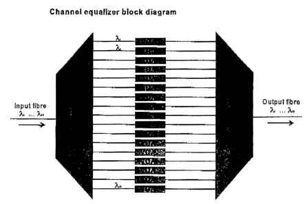
The active channel equalization schemes all rely on the a$sembly Qf discrete
demultiglexers, VOAs, arid rnultiplexers. A simple 16-c:haru~el equalizer,
shown
in block diagirarm form in Figure I, requires a d~nnulti~plLexer,
rntQtiplexer, and 15
1Q VQAs, and will ittvolwe at least ~6 separate fibre junetic~ns_ As a result
assembly
will be the most in.~portant factor driving the package cost up, and assembly
and
packaging defects will be the most important factor in decreasing
rnanu"facturing
yield. VOA devices ge~nez~al.ly require a certain power input irx ozder to
operate,
particularly those based on thez~mcroptic and carriee injection effects. ;~oz
WDM
systems with many channels, each wavelength channel rni~st have it's own
independent VOA. The result is khat tha system power consumption and
dissipation can become quite large. This cars. be a problem both in terms oi'
the
cost and eduipmeant required to supply that Bower, andl in the removal of the
dissipated heat at both the individual ron~ponent and rack le~rel.
8uxnmary of the Invention
This invention describes a method for combining an optical planar waveguide
clemultiplexer, wa~re~uxde mirrors and waveg,~.ide variable optical.
attanuators
(VOA) on a single znonoliEhi.c chip. The resulting integrated device requires
only
one input/QUtput fibre. This invention can be used as a channel equalizer in
WnM systerns_
In a broad aspect, the invention uses a double pass configuration for a
channel
equalizer based on art inEegrated variable optical atkenustor (VOA) and a
tlemultiplexer.
CA 02349028 2001-05-28
X613 230 8821 BARES IfND CLERK 05128101 16:20 P,00~lOil
Bxi~ef Descri.ptiorx of the Drawrings
'lhe invention krill now be described in more detail; by ~r~ay of example,
only ~ritl~
reference to the accompanying drawings, in wlicln:-
Figure 1 is a block di~~~gram of a channel equalizer block; and
Figure 2 illustrates a double pass deniuliplexerf ~rariable~ optical
attez~uator.
T~etailed Desrcaption of the In~rention
In accordance with the pri;,ciples of the inv~entaon, a double pass
config<iration for
a ehar<nel equalizer based on an integratxd VQA and demitltiplexer. A
schematic
diagram of the proposed device is shown in Figc,re 2_
IO .1n Figure 2, an optical signal consisting of many different waveleny-th
cha~,nels is
directed to the chip by an optical ci:rcula for A. The light ~i,~ coupled from
the fibre to
the input guide B_ The component channels are separated out and directed into
corr~s~ponding VOA waveguides D icy an echelle gratin; ~_ Each output guide is
cot,~pled to E, a waveguade lrOA. Finally the Light exits tha VQA section anal
sfrikes
'15 a mirror F t(~st returns the beam back through the VOA and demultiplQxer.
Since
the beam paths axe precisely reversed, all channels will Ire recombined onto
the
input guide of the den.,ultiplexer and into the fibre. The optical rircuXator
then
directs the attenuated channels d.owostream from the signal source.
The advantages of this eor~Cguratioz~ are:
20 1. Deduction of required assembly. There is only once ,fibre to waveguide
junction required, fox sr~y ntmnber of chanrtels_ This will :Lead to an
eno,snn4us
reduction in assembled device cast. A separate optical circulator is required
to
separate the up a.nd. downstream path;;, bu t connectorized circulators a re
readily
available with very goad p~r~oxainanee at a small relative cost.
2a 2. Reduction in package footprint. Since there is no internal fibre to
waveguide
coupling and ~,o i~ntetnal fibt~ ismgth~, tl,~ szze of the packaged device
should be
much smaller than a similar channel equalizer composed of discrete components.
-3-
CA 02349028 2001-05-28
' x'613 230 8821 MARKS AND CLEPK 00128101 16:20 P,008I011
a
3. Reduction in VOA power or voltage recluiremer<~ts_ Since each char~n~l
passes through the VUA twice, the power (or voltage bt the ease of ~lo~t~ro-
optic or
electrostatic l~lViS VOAs) required to ar"hieve a given attenuation is half
tl~.at
required in conventional demultiplexer VOA assexnblie:>.
The kty technologies reqLZired are-_
1_ A wav~g,,dde based demultiplexer. Either an echelle grating based device,
or an arrayed waveguide ,grating (AWG) device can be used. 'The eehelle
i
demuitiplexer is preferred since the derrtultiplexer fac~tprint is ~cx~uct~
smaller than
that fur an AWG.
x ~ 2. A waveguide VOA. 'r'he VOA can be based on a xW mbec of mechanisms.
For example, if a silicon-on-insulator (SC)!) or other semicond~ucCor
wavegcdde
platform is used for the chip, a carrier injection or electra-optic V(~A can
be used.
In the Case of glass and/or polymer waveguide chip, the VOA rnrill. likely be
a
thermo-optic device. MEMS based Vt7As may also be a Ixyssibility.
15 3. Waveguide pnirrors. The m,ixxors will require vertical ~t~l~~s (to
within one
degree or leas) in the materiswl system used_ f~igh refl~cti~u~ity can be
achieved using
metal or znultitayer dielectzic coatin,gs_ Tn the case of high refractive
index
wa~r~guides such as SOI, silicon axynatride or rn~;a,g,sP, high rrfleetivity
can be
achieved by terminating the wavegu.ides with, right angle cvrrser reflectors.
Total
20 iu~ernal reflection at the ~clraveguid~ /air interface should in theory
,give 100%
re~le~tiwi~ty.
-4-