Some of the information on this Web page has been provided by external sources. The Government of Canada is not responsible for the accuracy, reliability or currency of the information supplied by external sources. Users wishing to rely upon this information should consult directly with the source of the information. Content provided by external sources is not subject to official languages, privacy and accessibility requirements.
Any discrepancies in the text and image of the Claims and Abstract are due to differing posting times. Text of the Claims and Abstract are posted:
| (12) Patent Application: | (11) CA 2349033 |
|---|---|
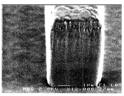
| (54) English Title: | INITIAL PLASMA TREATMENT FOR VERTICAL DRY ETCHING OF SIO2 |
| (54) French Title: | TRAITEMENT A L'AIDE D'UN PLASMA AVANT LA GRAVURE A SEC VERTICALE DE SIO2 |
| Status: | Dead |
| (51) International Patent Classification (IPC): |
|
|---|---|
| (72) Inventors : |
|
| (73) Owners : |
|
| (71) Applicants : |
|
| (74) Agent: | MARKS & CLERK |
| (74) Associate agent: | |
| (45) Issued: | |
| (22) Filed Date: | 2001-05-28 |
| (41) Open to Public Inspection: | 2002-11-28 |
| Availability of licence: | N/A |
| (25) Language of filing: | English |
| Patent Cooperation Treaty (PCT): | No |
|---|
| (30) Application Priority Data: | None |
|---|
Note: Claims are shown in the official language in which they were submitted.
Note: Descriptions are shown in the official language in which they were submitted.
For a clearer understanding of the status of the application/patent presented on this page, the site Disclaimer , as well as the definitions for Patent , Administrative Status , Maintenance Fee and Payment History should be consulted.
| Title | Date |
|---|---|
| Forecasted Issue Date | Unavailable |
| (22) Filed | 2001-05-28 |
| (41) Open to Public Inspection | 2002-11-28 |
| Dead Application | 2003-08-29 |
| Abandonment Date | Reason | Reinstatement Date |
|---|---|---|
| 2002-08-29 | FAILURE TO RESPOND TO OFFICE LETTER | |
| 2003-05-28 | FAILURE TO PAY APPLICATION MAINTENANCE FEE |
| Fee Type | Anniversary Year | Due Date | Amount Paid | Paid Date |
|---|---|---|---|---|
| Application Fee | $150.00 | 2001-05-28 |
Note: Records showing the ownership history in alphabetical order.
| Current Owners on Record |
|---|
| LAMONTAGNE, BORIS |
| RENDER, WILLIAM |
| Past Owners on Record |
|---|
| None |

