Note: Descriptions are shown in the official language in which they were submitted.
CA 02349282 2001-05-03
WO 00/25854 PCT/US99/25814
TITLE OF THE INVENTION
A HIGH IMPEDANCE, LOW POLARIZATION CARDIAC ELECTRODE
BACKGROUND OF THE INVENTION
Field of Invention
This invention relates to implantable electrodes and more particularly to a
cardiac
pacing lead distal tip electrode.
Description of Related Art
Pacemaker leads are used to electrically connect a cardiac pacemaker pulse
generator to heart tissue to be stimulated. For example, endocardial type
leads which are
inserted into a vein and then guided into the desired heart cavity include at
their distal end
an electrode tip designed to contact the endocardium or the tissue forming the
inner lining of
the heart. These leads, connected to a pacemaker, are commonly used for both
sensing
electrical signals produced by the heart and providing pacing stimulation.
The electrical pacing signal that is delivered to the cardiac muscle must be
of
sufficient magnitude to depolarize the excitable cells that are adjacent to
the electrode tip.
The electrode size and shape, tissue conductivity, and the distance separating
the electrode
tip from the excitable cells are factors in determining the stimulus
threshold. Many of these
factors are highly determined by the geometry and material composition of the
electrode.
The duration or battery life of a pacemaker is, in part, dependent on the
current drain
that is used in stimulating the cardiac muscle. This current drain is
determined by the
programmed voltage, pulse width, the rate of the pacemaker stimulator and the
pacing
impedance presented to the pulse generator. It is important to note that
improvements in
pacemaker longevity due to increased pacing impedance are not dependent upon
reprogramming the pacemaker in any manner.
The pacing impedance is a function of the macroscopic surface area of the
electrode. As it is optimal to have a high pacing impedance, most modern
pacing electrode
designs strive for a reduced area stimulus electrode. Thus, small diameter
electrodes will
reduce the stimulus current necessary to pace the heart and will extend the
life of the
pacemaker. Electrodes having very small tip surface areas, in some designs,
are
problematic in that the small surface area or sharp point can increase the
chance of the
CA 02349282 2001-05-03
WO 00/25854 PCT/US99/25814
electrode perforating the ventricular wall, which can lead to blood loss into
the pericardial'
sack. In addition, small tip electrodes are also very sensitive to
implantation angle and can
demonstrate marked stimulus threshold variability during occurrences of lead
micro-
dislodgement due to the very uneven surface structure of the endocardial wall.
At times the
sensitivity to stimulus threshold with micro-dislodgment can cause exit block
or complete
loss of cardiac stimulation.
It should also be noted that electrodes having very small stimulus areas are
prone to
generate large polarization artifact signals. These voltage signal distortions
are inefficient in
that they take energy away from stimulation of the cardiac tissue. More
importantly, these
artifact signals can present problems to the pacemaker in sensing the
following heart
activity. One method to reduce this artifact is to increase the microscopic
surface area of
the electrode, while keeping the macroscopic surface area fixed. This
microscopic surface
area is the sum of all the microscopic cracks, crevices and indentations on
the surtace of
the electrode.
The electrode must also provide a means for sensing the electrical activity or
signal
of the heart. The ability to efficiently detect heart activity is directly
related to the sensing
impedance of the electrode. Optimal sensing occurs with low sensing source
impedance
electrode designs. Thus large macroscopic surface area electrodes are desired
for sensing.
The pacing, or stimulating, threshold is a measurement of the energy required
for a
voltage pulse to initiate a contraction in the heart tissue. The stimulus
threshold typically
rises after implantation of an electrode since there is an increase in the
spacing between the
electrode tip and the excitable cardiac tissue. This is a typical foreign body
tissue healing
response to the electrode tip and this healing response includes the
generation of a fibrous
capsule around the electrode tip. Lower stimulus thresholds have resulted from
electrode
designs with a porous structure at the distal electrode end. Optimal porous
structures
appear to minimize the initial foreign body reaction and hasten the subsequent
healing
response to the pacemaker lead tip electrode.
Thus, a considerable design challenge in current state-of-the-art electrodes
is the
optimization of the electrode surface area, geometry and porosity. High pacing
impedance
is optimally achieved by low macroscopic surface area electrode geometry. Low
polarization losses are optimally achieved by a high microscopic surface area
electrode
geometry. Low sensing source impedance requires large macroscopic surface area
electrode geometry. Low sensitivity to micro-dislodgement requires large
macroscopic
surtace area electrode geometry. The design outcome is always a compromise
between
2
CA 02349282 2001-05-03
WO 00/25854 PCT/US99/25814
the opposite desired extremes. Recent devices utilize various types of surface
coatings or
metal surface enhancements (e.g., iridium oxide). These surface changes
increase the
microscopic surface area while keeping the electrode macroscopic surface area
relatively
the same. These surface enhancements help reduce the polarization losses for a
given tip
geometry but do not fully solve the design tradeoff concerns on the electrode
surface.
An electrode tip design, taught in US Patent 3,476,116 by Parsonnet et al.,
utilizes
an electrode tip with a fluid filled cavity. Within this cavity is a high
surface area electrode.
The fluid filled cavity is isolated from the tissue to be stimulated by an
electrically insulating
material containing a small aperture. This electrode tip design has, in
effect, a large
electrode surface area which lowers the polarization losses. The tissue to be
stimulated
however perceives a very small surface area due to the small aperture,
resulting in high tip
to tissue impedance. This design performed reasonably well short term, however
the long
term or chronic performance was shown to be compromised. The small aperture of
the
Parsonnet design was highly sensitive to lead movement due to micro-
dislodgment which
changed the interface between the tissue and the small aperture. This aperture
dislodgment
caused high stimulation voltage thresholds in some patients and in extreme
cases caused
total electrode exit block which is a complete failure to stimulate.
A modified Parsonnet design was disclosed by F. Hoffmann in an article
entitled
"Stimulating Electrode With Low Energy Consumption" (Medical and Biological
Engineering,
September 1973, Pg. 659-660). This proposed design added additional holes or
apertures
to the original Parsonnet design. The sensitivity of the tip to tissue
interface was effectively
reduced, however consistent and stable chronic pacing thresholds were still
not obtained.
A similar electrode tip design is disclosed in US Patent 5,282,844 to Stokes
et al. To
achieve low polarization losses, Stokes et al. teach the use of a fluid filled
cavity containing
an electrode with a large surface area, similar to that of Parsonnet et al.
Low stimulation
voltage thresholds are achieved by the use of a cavity sheath with a small
aperture, again
similar to the Parsonnet design. To overcome the chronic increase in
stimulation voltage,
the Stokes design incorporates a steroid eluting device contained within the
bodily fluid filled
cavity. The steroid elution alters the results of the reaction to the foreign
body response at
the electrode tip to tissue interface and results in low chronic stimulation
voltage thresholds.
In US Patent 4,011,861, Enger teaches the use of an electric terminal, with a
porous
outer sheath. The porous sheath encourages the ingress of blood vessels
without the
production of a fibrous tissue interface which would result in high
stimulation voltages. The
3
CA 02349282 2001-05-03
WO 00/25854 PCT/US99/25814
large number of pores result in a large number of sites of current loss with
no areas of high
current density nor a marked increase in stimulus pacing impedance.
MacGregor teaches in US Patent 4,281,669 a high surface area, sintered metal
electrode tip, incorporating an outer porous polymeric covering. The pores
provide for an
improved tissue ingrowth structure at the tip. The high surface area sintered
metal
electrode provides low polarization losses. Similar to Enger, the large number
of pores of
MacGregor result in no areas of high current density for stimulation.
In US Patent 5,090,422 to Dahl et al., an electrode sheath is disclosed. Dahl
et al.
teach the use of a porous polymeric sheath, which when impregnated with bodily
fluids,
becomes electrically conductive. US Patent 5,609,622 to Bush also discloses a
porous
polymeric sheath. This polymeric sheath has a pore size of less than 10
microns for the
purpose of precluding tissue attachment which facilitates removal of the lead
after chronic
implantation. The porosity also allows bodily fluids to impregnate the sheath
thereby
allowing electrical energy to pass through the sheath. The porous polymeric
sheaths
disclosed in Dahl et al. and Bush result in a large number of very small sites
of current loss
with no areas of high current density nor a marked increase in stimulus pacing
impedance.
SUMMARY OF THE INVENTION
The present invention provides a layered electrode having an electrically
conductive
material, covered by one or more layers, wherein the electrode provides high
pacing
impedance, a low chronic stimulation voltage threshold and low post pacing
polarization
artifacts. Specifically, the present invention is an electrode comprising an
electrically
conductive material which is covered or substantially covered by a layer of
substantially
electrically insulating material having at least one macroporous perforation
(or aperture)
therethrough, and a microporous cover over the perforation. The at least one
macroscopic
perforation provides a high current density path while the microporous cover
is permeable to
electrically conductive body fluids which allow current to flow through the
cover. Preferably
the microporous cover simultaneously prevents tissue ingrowth into the at
least one
perforation.
In a preferred embodiment, the microporous layer is provided as two layers in
the
form of an external microporous layer having a pore size appropriate to
promote tissue
attachment to that layer by allowing tissue to grow into the pores of that
layer, and an inner
cell exclusion layer with pores adequately small to restrict or entirely
prevent cell ingrowth.
4
CA 02349282 2001-05-03
WO 00/25854 PCT/US99/25814
Both layers together are permeable to body fluids. In another preferred
embodiment which
may be used with either the single or two layer microporous cover, the
electrically
conductive material of the electrode is in the form of an electrically
conductive component
provided with a surface of large area such as a porous metal, powdered metal,
sintered
metal, or any other means of enhancing the surface area of the electrically
conductive
component in order to enhance the charge transfer between the electrically
conductive
component and electrically conductive body fluids. The means of enhancing
surface area of
the electrically conductive material may involve the addition of one or more
layers to the
surface of the electrically conductive material.
1 o These multiple layers, in concert, can provide good biocompatibifity,
electrode tip
anchoring to the tissue to be stimulated, prevention of cell proliferation
into the subsequent
layers, one or more localized high current density stimulation sites, a high
pacing impedance
due to an effectively small macroscopic surface area electrode, and a low post
pacing
polarization artifact.
BRIEF DESCRIPTION OF THE DRAWINGS
These and other objects and advantages of the present invention may be fully
understood and appreciated in conjunction with the attached drawings and
following detailed
descriptions.
Figure 1 shows an overall view of a pacing lead and stimulation system of the
present
invention.
Figure 2 shows a longitudinal cross section of the multiple layered distal
electrode of the
present invention.
Figure 2A shows a longitudinal cross section describing a preferred embodiment
of Figure 2
having additional layers.
Figure 3 shows a detailed cross section of the sequenced multiple layers of
the distal tip of
the present invention.
5
CA 02349282 2001-05-03
WO 00/25854 PCT/US99/25814
Figure 3A shows a detailed cross section of sequenced layers in an alternative
embodiment
of the distal tip of the present invention.
Figure 4A shows a perspective view of the third, pertorated layer of the
distal electrode, the
layer having at least one aperture therethrough.
Figures 4B through 4G show end and side views of various hole or perforation
patterns in
the electrically insulating layer.
Figures 5 and 6 are cross-sections describing a method of assembling the multi-
layer distal
electrode.
Figure 7 is a graph showing the relation of threshold voltage vs. pulse width,
at 35 days post
implantation.
Figure 8 is a schematic drawing of the test apparatus used for determining the
electrode
impedance and the post pacing polarization artifact.
DETAILED DESCRIPTION OF THE DRAWINGS
The present invention is an electrode comprising a layered tip which provides
a
chronic electrode to tissue impedance of greater than about 1000 ohms and
maintains a
chronic stimulation voltage of less than about 5.0 volts without the use of
steroid elution. In
a preferred embodiment, the present invention is a multiple layered device
comprising, in
sequence, a) an external layer promoting tissue attachment, b) a secondary
cell exclusion
layer, which prevents tissue ingrowth into the subsequent layers, while
allowing passage of
conductive fluids, c) a third layer of substantially electrical insulating
material with selected
or tailored perforations, apertures or through holes which provide high
current density paths,
d) a fourth layer that contains a electrically conductive material of high
surface area and e) a
fifth metallic layer having a high surface area. "Comprising in sequence" is
hereby defined
as a specific order or arrangement of the layers but does not preclude the use
of additional
intermediate layers. Thus, for example, the tissue attachment layer may be
physically
separated from the cell exclusion layer by a mesh material. The addition of
this mesh, or
6
CA 02349282 2001-05-03
WO 00/25854 PCT/US99/25814
intermediate layer, therefore does not preclude the tissue attachment layer
from being in
sequence with the cell exclusion layer. The term "cover" is hereby defined as
a surtace or
material which, at least partially, overlays, envelops, coats or otherwise
covers an
underlying or internal surface or material. Similar to the above definition of
"comprising in
sequence", an internal surface or material is considered covered, despite the
presence of
any additional surface or materials between the cover and the internal covered
surface or
material. To be considered covered, an internal surface or material does not
have to be in
direct contact with the cover. For example, intermediate layers or surfaces
may exist
between the covered surface and the cover.
A unipolar pacing lead, as generally described previously, is an implantable
insulated
electrical wire terminating in a distally located electrode. The electrical
current path is
composed of both conduction through the pacing lead electrical wire which is
considered
electronic flow (the flow of electrons) and conduction through the blood and
other body fluids
which is considered ionic flow (the flow of ions). The transition from
electronic conduction to
ionic conduction requires a charge transfer across the electrode surface
interface. The
surface of the electrode is therefore the physical area or interface where
such a charge
transfer occurs.
Figure 1 is a plane view of a typical implantable pacing lead 2. The pacing
lead 2
has a proximal end 4, configured to connect to a pacing generator, or
stimulator 3 and a
distal electrode 6 for stimulation of bodily tissue. The implantable lead 2
and the stimulator
3, comprise a stimulation system.
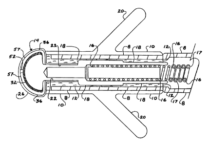
Figure 2 is a longitudinal cross section of the distal electrode 6. The coiled
electrical
conductor 16 is electrically connected to the base electrode 18. The coiled
electrical
conductor 16 is contained within an outer sheath 8. Electrical isolation is,
in a preferred
embodiment, achieved by coating the coiled wire 16 with an electrically
insulating coating
17, for example ethylene - tetrafluoroethylene (ETFE). At the extreme distal
end, the outer
sheath 8 is covered by anchoring tine component 10 which incorporates
anchoring tines 20.
The outer sheath 8 is attached to the base electrode 18 by a bonding agent 12.
The same
bonding agent 12 is used to attach the multiple layers of the distal electrode
assembly 14 to
3o the base electrode 18. The outer sheath 8 can be fabricated from any
suitable
biocompatible material, for example, polyurethanes, silicones or in a
preferred embodiment
porous polytetrafluoroethylene. The bonding agent 12 can be any suitable
biocompatible
material such as silicone or in a preferred embodiment fluorinated ethylene
propylene
(FEP). A suitable form of FEP is available from Norton Pertormance Plastics,
Wayne NJ, as
CA 02349282 2003-05-08
WO 00/25854 PCT/US99/25814
Korton~ FEP Fluoropolymer Film. The base electrode 18 can have ridges, barbs,
grooves or
a suitable rough exterior surface finish to enhance the adherence of the
bonding agent 12.
Similarly, the multiple layers bf the distal electrode tip assembly 14 can be
configured with
appropriately roughened surfaces to increase the adhesive bond strength in the
layer to
base electrode attachment area 22.
As further shown in Figure 2, the distal electrode tip of base electrode may
be
provided with a means for more effective electrical charge transfer in the
form of a high
surface area coating 32 such as a powdered or sintered metal coating or a
coating of other
porous or roughened metal. Layer 36 in the form of a perforated sheet of
substantially
' electrically insulating material covers the high surface area coating 32 of
the distal electrode
tip of base electrode 18. This perforated layer 36, provided with at least one
perforation or
aperture 52 therethrough surrounded by substantially electrically insulating
material 57, is in
turn covered by microporous layer 26 which is permeable to electrically
conductive body
fluids. Aperture 52 provides a localized, high density current path through
perforated layer
36.
Perforated layer 3fi may simply be captured or contained by an external
microporous
layer 26, thus a perforated layer 36 does not necessarily have to be directly
bonded to the
base electrode 18. Multiple layers of the distal electrode tip assembly can be
contained in
such a fashion.
Shown in the longitudinal cross section of Figure 2A and in greater detail in
the
enlarged longitudinal cross section of Figure 3 is a description of the
multiple layer distal
electrode assembly 14, wherein wherein the electrically conductive material of
base
electrode 18 is provided with enhanced surface area by a coating of sintered
metal 32 and
an additional layer of carbon-filled ePTFE 34. This assembly is then covered
with a layer 36
of substantially electrically insulating material having at feast one
perforation therethough,
which is in~turn covered by body fluid permeable, microporous layers 38 and 40
wherein
layer 38 is a cell exclusion layer and layer 40 is a cell ingrowth layer.
As noted above, the base metallic electrode 18 preferably has an external,
selective
surface coated with high surtace area sintered metal 32. The base metallic
electrode 18
can be fabricated from any suitable biocompatible electrically conductive
material, or
conductive metal element, such as 90%110% Ptllr. The high surface area
sintered metal 32
can consist of any conductive biocompatible material having a suitably high
surface area.
Typical sintered materials 32 include 90%110% Ptllr alloy micro spheres,
approximately 20-
50 microns in diameter, coated onto the base electrode 18 by conventional
means.
CA 02349282 2003-05-08
WO 00/25854 PCT/US99r.
Adjacent to the high surface area coating 32 is an electrically conductive
material, or
carbonized polymer, which in a preferred embodiment is a carbon filled ePTFE
layer 34.
Thus lajler 34 comprises an electrically conductive polymer material. This
carbon filled
ePTFE layer 34 enhances the transfer of electron current flow in the coiled
conductor, to
ionic current flow of bodily fluids. The high efficiency is a result of the
high microscopic
surface area of the carbon filled ePTFE in contact with bodily fluids. This
carbon
filled layer or material is produced in accordance with U.S. Patent 5,560,986
to
Mortimer. In a preferred embodiment, this carbon-filled material is produced
following example #1 .of the aforementioned patent, with the following
exceptions:
90 1) the tape was calendered through heated rolls to 0.14 mm vs. 0.28 mm, 2)
the tape was,
stretched in the machine direction once vs. twice, with an expansion ratio of
2.5 to one, 3)
the expanded tape was then not compressed vs. being compressed. The high
surface area
of the combined carbon filled layer 34 atong with the high surface area of the
sintered metal
base electrode coating 32, result in low current densities and low
polarization losses.
As shown in Figure 3, a third layer or cover 36 covers the electrically
conductive
polymer material or the carbon filled ePTFE layer 34. The third layer 36 is
fabricated from
any suitable biocompatible, substantially electrically insulating material,
and is provided with
at least one aperture 52 therethPough. In a preferred embodiment layer 38 is
FEP with
multiple through holes, forming a specific array or pattern of perforations or
apertures. This
2o third layer 36, covers and electrically isolates the carbon filled ePTFE
layer 34 from the
body, except for the current paths provided by the perforations. The precise
perforation
hole pattern is designed to result in localized areas of high current
densities and high ,
electrode pacing impedance. Specific details relating to the construction of
this electrically
insulating layer or cover are disclosed in subsequent sections. Importantly,
the electrically
insulating material of this layer is not limited to a near ideal, or high
resistance material, and
can be farmed from a substantially electrically insulating material. A
substantially electrically
insulating material is hereby defined as a material or layer, which when fully
wetted, .has an
electrical resistance at least about twenty times greater without perforations
than with
perforations. Thus the goal of the perforations is to achieve localized areas
of high, or
3o increased, current densities at the perforation sites compared to the
current densities at the
non-perforated sites. An aperture is hereby defined as a hole, perforation or
a porous area
through the thickness of a layer of substantially electrically insulating
material (i.e.,
therethrough) which covers an electrically conductive component, resulting in
a high current
density at the local site of the aperture.
9
CA 02349282 2001-05-03
WO 00/25854 PCT/US99/25814
The fourth layer or cover of the present invention serves as a cell exclusion
layer 38.
In a preferred embodiment, the cell exclusion layer 38 is formed from ePTFE
having a
specific microstructure designed to prevent cellular penetration into the
inner layers.
Cellular ingrowth into the internal layers has the possible negative effect of
degraded
electrical performance. In a preferred embodiment, the cell exclusion layer or
cover is
comprised of a thin, high strength, stretched, non-woven web of
polytetrafluoroethylene
composed substantially of fibrils in which the nodes are represented primarily
only as fibril
junctions. This layer has a mean fibril length of less than about 3.0 microns
with a preferred
range of less than about 1.0 microns and more preferably between about 0.05
and 0.4
microns. The thickness of the material is, in a preferred embodiment, between
about 1
micron and about 25 microns.
The fifth layer, cover 40, is configured to encourage cell ingrowth or
attachment to
facilitate the electrode tip anchoring and thus insure consistent chronic
electrical
characteristics. This cell ingrowth layer or cover 40 is formed, in a
preferred embodiment,
from ePTFE having a specific microstructure designed to encourage cellular
penetration.
Preferably, the materials for the cell exclusion layer 38 and the material for
the cell ingrowth
layer 40 are a laminate of at least two layers of porous
polytetrafluoroethylene materials
each having a different porosity. The lamination of these two film layers, the
process for
which will be subsequently described, facilitates the handling of the thin
films during
2o subsequent processing. Thus the lamination process is not considered to be
critical
regarding the electrode performance, and may be eliminated if deemed
unnecessary.
Figure 3A describes a detailed cross section, in similar fashion to the cross
section
of Figure 3, of an alternative embodiment of the inventive electrode tip
wherein layer 36
provided with the at least one aperture is combined with microporous layer 26
(preferably
intended to exclude cell ingrowth). This can be accomplished in different ways
with the
result being a layer 39 provided with apertures 53 which are microporous
rather than entirely
open, with the pore size of the microporous region preferably being adequately
small to
exclude cell ingrowth. Apertures 53 are surrounded by substantially
electrically insulating
material 57. Layer 39 is then preferably provided with additional covering
layer 40 which is
a microporous cell ingrowth layer. Layer 39 is provided over base electrode
18, preferred
sintered metal coating 32 and preferred conductive ePTFE layer 34.
Layer 39 may be made in various ways. One method is to select a sheet of
microporous ePTFE having the desired mean fibril length appropriate for
aperture 53 and
densify the area 57 surrounding aperture 53 by the application of pressure
until the area 57
CA 02349282 2003-07-16
w0 00/25854 PCT/US99l25814
is no longer porous. This results in area 57 being of reduced thickness in
comparison to the
aperture region 53; this reduced thickness is not anticipated to be a problem
with respect to
the function of this layer. Densification of porous ePTFE to provide selected
non-porous
regions is taught by US Patent 5,032,445 to Scantlebury et al. Alternatively,
non-porous
region 57 may be made by filling the void spaces of the porous sheet of ePTFE
with a
suitable filler such as medical.grade silicone adhesive while leaving the
aperture region 53
unfilled and still microporous; alternatively this region 57 may be provided
with a coating of a
non-porous sealant such as the silicone material. All of these methods allow
aperture 53 to
provide a localized area of high current density.
The portion of the laminate or cover containing the cell ingrowth layer 40 is
a porous
expanded polytetraffuoroethylene material (ePTFE) having a microstructure of
nodes
interconnected by fibrils, made in accordance with the teachings of U.S.
Patents 3,953,566
and 4,187,390 to Gore. These patents
teach that ePTFE maybe manufactured in a range of densities (inversely
proportional to
porosity) and pore sizes. Pore size with regard to ePTFE is most cornrnonty
characterized
in terms in mean fibril length which refers to the mean length of fibrils of
the material, or
more conveniently, the mean distance between adjacent nodes. The ePTFE
material for
use as the cell ingrowth layer has an mean fibril length greater than about
3.0 microns and
preferably greater than about 50 microns. The thickness of the material ranges
from about
10 microns to about 1000 microns, preferably about 40-60 microns.
Mean fibril length is measured as taught by US 5,747,128 at col. 6, lines 19-
37.
Mean fibril length can be estimated with adequate accuracy for most purposes
by visual
examination of SEM photomicrographs of an ePTFE sample surface by those of
ordinary
skill in the art.
The preferred method of making the cellular exclusion layer 38 of the laminate
or
cover utilizes a portion of a method taught by Bacino in U.S Patent 5,476,589
entitled
°Porous .PTFE Film And A Manufacturing Method Therefor". In the Bacino
method, after the
appropriate polytetrafluoroethylene starting materials are chosen and prepared
as a coagulated
dispersion of fine powder polytetrafluoroethylene, the coagulated dispersion
powders are lubricated
with a hydrocarbon extrusion aid, preferably as odorless mineral spirit such
as Isopar~ K (made by
Exxon. Corp.). The lubricated powder is compressed into cylinders and extruded
in a ram
extruder to form tapes. Two or more layers of tape can be stacked together and
compressed between two rolls. The.tape or tapes are compressed between rolls
to an
11
CA 02349282 2001-05-03
WO OO/Z5854 PCTNS99/25814
appropriate thickness, e.g. 5 to 40 mils, or so. The wet tape is stretched
transversely to 1.5
to 5 times its original width. The extrusion aid is driven off with heat. The
dried tape is then
expanded, or stretched, longitudinally between banks of rolls in a space
heated to a
temperature that is below the polymer melting point of 327°C. The
longitudinal expansion is
such that the ratio of speed of the second bank of rolls to the first bank is
between 10 to 1
and 100 to 1, preferably 35 to 1. The longitudinal expansion is repeated at a
ratio greater
than 1 to 1 and less than 1.5 to 1, utilizing a third set of rollers.
After the longitudinal expansion, the tape is expanded transversely at a
temperature
that is less than 327°C to at least 1.5 times and preferably to 6 to 15
times the input width of
the original extrudate while restraining the membrane from longitudinal
contraction. While
still under constraint, the membrane is preferably heated to above the polymer
melting point
of 327°C and then cooled.
Lamination of these two different porous polytetrafluoroethylene materials
(the cell
ingrowth layer and the cell exclusion layer) is performed by combining some of
the steps of
the above referenced Bacino method. To perform the lamination, the cell
ingrowth material
is joined with the material from the Bacino method between the second and
third set of rolls
and longitudinally expanded together during the above described second
longitudinal
expansion having an expansion ratio of greater than 1:1 and less than 1.5:1.
The thickness
of the laminate can be less than 55 microns.
Next the laminate or cover, after the longitudinal expansion, is expanded
transversely at a temperature that is less than 327°C to at least 1.5
times and preferably to
6 to 15 times the input width of the original laminates while restraining the
laminate from
longitudinal and transverse contraction. While still under constraint the
laminate is
preferably heated to above the polymer melting point of 327°C and then
cooled.
The construction of the perforated, substantially electrically insulating
layer 36 of
Figures 2-3 are further described in detail beginning with Figure 4A. As shown
in Figure 4A,
an initial sheet 50 of the substantially insulating material is positioned, in
a preferred
embodiment, onto a laser cutting fixture (not shown). The substantially
insulating layer 50 is
then perforated with a series of holes (apertures) 52 surrounded by
substantially electrically
insulating material 57. The initial sheet 50 has an approximate electrode
surface area
contained or defined by the periphery 54. This periphery 54 defines an initial
maximum
surface area or mechanical contact area 55 (the entire area within periphery
54), which
covers the entire macroscopic surface area of the sintered metal layer 32
(Figure 3).
Enough material 58 outside of periphery 54 must be provided for attachment of
the layer 50
12
CA 02349282 2001-05-03
WO 00/25854 PCT/US99/25814
to the electrode assembly as will be seen subsequently in Figure fi. Each hole
52, has, in a
preferred embodiment, a substantially similar hole area 56. After cutting the
holes in sheet
50, the ratio of the number of holes 52 multiplied by the typical hole area
56, to the
mechanical contact area 55 is preferably less than 0.40. This ratio is
referred to as the
perforation ratio. Devices of the present invention have typical hole,
aperture or perforation
areas 56 ranging from about 0.008 to 0.09 mm2 (corresponding to diameters of
about 0.1
mm to 0.34 mm for circular apertures) with a preferred range of 0.015 to
0.07mm2. Devices
of the present invention have a preferred number of perforations or apertures
52, ranging
from 3 to 30 (at least 3 apertures representing a "multiplicity" of
apertures), with a preferred
range of 5 to 18. By perforating the insulating sheet 50 while in the flat or
planar state, very
accurate holes can be cut, having precise hole areas, hole spacing and hole
patterns.
These high cutting accuracies are difficult to achieve when the insulating
layer is in the final
hemispherical shape as shown by assembly 14 in Figure 2. In addition, by only
exposing
the insulating layer to the cutting process, the other inner and outer layers
of the distal
electrode tip are not affected or compromised by the perforation cutting
operation.
It is important to note that following assembly onto the distal electrode, the
perforated, substantially insulating layer 36 results in an electrode with a
much higher
pacing impedance when compared to the pacing impedance from an electrode
identically
constructed but without this layer. This is a result of the perforation ratio,
as previously
defined, markedly reducing the effective area for current stimulation. The
specific
perforations are designed to result in localized areas of high current
densities and high
electrode pacing impedance. Devices of the present invention have perforations
or
apertures that result in pacing impedances ranging from about 1000 ohms to
greater than
about 10,000 ohms. Importantly, this high pacing impedance is achieved while
still
maintaining a large mechanical contact area 55. The large mechanical contact
area 55
works to minimize the influence of lead placement and micro dislodgment on the
stimulation
threshold. The large mechanical contact area 55 also enables a large surface
area for
minimizing polarization artifacts during pacing stimulation. Devices of the
present invention
can have mechanical contact areas ranging from about 0.5 to 10mm2, with a
preferred
range of between about 1.5 and 5.0 mm2.
As shown in the end view of Figure 4B and related side view of Figure 4C
describing
a preferred embodiment, the distal electrode tip assembly 14 has six
perforations or holes
52 in the electrically insulating layer wherein all six perforations are
visible in the end view.
When viewed perpendicular to the longitudinal axis 51, holes can be seen to be
located both
13
CA 02349282 2001-05-03
WO 00/25854 PCT/US99/25814
at the top of the hemisphere tip and down towards the area of the widest
dimension. Other
embodiments include other numbers of pertorations 52, for example eleven, as
shown in
Figure 4D and 4E, and holes of a non-circular nature as shown in Figure 4F and
4G. Note
that preferably, but not necessarily, the hole pattern has radial symmetry and
is
approximately aligned with the center of the longitudinal axis 51.
A preferred assembly method of the distal tip electrode is shown in Figures 5
and 6.
The cell ingrowth layer 40 and the attached cell exclusion layer 38, are
positioned onto an
assembly fixture 60, as shown in Figure 5. The perforated electrically
insulating layer 36 is
then positioned onto the cell exclusion layer 38. The three layers 36, 38 and
40 are then
tacked together around an outer periphery by melting the electrically
insulating layer 36,
forming a bonded region 62. The electrically conductive material, preferred
carbon filled
ePTFE layer 34, is laser cut to size and then positioned onto the electrically
insulating layer
36. The base electrode 18 with the sintered metal coating 32 is then
positioned over the
four layers 34, 36, 38 and 40 and pushed through the assembly fixture 60,
along the axis
61. As shown in Figure 6, the cell ingrowth layer 40, the cell exclusion layer
38 and the
electrically insulating layer 36, extend over and beyond the sintered metal 32
portion of the
base electrode 18. These three Payers 36, 38 and 40 are then secured to the
base
electrode 18 by wrapping PTFE suture 64 (W. L. Gore and Associates, Flagstaff,
Arizona)
around the three layers 36, 38 and 40 and the base electrode 18.
The assembly is then positioned onto a four jaw heat compression die (not
shown)
which compresses and thermally bonds the electrically insulating layer 36 in
the attachment
area 22. The three layers 36, 38 and 40 are then trimmed about an axis 67.
Thus the
electrically conductive material 18 and optional carbon-filled PTFE layer 34
are covered by
one or more of layers or covers 36, 38 or 40. Optionally, the high temperature
suture (or
wire) 64 is removed, and the layers are trimmed about the axis 66. Referring
to Figures 2A
and 6, adhesive or additional thermoplastic bonding material 12, is placed
between the three
layers 36, 38 and 40, over the attachment area 22, and onto the exposed
portion of the
base electrode 18. The outer polymeric sleeve 8 is then positioned onto the
base electrode
18 and over the three layers 36, 38 and 40 and placed into a four jaw heated
compression
die (not shown) and the adhesive or bonding thermoplastic 12 is melted in the
attachment
zone 22, thus bonding the outer polymeric sleeve 8 to the base electrode. As
shown in
Figure 6, the outer three layers or covers 36, 38 and 40 have a thickness 70.
In a preferred
embodiment the thickness 70 of these three layers is less than 0.08 mm. In
other
embodiments this thickness 70 can be less than 0.09 mm, less than 0.1 mm, less
than 0.15
14
CA 02349282 2001-05-03
WO 00/25854 PC'T/US99/25814
mm or less than 0.25 mm. In a preferred embodiment, the thickness of the cell
exclusion
cover combined with the cell ingrowth cover is less than about 55 microns.
After implantation, the porous polymer layers become filled with body fluids.
The
ionic conductivity of the body fluids becomes part of the electrical path for
the pacing
stimulation and cardiac sensing functions. In a preferred embodiment, the
polymer is an
expanded PTFE structure that has been treated with a process so that the lead
automatically or rapidly wets out upon contact with bodily fluids. Preferred
processes that
allow the electrode to automatically or rapidly wet out include the
application of chemicals
such as ducosate sodium (DSS) or polyvinyl alcohol (PVA).
Experimental results have been obtained from chronic canine animal studies of
electrodes constructed per the present invention. In one such experiment, the
distal
stimulating electrode was constructed as shown in Figure 3 with a Pt/Ir alloy
base electrode
item 18, sintered Pt/Ir metal micro spheres coated onto the base electrode
item 32, Ketjen
Black carbon-filled ePTFE conductive polymer layer item 34, FEP layer 36 with
five
perforation holes of a nominal diameter of 240 microns, and an ePTFE laminate
layer item
38 and 40 for cell exclusion and cell ingrowth. The electrode was constructed
as detailed in
Figures 5 and 6. Prior to testing, the electrode was treated with a solution
of PVA in order to
aid in wetting of the microporous polytetrafluoroethylene by body fluids
immediately
following implantation. This was accomplished by submersing the ePTFE-covered
electrode
tip in isopropyl alcohol followed by submersion in 2% PVA/water solution.
Next, the
electrode tip is submersed in a 2% gluteraldehyde/1 % hydrochloric acid
solution in order to
cross-link the PVA, followed by rinsing the electrode tip in sterile water to
remove excess
PVA.
Acute data, collected via a Medtronic Model 5311 B Pacing System Analyzer at
time
of implant deep in the right ventricular apex of a canine, showed a pacing
voltage threshold
of 0.2 volts (at 0.5 millisecond pulse width) and pacing impedance of 1373
ohms. Electrical
performance data was collected intermittently throughout the 90 day study.
During all data
collections, the stimulation voltage, measured at 0.5 millisecond pulse width,
was always
less than 1 Volt and the pacing impedance was always greater than 1300 ohms.
At day 90,
the chronic stimulation voltage was 0.6 volts and the pacing impedance was
1515 ohms.
Representative strength duration threshold data at 35 days post implantation
is shown in
Figure 7. The pacing impedance measured 35 days post implantation was 1852
ohms.
The methodology for the determination of pacing impedance in an in vitro
saline
model is fully described in the standards document CENICENELEC Joint Working
Group on
CA 02349282 2001-05-03
WO 00/25854 PCT/US99/25814
Active Implantable Medical Devices (CEN/CLC JWG AIMD) Draft European Standard
prEN
45502, part 2, section 6.2.1.3, "Determination of the unipolar pacing
impedance". In brief,
the lead and an indifferent electrode are inserted into a beaker of saline and
connected to a
signal generator set at an amplitude of 4.0 Volts and 0.5 millisecond pulse
duration. The
pacing impedance is computed by measuring the integral of the voltage waveform
during
the pacing impulse and dividing this by the integral of the current during the
pacing impulse.
The current is measured via the voltage across a series 10 ohm resistor. It is
often useful to
average the pacing impedance of 3-5 different leads in the determination of an
electrode's
pacing impedance.
The aforementioned Draft European Standard defines two test methods for the
determination of the pacing impedance, one for a unipolar configuration and
another for a
bipolar configured lead or electrode. The pacing impedance of any electrode
should be
determined by the unipolar test using a second indifferent electrode. Thus for
any type of
electrode incorporating the embodiments of the present invention, the pacing
impedance is
defined as the calculated impedance value for a single, specific electrode,
derived using the
unipolar test with an indifferent electrode. For multi-channel or multi-
conductor leads, only
the electrode under consideration is tested using the unipolar test . The
applicable sections
of the aforementioned Draft European Standard are as follows:
6.2.1.1 Measurement of the Lead Conductor Resistance (R~) and Lead Pacing
Impedance
(Zp)
6.2.1.1 Test conditions
The accuracy of appliances used for testing (oscilloscope, ohm-meter,
resistor) must
be 2 percent or better. The conductivity of the body is simulated during
testing by a saline
solution of 0.9 gll ~ 0.5% at a temperature of 37°C ~ 2°C. The
Lead shall be removed
aseptically from the Non-reusable Pack.
The surface of a Lead with a porous structure shall not be allowed to dry out.
6.2.1.2 Determination of the Lead Conductor Resistance (R~)
The Lead Conductor Resistance, (R~), is measured by applying an ohm-meter
between the Lead connector and the Electrode.
6.2.1.3 Determination of the Unipolar Lead Pacing Impedance (ZP)
16
CA 02349282 2001-05-03
WO 00/25854 PCT/US99/25814
The Lead Pacing Impedance is determined by inserting the Lead into a beaker
filled
with the saline solution specified in subclause 6.2.1.1, so that the Electrode
tip is placed
approximately in the centre of the beaker (see Figure 118). The indifferent
Electrode of the
pacing system is simulated by two metal plates of titanium placed according to
Figure 118.
The dimensions of the beaker and the plates may be chosen linearly
proportionally greater,
but not smaller, than indicated in Figure 118. Holes cut into the upper plate
shall not reduce
the total surface area by more than 10 percent.
The Lead and the parallel circuit formed by both plates are connected to a
test signal
generator that is adjusted to produce a pulse that has a duration of 0.5 ms ~
0.05 ms and an
amplitude of 4 V ~ 0.1 V. The current, I, is determined by measuring the
voltage drop
across the 10 ohm ~ 2% resistor. The mean values of voltage and current are
used for
determination of the Lead Pacing Impedance by applying the following formula:
JU dt f U, dt
ZUNI - - 1~~*
f I dt ~Uz dt
Figure 118, referred to above in the Draft European Standard, is shown herein
as
Figures 8. Figure 8 depicts figure 118 of the Draft European Standard, which
applies to a
unipolar lead. As shown in Figure 8, an oscilloscope 100 has two channels U1
102 .and U2
104. A test signal generator 106 produces a output wave form 108, having an
amplitude
110 and a pulse duration 112. The pulse amplitude 110 is 4.0 volt t 0.1 volt
and the pulse
duration 112 is 0.5 ms f0.05 ms. The electrode tip 114 is placed into the
approximate
center of the beaker 116, which is filled with saline solution 118. In the
beaker 116 are two
titanium plates, a top plate 120 and a bottom plate 122. The top plate has a
width 124 of at
least 40 mm and the bottom plate has a width 126 of 50 mm. The two plates 120
and 122
have a vertical separation distance 128 of 60 mm. The resistor 130 has a value
of 10 ohms
~ 2%.
The methodology for the determination of post pacing polarization artifact
follows the
same setup described above (Draft European Standard prEN 45502, part 2,
section
6.2.1.3). The post pacing artifact is measured with an oscilloscope. The
measurement is
made 30 milliseconds following the pacing pulse and with the signal generator
set at 4.0
Volts and 0.5 millisecond pulse duration. One applicable signal generator that
can be used
for this measurement is a Medtronic Model 5311 B Pacing System Analyzer. This
signal
generator mimics the voltage waveform both during and shortly after the pacing
stimulus
17
CA 02349282 2001-05-03
WO 00/25854 PCT/US99/25814
that is typically generated by a pacemaker. The post pacing polarization
artifact
measurement determines the residual voltage shortly after pacing stimulation.
Electrodes
with large polarization artifact measures are both less efficient and can
present problems to
the pacemaker in sensing the following heart activity when compared to
electrodes with
small polarization artifact measures. It is often useful to average the post
polarization
artifact of 3-5 different leads in the determination of an electrode's post
polarization artifact.
Devices of the present invention typically have post pacing polarization
artifact voltages of
less than 20 millivolts.
The in vivo chronic stimulation voltage is determined by setting the pacing
stimulus
generator to a pulse duration of 0.5 millisecond and an elevated pulse
amplitude. The in
vivo threshold voltage can be determined in either the clinical human or in an
animal model
(preferably canine). The lead position is ideally deep in the right
ventricular apex and
fluoroscopic imaging can be used to verify both the correct position and the
possibility of
lead dislodgement. Situations of lead dislodgement, a known complication of
this type of
therapy, are excluded in determination of an electrode's threshold
performance. Following
determination that the pacing is capturing the heart, the stimulus amplitude
is slowly
reduced. When myocardial capture fails {as detected by a drop in heart rate
and a change
in QRS morphology using a surface ECG monitor) the last voltage that
maintained
consistent capture is noted. Consistent capture is the voltage level that
maintained
approximately 100% captured paced beats for a period of 5 seconds or longer.
This voltage
is defined as the voltage threshold and is the chronic voltage threshold if
the electrode has
been implanted for a duration greater than 30 days. It is often useful to
average the in vivo
threshold voltage of 3-5 different leads in the determination of an
electrode's in vivo
threshold voltage.
Although it will become evident to those skilled in the art that the present
invention is
applicable to a variety of implantable medical devices utilizing pulse
generators to stimulate
selected body tissue, the invention and its background has been described
principally in the
specific example of cardiac pacemakers used to provide precise stimulation
pulses to the
heart. While the present invention has been described as a unipolar electrode,
other
embodiments are possible such as applications to bipolar electrode leads or
any stimulating
or sensing electrode device in an annular or planer configuration. The
appended claims are
not intended to be limited to any specific example or embodiment herein
described.
18