Note: Descriptions are shown in the official language in which they were submitted.
CA 02349324 2001-05-O1
WO 00/08775 PCT/US99/17760
RF RECEIVER HAVING CASCADED FILTERS
ANI~ AN INTERMI~;p~[e,TE AMPLIFIER STAGE
S FIELD OF THE INVENTION
The present invention relates generally to radio frequency
communication systems and, more particularly, to receiver configurations
therefor.
BACKGROUND ART
Radio frequency (RF) receivers for cellular telephone base stations
and other telecommunication system components must provide high degrees
of both selectivity (the ability to distinguish between signals separated by
small frequency differences) and sensitivity (the ability to receive weak
signals). Typically, an incoming RF signal is first passed through a low
loss, passive, RF bandpass filter to remove signal components outside of the
frequency range of the desired signal. The resulting filtered signal is then
usually amplified by an amplifier that does not introduce a significant
amount of noise (i. e. , a low noise amplifier or LNA). In this manner, the
LNA and other system components are protected from any amplified,
undesired signals.
The advent of widespread cellular telephone communication systems
has increased the demands placed on these RF filter-amplifier
configurations. Selectivity has been increased by using two identical RF
bandpass filters instead of relying on a single filter. See U.S. Patents Nos.
5,537,680, 5,412,339, and 5,355,524. Additional selectivity has also been
realized by manufacturing filters having more sections, which add more
poles (i. e. , frequencies at which the transfer function of a filter
approaches
unity (0 dB) and the reflection coefficient approaches zero). However,
CA 02349324 2001-05-O1
WO 00/08775 PCT/US99/17760
-2-
adding another filter or more sections comes at the expense of increased
losses (i. e. , decreased sensitivity) and, therefore, increased attenuation
of
potentially very weak incoming signals.
RF filters have been designed such that each additional section
5 introduces very little signal loss. For example, RF filters have included
resonant elements utilizing high temperature superconducting (HTSC)
materials. HTSC filters have been shown to provide quality factors (Q, the
ratio of the center frequency to the 3 dB bandwidth) as high as 100,000. In
general, however, low loss filters have a quality factor above about 12,000
and preferably above about 20,000. With each additional pole of an HTSC
f lter introducing negligible losses, demands for still further rejection have
resulted in filter designs having more and more poles. HTSC filters,
however, are costly relative to RF filters utilizing conventional materials,
as
HTSC materials are relatively costly to manufacture and must be maintained
at very low temperatures.
While high-order (e. g. , sixteen poles) HTSC filters have been
manufactured, filters with more than about sixteen sections - whether
HTSC or conventional filters - become impractical for several reasons,
including the feasibility of manufacturing and tuning them. In general,
tuning a filter requires adjustment of both the resonant frequency of each
resonant section and the degree and type of electromagnetic coupling
between sections. Tuning these high-order filters is problematic because the
filter's response becomes highly sensitive to even minor changes in
component parameter values.
CA 02349324 2001-05-O1
WO 00/08775 PCT/US99/17760
-3-
SUMMARY OF THE INVENTION
In accordance with one aspect of the present invention, an RF receiver
includes a first RF filter stage, an amplifier stage, and a second RF filter
stage
having a different selectivity than the first filter stage. An output terminal
of
the first RF filter stage is coupled to an input terminal of the amplifier
stage,
while an output terminal of the amplifier stage is coupled to an input
terminal
of the second RF filter stage.
The second RF filter stage may provide more rejection than the first
RF filter stage, which may include a low loss RF filter. The low loss RF
filter
of the first RF filter stage may rely on superconducting resonant elements. In
contrast, the second RF filter stage may include conventional resonant
elements.
According to another aspect of the present invention, an RF receiver
includes a first RF filter stage, an amplifier stage, and a second RF filter
stage.
An output terminal of the first RF filter stage is coupled to an input
terminal of
the amplifier stage, while an output terminal of the amplifier stage is
coupled
to an input terminal of the second RF filter stage. The first RF filter stage
includes a low loss RF filter, and the second RF filter stage includes an RF
filter having a higher insertion loss than the low loss RF filter.
According to yet another aspect of the present invention, an RF
receiver includes a first RF filter stage including superconducting material
and
having an output terminal. The RF receiver further includes an amplifier
having an input terminal coupled to the output terminal of the first RF filter
stage. The RF receiver still further includes a second RF filter stage
including
superconducting material and having an input terminal coupled to an output
terminal of the amplifier. Both the first and second RF filter stages include
high-order RF filters.
CA 02349324 2001-05-O1
WO 00/08775 PCT/US99/17760
-4-
According to still another aspect of the present invention, an RF
receiver includes a first RF filter, a second RF filter coupled to the first
RF
filter, an amplifier coupled to the second RF filter, a third RF filter
coupled to
the amplifier, and a fourth RF filter coupled to the third RF filter.
The first through fourth RF filters may include thin film
superconducting elements. The first through fourth RF filters may be
disposed on respective substrates or, alternatively, be disposed on first and
second substrates. The first through fourth RF filters are preferably low
order filters.
Other features and advantages are inherent in the RF receiver
configurations claimed and disclosed or will become apparent to those
skilled in the art from the following detailed description in conjunction with
the accompanying drawings.
BRIEF DESCRIPTION OF THEDRAWINGS
Fig. 1 is a block diagram of an RF filter-amplifier configuration in
accordance with one embodiment of the present invention;
Fig. 2 is an isometric, partial view of a sixteen pole, resonant cavity
filter for use in the RF filter-amplifier configuration of Fig. 1;
Fig. 3 is a cross-sectional view of the resonant cavity filter of Fig. 2
taken along the lines 3--3;
Fig. 4 is a block diagram of an RF filter-amplifier configuration in
accordance with another embodiment of the present invention; and
Fig. 5 is a schematic diagram of one embodiment of the RF filter-
amplifier configuration of Fig. 4 utilizing thin film HTSC resonant elements.
CA 02349324 2001-05-O1
WO 00/08775 PCT/US99/17760
-S_
DETAILED DESCRIPTION OF THE PREFERRED EMBODIMENT
The present invention provides RF bandpass filter-amplifier
configurations having both high selectivity and a low noise figure (i. e. ,
the
ratio in dB of the output noise power to the input noise power scaled by any
gain}. In each configuration, the bandpass filtering is split into two RF
filter
stages separated by an amplifier stage. A filter (or amplifier) "stage," as
used herein, shall be understood to denote a device having one or more
filters (or amplifiers}. The first RF filter stage protects the amplifier
stage
by rejecting out-of band frequencies, while the second RF filter stage
improves the selectivity. The amplifier stage should introduce as little noise
into the system as possible, while also providing a mechanism for isolating
the two RF filter stages. The isolation permits the two RF filter stages to be
tuned separately. As a result, two RF filter stages may provide the
extraordinary rejection of a single, ultra-high-order RF filter without the
impracticalities of manufacturing and tuning such an ultra-high-order RF
filter. The intervening amplifier stage also renders the noise added by the
second RF filter stage relatively inconsequential, thereby permitting the use
of less expensive, conventional RF filters.
With reference to Fig. 1, an RF communication system receiver
generally indicated at 10 includes an antenna 12 coupled to an RF bandpass
filter stage 14, which has an output terminal coupled to an input terminal of
an amplifier stage 16. The RF receiver 10 may be incorporated into a
cellular telephone base station or, more generally, any component of a
communication system that receives RF signals. The components of the RF
receiver 10 may be coupled together by 50 Ohm coaxial cables or any other
suitable transmission line known to those skilled in the art. Of course, to
avoid reflection and, therefore, signal loss, the transmission line should
have
CA 02349324 2001-05-O1
WO 00/08775 PCT/US99/17760
-6-
an impedance matching the input and output impedances of the elements of
the RF receiver 10.
The amplifier stage 16 may include ane or more amplifiers (not
shown), each of which is preferably a low-noise amplifier (LNA). For
5 example, the amplifier stage 16 may utilize an LNA available from JCA
Technology (Camarillo, California) as product number JC12-2342D. Such
an LNA provides about 25 dB of gain over the frequency range 1850 to
1910 MHz with a maximum noise figure of about 1.2 dB at room
temperature. Alternatively, the amplifier stage 16 includes a lower
10 frequency LNA available from JCA Technology as product number JCA01-
3140, which provides similar performance specifications over the frequency
range 824 to 849 MHz.
In accordance with the present invention, an output terminal of the
amplifier stage 16 is coupled to an input terminal of another RF bandpass
15 filter stage 18. The two RF filter stages 14 and 18 may include one or more
distinct passive RF filters. Each RF filter, in turn, may include a plurality
of resonant elements for attenuating signals of undesired frequencies. The
resonant elements may constitute resonant cavities, thin film structures on
dielectric substrates, or any other resonant structure known to those skilled
20 in the art to be suitable for RF signals. These resonant elements may form
quasi-elliptic, elliptic, Tchebycheff, or Butterworth filters.
The resonant elements of the RF filter stages 14 and 18 may utilize
HTSC materials, conventional (i. e. , non-HTSC) materials, or both. Thus,
the RF filter stage 14 may, for example, include a single thin film, HTSC
25 filter, while the RF filter stage 18 includes a pair of cascaded,
conventional,
resonant cavity filters. In another exemplary embodiment, both of the RF
filter stages 14 and 18 include a single conventional, resonant cavity filter.
CA 02349324 2001-05-O1
WO 00/08775 PCT/US99/17760
_7_
The RF filter stages 14 and 18 are preferably not identical. Because
the RF filter stage 14 precedes any amplification of the incoming signal, any
filters in the RF filter stage 14 preferably have a low insertion loss. For
example, the HTSC filters described hereinbelow provide excellent rejection
characteristics with very low losses and, thus, may be incorporated into the
RF filter stage 14. In contrast, the RF filter stage 18 may, but need not,
include such low-loss filters. The gain of the intervening amplifier stage 16
scales down the insertion loss of the RF filter stage 18, such that the noise
factor (i. e., the ratio of the output noise power to the input noise power)
of
this portion of the RF receiver 10 is as follows:
(NFatagei 1 ) NFatage~
NF = NF + NF (NF -1 ) +
ayatem atage~ stoge~ amp
where G is the gain factor of the amplifier stage 16 and NFsYs~em, NFs~get,
NFS~ge2, and NFamP are the noise factors for the RF receiver 10, the RF filter
stage 14, the RF filter stage 18, and the amplifier stage 16, respectively.
The gain of the amplifier stage 16 may be so significant (e. g. , more than 15
dB) that a conventional RF filter may be utilized without any appreciable
insertion loss. Assuming that the amplifier stage 16 utilizes an LNA, the
system noise factor (or figure in dB) becomes almost entirely dependent on
the insertion loss (i. e. , the noise factor) of the RF filter stage 14 and
the
noise factor of the amplifier stage 16.
The two RF filter stages 14 and 18 may also provide different
amounts of rejection. Different amounts of rejection may refer to rejection
either near or far from the edges of the passband. Preferably, arid unless
stated otherwise, filters or filter stages will be compared herein in terms of
their rejection just outside of the passband (e.g., a frequency at about ten
percent more than the equivalent low pass filter bandwidth). In a preferred
embodiment, the RF filter stage i4 includes a relatively low-order HTSC
filter, while the RF filter stage 18 includes a high-order conventional
filter.
CA 02349324 2001-05-O1
WO 00/08775 PCT/US99/17760
_g_
In this manner, the low-loss nature of the HTSC filter and the low noise
figure of the amplifier stage 16 are determinative of the noise figure of the
RF receiver 10, and the high-order conventional filter provides the bulk of
the selectivity. In such an embodiment, significant cost savings are obtained
due to the decreased reliance on HTSC materials - with hardly any
appreciable difference in selectivity or sensitivity.
A "high-order filter," as used herein, shall be understood to refer to
an RF filter having more than about ten poles, and preferably about sixteen
or more poles, or an RF filter that provides, for instance, more than about
40 dB of rejection at a frequency about ten percent more than the equivalent
low pass f Iter bandwidth. A "low-order filter" shall be understood to refer
to an RF filter having less than about ten poles, or an RF filter that
provides, for instance, less than about 20 dB of rejection at a frequency
about ten percent more than the equivalent low pass filter bandwidth.
In operation, the amplifier stage 16 acts as an isolator for the
cascaded RF filter stages 14 and 18. In order to minimize reflection and
signal losses, directly cascaded filters must, of course, be impedance-
matched. (Directly cascaded filters, as described herein, are filters coupled
together without any intervening amplifier or buffer stage.) High-order
filters, however, become extremely sensitive to component parameters,
including the load impedance, and are not perfectly matched to even an ideal
SO Ohm load. This problem becomes particularly acute for RF filters having
about sixteen or more poles. Thus, even an additional slight impedance
mismatch may result in the de-tuning of directly cascaded filters. In
contrast, low-order filters are usually well matched to an ideal 50 Ohm load.
As a result, re-tuning such low-order filters is usually not necessary. It is
for these reasons that the RF filter stages 14 and 18 are separated by the
amplifier stage 16 in accordance with the present invention, but the
CA 02349324 2001-05-O1
WO 00/08775 PCT/US99/17760
-9-
individual RF filter(s) within each RF filter stage 14, 18 need not be
separated. In such multiple filter embodiments, the individual RF filters
within a stage are preferably of a sufficiently low order to accommodate
direct coupling to each other, while each RF filter stage 14 and 18 will
S operate as a high-order filter in the aggregate and, thus, not be directly
cascaded.
With reference to Figs. 2 and 3, either the RF filter stage 14 (Fig.
1), the RF filter stage 18 (Fig. 1), or both, may include an RF filter
generally indicated at 20 (Fig. 2) having multiple resonant cavities 22. The
10 resonant cavities 22 of the RF f lter 20 are defined by a housing 24 having
a
pair of end walls 26 (Fig. 2), an upper wall 28, and a lower wall 30. The
housing 24 also includes a pair of plates (not shown) that are secured via
screws or the like to the end walls 26, the upper wall 28, and the lower wall
30. The housing 24 also includes multiple inner walls 32 for separating
15 adjacent resonant cavities 22. As shown, the RI~ filter 20 may include
multiple rows of resonant cavities 22 separated by an inner partition wall 34.
In such an instance, the inner partition wall 34 has a coupling aperture 35
(Fig. 2) formed therein for coupling together the rows of resonant cavities
22.
20 The thickness of the inner partition wall 34 may vary to
accommodate different coupling requirements. For example, the housing
has an input cavity 36 (Fig. 2) and an output cavity 38 {Fig. 2) having
respective apertures 40 (Fig. 2) for insertion of a coupling mechanism (not
shown). The input and output cavities 36, 38 are separated by a portion 42
25 (Fig. 2) of the inner partition wall 34 having approximately twice the
thickness of the majority of the inner partition wall 34. The portion 42 of
the inner partition wall 34 is provided in light of frequency and loading
considerations known by those skilled in the art.
CA 02349324 2001-05-O1
WO 00/08775 PCT/US99/17760
- 10-
The input and output coupling mechanisms are, in turn, connected to
respective RF transmission lines that carry the input and output RF signals.
In general, each coupling mechanism includes an antenna (not shown) for
propagating (or collecting) electromagnetic waves within the input and
S output cavities 3b and 38. The antenna may include a simple conductive
loop or a more complex structure that provides for mechanical adjustment of
the position of a conductive element within the cavity 36, 38. An example
of such a coupling mechanism is described in U.S. Patent No. 5,731,269,
the disclosure of which is hereby incorporated by reference.
Each resonant cavity 22 includes a resonant element 44, which
preferably, in turn, includes a split-ring, toroidal resonator 46. The
resonator 46 may be oriented within the resonant cavity 22 in the manner
shown in Figs. 2 and 3 to achieve a certain degree and type of coupling, or
otherwise as is known to those skilled in the art. Each resonator 46 may be
secured to the lower wall 30 by a dielectric mounting mechanism generally
indicated at 48 (Fig. 3). The mounting mechanism 48 may be secured to the
lower wall 30 via screws (not shown) or the like that extend through
apertures 50 (Fig. 2). Further details on exemplary mounting mechanisms
may be found in U.S. Patent Application Serial No. 08/556,371, the
disclosure of which is hereby incorporated by reference. Another suitable
dielectric mounting mechanism is described and shown in U.S. Patent
Application Serial No. 08/869,399, the disclosure of which is also hereby
incorporated by reference.
The tuning of each resonant cavity 22 is primarily adjusted by a
tuning disk 52 (Fig. 3) that projects into the resonant cavity 22 near a gap
54
(best seen in Fig. 3) in the resonator 46. Each tuning disk 52 is coupled to a
screw assembly 56 (Fig. 3) that extends through an aperture 58 (Fig. 2) in
the upper wall 28. Such a mechanism for tuning split-ring resonators is well
CA 02349324 2001-05-O1
WO 00/08775 PCTNS99/17760
-11-
known to those skilled in the art and will not be further described herein.
Further details, however, may be found in the disclosure of U.S. Patent
Application Serial No. 08/556,371.
With continued reference to Figs. 2 and 3, adjacent resonant cavities
S 22 of the RF filter 20 are coupled via a coupling aperture 60 in each inner
wall 32. The size and shape of the coupling aperture 60 may vary greatly,
as will be appreciated by those skilled in the art. For instance, as shown in
Fig. 3, the coupling aperture 60 may generally be T-shaped. In contrast, as
shown in Fig. 2, other adjacent resonant cavities 22 may be coupled together
by larger and differently shaped apertures. For example, it should be noted
that the coupling aperture 35 has a significantly different shape than the
other coupling apertures 60.
Adjustment of the coupling between resonant cavities 22 to further
tune the RF filter 20 and establish a particular response curve is
accomplished via coupling screws (not shown) disposed in apertures (not
shown) in the upper wall 28. The apertures are preferably positioned such
that each coupling screw projects into a respective coupling aperture 60.
The housing 24 of the RF filter 20 is preferably made of silver-
coated aluminum, but may be made of a variety of materials having a low
resistivity. Similarly, the split-ring resonators 46 may be made of a low
resistance metal and, in one embodiment of the present invention, be coated
with an HTSC material. Further details on the chemical composition and
method for manufacturing such HTSC materials may be found in U.S.
Patent Application Serial No. 08/794,038 (issuing as U.S. Patent No.
5,789,347), the disclosure of which is hereby incorporated by reference.
In one embodiment of the present invention, the selectivity of an
ultra-high-order (e.g., about twenty-eight poles), quasi-elliptic filter is
CA 02349324 2001-05-O1
WO 00/08775 PCT/US99/17760
-12-
provided by cascading two of the above-described sixteen pole, resonant
cavity filters. With each filter representing one of the RF filter stages 14
and 18, respectively, the two filters are coupled together by the above-
described, higher frequency LNA commercially available from JCA
Technology. The sixteen pole filters are immensely easier to manufacture
and tune relative to the alternative twenty-eight pole filter. In general,
such
ultra-high-order filters have about twenty-six or more poles, such that
rejection of about 100 dB or more may be provided near the passband edge
(or at a frequency about ten percent more than the equivalent low pass filter
bandwidth).
More particularly, each sixteen pole filter provides a quasi-elliptic
response and has one cross-coupling, such that the response of each filter
has only one zero (i. e. , a frequency at which the transfer function of a
filter
approaches negative infinity in dB). The cross-coupling between resonant
cavities 22 may be implemented by a mechanism (such as an aperture
between two cavities) well known to those skilled in the art to achieve
electric (i. e., negative) coupling.
The two filters need not be tuned such that their respective response
curves are identical. In fact, to improve rejection by providing more
degrees of freedom to the RF receiver designer, the respective zeros of each
filter are preferably non-coinciding. In this manner, when the RF filter
stages 14 and 18 are cascaded, the transfer functions of the RF filter stages
14 and 18 are multiplied, and the resulting system response is improved by
having two distinct zeros. In one example, both filters may be tuned to have
a center frequency of 1950 MHz, with the first filter having a 3 dB
bandwidth of 15.20 MHz and the second filter having a bandwidth of 15.18
MHz. The two filters and the LNA are coupled together by 50 Ohm coaxial
cables.
CA 02349324 2001-05-O1
WO 00/08775 PCT/I3S99/17760
-13-
With each filter comprising HTSC resonant elements, the first filter
individually provides a rejection of approximately 55 dB at 1958.1 MHz,
while the second filter individually provides 40 dB of rejection at the same
frequency. When the filters are cascaded in accordance with the present
5 invention, more than 90 dB of rejection is provided at that frequency. Near
the edge of the passband, however, the noise figure of the system will
correspond with only approximately the losses introduced by the first filter
and the noise introduced by the LNA.
In another embodiment utilizing cavity resonators, both of the RF
filter stages 14 and 18 consist of a ten-pole, quasi-elliptic RF filter,
having
HTSC resonant elements and two cross-couplings. The ten-pole HTSC
filters are commercially available as "PCS" filters from the assignee of the
present application, Illinois Superconductor Corporation (Mt. Prospect,
Illinois). As will be appreciated by those skilled in the art, the two cross-
couplings improve the rejection at frequencies near the passband edge, at the
expense of sacrificing some rejection further away. Individually, each PCS
filter was tuned to a center frequency of 1855.315 MHz with a bandwidth of
approximately 13.9 MHz. Once again, the above-described, higher
frequency LNA was utilized for the intervening amplifier stage 16.
20 Each PCS filter individually provides an approximate rejection of 54
dB at 1846.9 and 1863.9 MHz. Cascading the filters in accordance with the
present invention improved rejection to over 100 dB at those same
frequencies without any detrimental effect on the system noise figure. With
the amplifier stage 16 providing about 29 dB of gain, the system noise figure
25 remained at approximately the same level as a system having only the RF
filter stage 14 and the amplifier stage 16 (about 0.5 dB). Lastly, it should
noted that, as in the previous embodiment, the filters were designed such
that the respective zeros were non-coinciding, which improved the rejection.
CA 02349324 2001-05-O1
WO 00/08775 PCT/US99/17760
-14-
As set forth above, the present invention is not limited to use with
filters having superconducting resonant elements. Nor is the present
invention limited to RF filter-amplifier configurations having RF filters that
provide relatively the same amount of rejection. Indeed, in a preferred
S embodiment, the system noise figure of the RF receiver 10 is established by
a low-loss, low-order RF filter preceding the amplifier stage 16 and the
noise figure of the LNA. The low-order RF filter may only provide
sufficient selectivity to protect the amplifier stage 16 from amplifying
signals
of undesired frequencies. The bulk of the rejection may be accomplished by
a high-order RF filter coupled to the output terminal of the amplifier stage
16. An example of an RF receiver having such a filter-amplifier
configuration is set forth below.
According to yet another embodiment utilizing resonant cavity filters,
the RF filter stage 14 consisted of a quasi-elliptic, ten-pole HTSC filter
with
three cross-couplings, while the RF filter stage 18 consisted of an eleven
pole, conventional filter available from Bartley Machining and
Manufacturing Corp. (Amesbury, Massachusetts), as product number
847311024. The amplifier stage 16 consisted of the above-described, lower
frequency JCA filter. Both RF filters were separately tuned to have a center
frequency of 842 MHz and a bandwidth of approximately 15 MHz, which
corresponds with the U.S. Cellular B-band.
Alone the HTSC filter provided 58 dB of rejection at 3 MHz away
from the band edge (about 852 dB). The cascaded filter-amplifier
configuration of the present invention, however, provided more than 110
dB. This improvement in selectivity was accomplished while maintaining a
noise figure below 1 dB, despite the use of a conventional filter. Thus, the
present invention provides an RF filter-amplifier configuration having both
CA 02349324 2001-05-O1
WO 00/08775 PCT/US99/17760
-15-
excellent selectivity and sensitivity, with a significant reduction in cost
due
to the decreased reliance on HTSC resonators.
In yet another embodiment, further cost reductions may be obtained
with both of the RF filter stages 14 and 18 consisting of conventional RF
filters. As in the previous embodiments, the noise figure for the entire RF
receiver 10 will be predominantly determined by the insertion loss of the RF
filter stage 14 and the noise figure of the amplifier stage 16. Thus, as long
as conventional RF filters having a relatively high Q are utilized in the RF
filter stage 14, the noise figure for the entire RF receiver 10 may be quite
low - despite the use of an inexpensive conventional RF filter in the RF
filter stage 18.
The present invention is not limited to use with cavity resonator
filters. For instance, the RF filter stages 14 and 18 may alternatively
include RF filters relying on thin film superconductor resonators. Thin film
resonators provide the potential for significant size reductions. Accordingly,
past RF filters utilizing thin film resonators have tended to include a single
wafer having as many as stages disposed thereon as possible. This approach
has led to high power densities and, eventually, intermodulation distortion.
Despite these design problems, single chip integration has remained the
standard approach. In contrast, the present invention may be utilized in the
thin film context to alleviate the power density problem, while concurrently
providing improved rejection.
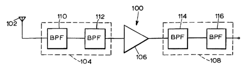
With reference now to Fig. 4, an alternative RF receiver indicated
generally at 100 includes an antenna 102, a first RF filter stage 104, an
amplifier stage 106 similar to the amplifier stage 16, and a second RF filter
stage 108. In one embodiment, the first RF filter stage 104 includes a pair
of cascaded RF bandpass filters 110 and 112, while the second RF filter
stage also includes a pair of cascaded RF bandpass filters 114 and 116.
CA 02349324 2001-05-O1
WO 00/08775 PCTNS99/17760
-16-
Because the pairs of bandpass filters 110, 112, 114, 116 are directly
cascaded, each RF filter is preferably a low order filter. In this manner, the
direct cascading of the filters will not result in any detrimental loading
effects.
The amplifier stage 106, however, allows the benefits of the two
filter stages 104 and 108 to be combined. More particularly, if the
individual filters I10, 112, 114, 116 are, for example, six to eight pole
filters, the RF filter stages I04 and 108 would interact detrimentally without
the intervening amplifier stage 106 serving as an isolator.
Referring now to Fig. 5, the thin film filters 110, 112, 114, 116 may
be spread over four dielectric chips 118A, 118B, 118C, 118D, respectively.
Disposing each respective filter on a corresponding separate chip will
provide more space, thereby alleviating the power density problem. Each
chip includes a dielectric substrate 120 and suitable bonding wires
schematically indicated at 122. The bonding wires 122 of the RF filters 112
and 114 are coupled to the amplifier stage 106, which may or may not be
disposed on a separate chip. Alternatively, the RF filters of the first RF
filter stage 104 may be disposed on a first substrate, while the RF filters of
the second RF filter stage 108 are disposed on a second substrate.
The foregoing detailed description has been given for clearness of
understanding only, and no unnecessary limitations should be understood
therefrom, as modifications would be obvious to those skilled in the art.