Note: Descriptions are shown in the official language in which they were submitted.
CA 02349344 2001-05-O1
PCT/US99/25801
WO 00/27059
Reducing Waiting Time Jitter
The present invention relates generally to the field of telecommunications
and, in particular, to reducing waiting time fitter in systems in which pulse
stuffing
is used to synchronize an asynchronous signal for transmission over a
synchronous
communication link.
When a connection is made through a telecommunications network, some
10 portions of the connection may be asynchronous to the local clock of
another
portion or link of the connection. "Bit stuffing" techniques have been used to
synchronize digital signals from an asynchronous link with a local clock of a
synchronous link. These bit stuffing techniques selectively add bits to and/or
subtract bits from frames of data to adjust the length of the frames for
15 transmission over the synchronous link. Once synchronized, the digital
signal
can be conveniently switched or transmitted with other, similarly
synchronized,
digital signals.
One bit stuffing technique is positive stuffing, in which it is assured that
the frequency of the synchronized data signal is equal to or greater than the
20 highest possible frequency of the asynchronous data signal, and frequency
differences are made up by the insertion of stuff bits. For example, an
asynchronous DS1 data signal has a frequency of 1.544Mb/s ~75b/s, and may be
converted by positive stuffing into a synchronized data signal with a
frequency
of at least 1.544075Mb/s. Generally, a higher frequency than this is used for
the
25 synchronized data signal in order to enable waiting time fitter, which
arises as a
result of the stuffing process and has a frequency component equal to the
stuffing
frequency, to be subsequently filtered out from the synchronized data signal.
Even though this technique of positive stuffing has been effective for
some time, it cannot be readily used in a so-called synchronous transmission
30 network in which incoming asynchronous and synchronous data signals must be
accommodated to produce an outgoing synchronized data signal having
CA 02349344 2001-05-O1
WO 00/27059 PCT/US99/25801
substantially the same frequency as the incoming synchronous data signals.
Synchronous networks are becoming of increasing importance in the
communication of data signals.
In a synchronous network, an incoming synchronous data signal is
S already synchronized to the correct frequency so that there is no need to
provide
a synchronizing arrangement for such a signal. An incoming asynchronous data
signal, however, can have a frequency which is either lower or higher than the
synchronized data signal frequency, and a synchronizing arrangement is
required
in order to effect positive or negative stuffing, respectively, to produce a
synchronized data signal from the asynchronous data signal. Whereas positive
stuffing comprises providing a stuff bit in the synchronized data signal to
compensate for a relatively lower asynchronous data signal frequency, negative
stuffing comprises using a 'spare' bit of the synchronized data signal for
transmitting data to compensate for a relatively higher asynchronous data
signal
frequency.
With this positive/negative stuffing, the synchronized data signal has a
waiting time fitter component at a frequency which is equal to the rate of
positive
or negative stuffing. The closer the asynchronous data signal frequency is to
the
synchronized data signal frequency, the lower will be the stuffing rate and
hence
the fitter component frequency, rendering it more difficult to filter out the
fitter
from the synchronized data signal. Using a phase-locked loop (PLL) to filter
out
fitter, the need to handle lower frequency fitter components results in the
disadvantages of increased acquisition times, memory requirements, and
latency.
In a bit stuffing synchronizing arrangement, this fitter component,
referred to generally as "waiting time fitter," has a frequency which is equal
to
the nominal rate of positive or negative stuffing. For example, if the
tributary
data is an asynchronous DS1 bit stream having a nominal bit rate of 1.544 Mb/s
and an actual bit rate which may be up to 75b/s more or less than this, then
the
fitter component will have a frequency in the range from 0 to 75Hz. The closer
the asynchronous bit stream rate is to the nominal rate, the lower the
frequency
of the fitter component.
In a receiver to which the bit stream is ultimately transmitted, a
dejittering phase locked loop (PLL) is provided to reduce fitter, but this
generally
2
CA 02349344 2001-05-O1
WO 00/27059 PCT/US99/25801
has a lower cut-off frequency of at least about 3 Hz so that most fitter due
to
stuffing is not attenuated by this PLL. This gives rise to a significant
problem in
the handling of asynchronous digital bit streams in some synchronous networks.
The cut-off frequency of the receiver PLL cannot be substantially reduced to
avoid the problem because this would unacceptably increase the acquisition of
the PLL and elastic storage requirements, and in any event this cut-off
frequency
would have to be reduced to 0 to handle all possible f fitter frequency
components.
For the reasons stated above, and for other reasons stated below which
will become apparent to those skilled in the art upon reading and
understanding
the present specification, there is a need in the art for circuits and methods
for
reducing waiting time fitter in telecommunications networks.
The above mentioned problems with telecommunications networks and
other problems are addressed by the present invention and will be understood
by
reading and studying the following specification. Circuits and methods are
described which reduce waiting time fitter by using, at a
synchronizer/multiplexer, a "sub-bit" comparison of a clock associated with an
unsynchronized data stream and a clock associated with a synchronized data
stream to generate a threshold level for use in determining when to stuff bits
into
the synchronized data stream. The term "sub-bit" means that the phase
difference, as measured by, for example, the location of pointers associated
with
the two clocks, is precise to a fraction of a bit or has a "fractional
component."
This sub-bit comparison essentially measures the waiting time fitter and is
used
to adjust the threshold level so as to reduce at least the low frequency
components of the waiting time fitter at the synchronizer/multiplexer before
transmission to the desynchronizer/demultiplexer.
Figure 1 is a block diagram of an embodiment of a communications
system according to the teachings of the present invention.
Figure 2 is a schematic representation of an embodiment of a data packet.
Figure 3 is a block diagram of one embodiment of a
synchronizer/multiplexer circuit for use in the system of Figure 1.
3
CA 02349344 2001-05-O1
WO 00/27059 PCT/US99/25801
Figure 4 is a graph that illustrates an embodiment of a decision criteria
for a limiter circuit of Figure 3.
Figure 5 is a flow chart that illustrates an embodiment of a process for
controlling the insertion of stuff pulses in a synchronizer/mulitplexer
circuit.
Figure 6 is a graph that illustrates representative signals for the operation
of the synchronizer/mulitplexer of Figure 3.
Figure 7 is a black diagram of an another embodiment of a
synchronizer/mulitplexer according to the teachings of the present invention
The following detailed description refers to the accompanying drawings
which form a part of the specification. The drawings show, and the detailed
description describes, by way of illustration specific illustrative
embodiments in
which the invention may be practiced. These embodiments are described in
sufficient detail to enable those skilled in the art to practice the
invention. Other
embodiments may be used and logical, mechanical and electrical changes may
be made without departing from the scope of the present invention. The
following detailed description is, therefore, not to be taken in a limiting
sense.
Figure 1 is a block diagram of an embodiment of a communications
system, indicated generally at 100, according to the teachings of the present
invention. System 100 includes multiplexes (MUX) 102 and demultiplexer
(DEMUX) 104 that are coupled by synchronous link 106. Link 106 comprises,
for example, an high-bi-rate digital subscriber line ("HDSL") link over a
medium such as microwave, wired or other appropriate medium. Link 106 may
comprise any other appropriate synchronous transmission medium or link.
Multiplexes 102 receives data in an unsynchronized format, e.g., DS1
data. The unsynchronized data can be other conventional or later developed
asynchronous data formats that are coupled to and transmitted over a portion
of a
synchronous link or transmission medium. System 100 uses stuff bits at
multiplexes 102 to synchronize the unsynchronized data with the clock of link
106. As shown in Figure 2, multiplexes 102 creates frames from the received,
unsynchronized data. The frames include a number of fields. These fields
include synchronization (sync) bits, payload data, overhead data and a number
of
stuff bits. As described above, this number of stuff bits can vary from frame
to
4
CA 02349344 2001-05-O1
WO 00/27059 PCT/US99/25801
frame. In the embodiment shown in Figure 2, the nominal case is to include two
stuff bits. Multiplexes 102 can depart from this nominal case by including
more
or fewer bits in the frame to create an acceptable stream of data that is
synchronized for transmission over link 106.
S At demultiplexer 104, the synchronized data is desynchronized.
As described above, when clocks associated with the synchronized and
unsynchronized data streams are close in frequency, low frequency waiting time
fitter may be introduced by the bit stuffing process. Advantageously, -
multiplexer 102 uses an adjustable threshold level to determine when to
compensate for a difference in these clocks by stuffing bits into the
synchronized
data stream. This threshold level is determined based on a sub-bit comparison
of
a clock associated with the unsynchronized data stream and a clock associated
with the synchronized data stream. This "sub-bit" comparison essentially
measures the approximate waiting time fitter introduced into the synchronized
data stream. Based on the sub-bit comparison, the threshold level used to
determine when to insert stuff bits into the synchronized data stream is
varied
among, for example, two or three levels so as to compensate for, or reduce,
the
waiting time fitter at multiplexes 102.
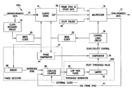
Figure 3 is a block diagram of an embodiment of a
synchronizer/multiplexer circuit, referred to generally as "multiplexes 102a,"
for
use in system 100 of Figure 1. Multiplexes 102a receives an unsynchronized
data stream at input 10 and produces a synchronized data stream at output 12.
Multiplexes 102a includes elastic store 14 that acts as a buffer to store the
unsynchronized data that arrives at input 10. Clock recovery circuit 18 and
write
clock 20 are coupled to provide a clock signal to control the storage of the
unsynchronized data in elastic store 14.
Read clock 22 controls the reading of data out of elastic store 14 to create
the synchronized data stream at output 12.
Write clock 20 and read clock 22 are both coupled to phase comparator
24 to control when stuff pulses or bits are inserted into the synchronized
data
stream at output 12. Phase comparator 24 provides an input to comparator 34.
Comparator 34 provides a stuff/delete control signal to control logic 36.
Control
logic 36 further provides an input to read clock 22 and a control signal to
5
CA 02349344 2001-05-O1
WO 00/27059 PCT/US99/25801
multiplexes 16. This control signal indicates to multiplexes 16 when to insert
pulses or "stuff bits" (indicated at block 40) into the synchronized data
stream at
output I2. For example, if read clock 22 is slightly slower than write clock
20,
control logic 36 instructs multiplexes 16 to, in effect, delete stuff pulses
from
selected frames in the synchronized data stream at output 12. This allows the
read clock 22 to catch up with the write clock 20. Alternatively, if read
clock 22
is too fast, control logic 36 instructs multiplexes I6 to add more stuff
pulses to,
in effect, slow down read clock 22. Thus, phase comparator 24, comparator 34, -
-
and control logic 36 work to create a synchronized data stream at output 12
from
the unsynchronized data stream at input 10.
Multiplexes 16 is coupled to receive three inputs that can be included in
the synchronized data stream at output 12. First, the output of elastic store
14
provides the data from unsynchronized data at input 10. Additionally, frame
sync and other data are provided at block 38. As mentioned above, stuff pulses
are also provided at block 40. The control signal from control logic circuit
36
controls the generation of the stream of data at output 12 by multiplexes 16
using
data from elastic store 14, block 38 and block 40.
Multiplexes 102a also includes a control circuit that is used to reduce the
introduction or effect of low frequency waiting time fitter on the
synchronized
data stream at output 12. In this embodiment, this control circuit includes
phase
detector 31 and threshold generator 33. Phase detector 31 essentially provides
a
measure of the waiting time fitter in the synchronized data stream at output
I2.
Threshold generator 33 modifies the threshold value used by comparator 34 to
make stuff decisions so as to compensate for or reduce the effect of low
frequency waiting time fitter in the synchronized data stream at output 12.
Phase detector 3.1 compares two clock signals and produces an output
signal. Phase detector 31 includes divider 26 that is coupled to receive a
first
clock signal from write clock 20. Divider 26 divides this clock signal down to
produce a reference sync signal. The divide-by-value is chosen such that the
nominal reference sync signal out of divider 26 is substantially the same
frequency as the nominal frame rate. For instance, when transmitting DS 1 over
HDSL2, there are 9264 DS 1 data bits in one HDSL2 frame. Therefore, the
divider 26 for HDSL2 transmission would have a divide-by-value of 9264. The
6
CA 02349344 2001-05-O1
WO 00/27059 PCT/US99/25801
divide-by-value of divider 26 can be varied when other data formats are used
for
the synchronized and unsynchronized data.
The second clock signal is frame sync 41 taken from multiplexes 16.
This frame sync is, in one embodiment, a DSL frame synchronization clock
signal. Frame sync 41 and the reference sync signal from divider 26 are
provided to lead/lag counter 28 to produce a signal to threshold generator 33.
Lead/lag counter 28 is controlled by an external clock with a frequency that
is
sufficient to create an error signal with sub-bit or fractional precision.
This error -
signal is provided to threshold generator 33.
Threshold generator 33 includes low pass filter 30 and limiter 32. Low
pass filter 30 filters the error signal from phase detector 31 to produce a
signal
that represents the low frequency waiting time fitter in the synchronized data
stream at output 12. The bandwidth of low pass filter 30 is on the order of 3
Hz
or less. Limiter 32 is coupled to low pass filter 30 and creates a threshold
level
1 S based on the output of low pass filter 30. For example, Figure 4 provides
a
graph that represents the function of limner 32. In the graph of Figure 4, the
output of low pass filter 30 is plotted along the X axis and the output of
limiter
32 is plotted along the Y axis. In this example, limner 32 can produce one of
three stuff threshold values based on the detected low frequency waiting time
fitter; namely, K unit intervals (UI), 0 UI, or -K UL The magnitude of the
value
K depends on the application but is a constant for a given combination of
nominal data clock and frame structure. The value of K must be large enough to
effect a change in the existing stuff/delete pattern and reduce waiting time
fitter.
For minimum waiting time fitter, the smallest effective value of K should be
used. For instance, HDSL and HDSL2 are both used to transmit DS 1 data
although their frame structures are different. The appropriate value of K is 2
for
HDSL and 1 for HDSL2.
If the output of filter 30 is above a selected value, nsbound, then limiter
32 outputs a stuff threshold of -K UI. If the output of filter 30 is below a
second
selected value, -nsbound, then limiter 32 outputs a stuff threshold of +K UI.
Finally, if the output of filter 30 is between the two selected levels, then
limiter
32 outputs a nominal stuff threshold of 0 UI. The variation of the stuff
threshold
level allows comparator 34 to selectively insert stuff bits so as to reduce
the
7
CA 02349344 2001-05-O1
WO 00/27059 PCT/US99/25801
effect of waiting time fitter at the generation of the synchronized data
stream at
output I2.
In another embodiment, the values for nsbound and -nsbound can be set
equal to each other such that limiter 32 only produces one of two possible
output
levels. Further, it is noted that other output levels for limiter 32 can be
chosen
for a specific implementation.
Figure S is a flow chart of an embodiment of a process for comparator 34.
Comparator 34 makes a decision at block 17 as to whether the measured phase
from phase comparator 24 exceeds the threshold level indicated by threshold
generator 33. If not, then a short frame is sent. If, however, the phase
difference
does exceed the threshold, then a stuff decision is made and a long frame is
sent.
Figure 6 is a graph that represents the operation of multiplexes 102a on a
test unsynchronized data stream at input 10. This graph includes three traces;
namely filter trace 23, threshold trace 25 and stuff trace 27. The values for
nsbound and -nsbound in this example were set at +20 nanoseconds (ns) and -20
ns, respectively. Further, limiter 32 produced a stuff threshold value with
one of
three possible levels; namely, -1, 0 and +1.
Filter trace 23 is the output of filter 30. This trace represents,
effectively,
the low frequency waiting time fitter of the synchronized data stream at
output
12. When the level of filter trace 23 stays between the +20 ns, stuff
threshold
trace 25 stays at 0 UI as identified, for example, at 61 and 63. When the
level of
filter trace 23 travels below -20 ns, the threshold level is increased to 1 UI
as
shown, for example, by threshold trace 25 at 65. When filter trace 23 exceeds
+20 ns, the threshold is decreased to -1 UI to compensate as shown, for
example,
at 67. This modification of the threshold level based on the level of the
output of
filter 30 reduces the tendency of the error signal from phase detector 31 to
move
in one direction or the other, and consequently, the waiting time fitter is
reduced.
Figure 7 is a block diagram of an alternative embodiment of a
synchronizer/multiplexer, indicated generally at 102b, according to the
teachings
of the present invention. Multiplexes 102b varies from multiplexes 102a in the
manner in which the sub-bit phase detection is accomplished. Therefore, for
simplicity, the similar aspects of multiplexes 102a will not be repeated here.
8
CA 02349344 2001-05-O1
WO 00/27059 PCT/US99/25801
Multiplexer 102b includes sub-bit phase detector 24' which compares the
phase difference of write and read clocks 20 and 22, in a manner that provides
a
signal that includes both a bit level and a sub-bit or fractional comparison
of the
relative phases of the clocks. The bit level component of the comparison is
provided to comparator 34 to be used in determining when to insert stuff bits
into the synchronized data stream at output 12. The sub-bit level comparison
is
used by threshold generator 33' to set the threshold level for comparator 34.
Threshold generator 33' operates in a similar manner as threshold generator 33
of
Figure 1.
In this embodiment, the comparison of write clock 20 and read clock 22
on a sub-bit or fractional level provides an approximate measurement of the
waiting time fitter in a manner similar to lead/lag counter 28 of Figure 1.
Although specific embodiments have been illustrated and described
herein, it will be appreciated by those of ordinary skill in the art that any
arrangement which is calculated to achieve the same purpose may be substituted
for the specific embodiment shown. This application is intended to cover any
adaptations or variations of the present invention. For example, the output of
limiter 32 could be provided to an adder in the path between phase detector 24
or
24' and comparator 34 to effectively modify the threshold of comparator 34 by
modifying the error signal provided to the comparator. Further, the values
used
as the threshold can be modified as necessary for a specific application.
Threshold levels other than -1, 0 and +1 UI could be used. Further, other
clocks
that can give a measure of the waiting time fitter at the multiplexer can be
used
as a basis for generating a threshold level for comparator 34.
9