Note: Descriptions are shown in the official language in which they were submitted.
CA 02349478 2003-08-22
Direct Digital Frequency Synthesizer And A Hybrid
Frequency Synthesizer Combining A Direct Digital
Frequency Synthesizer And A Phase Locked Loop
BACKGROUND
1. Field of the Invention
This application relates generally to frequency synthesizers. More
specifically, the application describes a novel direct digital frequency
synthesizer
(DDFS), and a hybrid frequency synthesizer combining a novel DDFS and a phase
locked loop (PLL).
l0 2. Description of the Related Art
The frequency synthesizer is an important element of a wireless device. It
controls the frequency of transmission and reception, and should, therefore,
generate an output signal with an accurate frequency which has low spurious
CA 02349478 2001-06-O1
levels, low phase noise, and good frequency resolution. In addition, the
compact
nature of modern mobile devices creates a need for frequency synthesizers
which
have low power consumption, require few external components, and occupy very
little space.
In many mobile devices, frequency synthesizers are also used to modulate
the transmission signal. With a rising demand for systems capable of complex
modulation schemes such as Quadrature Amplitude Modulation (QAM) or
Quaternary Phase Shift Keying (QPSK), there is a need for frequency
synthesizers
which have very high switching speeds and which are capable of performing
to complex modulations and compressing high data rates into a narrow RF
spectrum.
Two circuits commonly used for frequency synthesis are the phase locked
loop frequency synthesizer (PLL) and the direct digital frequency synthesizer
(DDFS). FIG. 1 sets forth a block diagram of a known phase locked loop
frequency synthesizer. In this Circuit, the free running frequency of the
voltage
controlled oscillator (VCO) 18. is divided by a factor of N in a divider 20,
and
compared with a reference input frequency (Fref) by a phase detector 12. The
phase detector 12 generates an error signal which controls the direction of a
current pulse generated by a charge pump 14 based on the phase difference
between Fref and the feedback signal. A loop filter l 6 then converts the
current
pulse from the charge pump 14 into a DC voltage which controls the frequency
of
the VCO output. When the loop is locked, Fout is equal to N*Fref.
2
CA 02349478 2001-06-O1
Although the PLL shown in FIG. 1 is useful for generating high
frequencies locked to a reference frequency, its use in high performance
mobile
devices is limited because of its slow switching speed, relatively large step
size
(equal to Fref) and spurious output. In addition, because the PLL has a fixed
input (Fref), its output signal .frequency can only be changed by changing the
division ratio N. This feature limits the utility of such PLLs in mobile
systems
having complex modulation schemes.
FIG. 2 shows a blocl{ diagram of a known direct digital frequency
synthesizer (DDFS). In this circuit, a reference frequency (Fref) is used by a
to phase accumulator 24 to generate a discrete phase signal having phase
increments
controlled by a frequency control word (FCW) input to the phase accumulator
24.
Since the phase accumulator 2;4 has fixed output word length, the accumulated
phase value will eventually overflow, such that the discrete phase signal is a
substantially periodic signal having a period T as shown in FIG. 2. The
discrete
phase signal is then used to adldress a sine lookup ROM 26, which generates a
discrete waveform having a frequency equal to the inverse of the discrete
phase
signal period (1/T). The discrete waveform is converted to a continuous
waveform by a digital to analog converter (:DAC) 28, and is smoothed by a
deglitcher 30 and low pass filter 32.
2o This known DDFS 22 lzas a high switching speed and can be used for
accurate modulation. Its utility in high performance systems is limited,
however,
3
CA 02349478 2001-06-O1
due to its spurious output and large power consumption at high frequencies.
The
spurious output associated with I~DFS 22 is caused by the non-linear nature of
the
DAC 28, and the finite word length effects in the sine lookup :ROM 26 and DAC
28. The location and level of these spurious signals have been analyzed in "An
analysis of the output Spectrum of Direct Digital Frequency Synthesizers in
the
presence of Phase Accumulatol° Truncation," Henry T. Nicholas, and
Henry
Samueli, 41~' Annual Freauency Control Symposium, 1987, "The Optimization of
Direct Digital Frequency Synthesizer Performance in the presence of Finite
Word
Length Effects," Henry T. Nicholas, Henry Samueli, and Bruce Kin,
42°
to Freauency Control Symposium, 1988, pp 357-363, and "An Exact Spectral
Analysis of a Number Controlled Oscillator Based Synthesizer," Joseph F.
Garvey, Daniel Babitch, 44~' Annual Freauency Control Symnosium, 1990, pp
511-521. It has been shown that the dominant component of the spurious content
is due to the phase errors introduced by phase truncation at the output of the
phase
accumulator 24.
In addition, the maximum frequency that can be directly generated from
the DDFS 22 shown in FIG. 2 is equal to one half the reference frequency
(Fref/2). Practically, only 30% of :Fref can be generated. Consequently, in a
system requiring frequencies on t;he order of tens or hundreds of MHz, the
2o reference frequency must be very Thigh. The power consumption necessary to
4
CA 02349478 2001-06-O1
generate the required reference frequency makes it difficult to integrate this
known DDFS 22 into most next generation mobile devices.
FIG. 3 shows a block diagram of a known hybrid frequency synthesizer
34. This hybrid circuit 34 combines the DDFS 22 shown in FIG. 2 with the PLL
10 shown in FIG. 1. The PLL ll U in this circuit uses the lower frequency
output of
the DDFS 22 as its reference frequency, and converts it into a higher
frequency
output signal suitable for use in mobile devices. This hybrid combination 34
resolves some of the problems associated with the synthesizers shown in FIG. 1
and FIG. 2. Nonetheless, this known hybrid 34 is unsuitable for many high
to performance mobile applications because of its large power consumption and
spurious output. In order to increase the output of the DDFS 22 to a frequency
in
the RF range, the PLL 10 must have a large division ratio N. The cost of a
large
division ratio N is that the spurious signals generated by the DDFS 22 are
exponentially increased in strength by the PLL 10 and passed through to the
~'.5 frequency synthesizer output. 1V(oreover, the DDFS 22 cannot generate an
output
with acceptably low spurious signals without utilizing a very high reference
frequency on the order of hundreds of MHz. This requires an unacceptable trade-
off between power consumption and signal integrity.
Briefly stated, the relatively high power consumption and output noise
2o associated with known frequency synthesis techniques limit their
application in
power and noise sensitive environments, such as mobile communications systems.
5
CA 02349478 2003-08-22
Moreover, most current research in frequency synthesizer design is focused on
obtaining
higher frequencies, close to 1 GHz, directly from a DDFS. Unfortunately,
circuits of this type
require clock frequencies of 2 GHz and higher, and, therefore, exhibit power
consumption on
the order of Watts. This direct synthesis approach is not feasible in portable
wireless
applications where battery life and power consumption are critical parameters.
SUMMARY
A direct digital frequency synthesizer and a hybrid frequency synthesizer
combining
the direct digital frequency synthesizer and a phase locked loop is -provided.
The direct
digital frequency synthesizer includes a phase accumulator -that is configured
to generate a
1o discrete phase signal. Spurious phase modulation .in the discrete phase
signal is reduced by a
noise shaper, and the output of the noise shaper is then used to address a
phase-to-amplitude
translator. The phase-to-amplitude translator generates a discrete waveform
which is
converted to a continuous waveform by a digital to analog converter. The
hybrid frequency-
synthesizer uses a mixer to combine a reference frequency generated by a
reference source
and a DDFS output signal generated by a direct digital frequency synthesizer.
The output
from the mixer is then coupled to the input of a phase locked loop which
multiplies the mixer
output to generate the frequency synthesizer output.
In accordance with an aspect of the present invention, there is provided a
hybrid
frequency synthesizer, comprising a reference source configured to generate a
reference
2o frequency signal; direct digital frequency synthesizer (DDFS) configured to
generate a DDFS
output signal; a mixer coupled to the DDFS and the reference source, and
configured to
combine the reference frequency signal and the DDFS output signal to generate
a mixer
output signal; and a phase locked loop frequency synthesizer (PLL) coupled to
the mixer, and
6
CA 02349478 2003-08-22
configured to generate a frequency synthesizer output that is a multiple of
the mixer output
signal; wherein the DDFS comprises a phase accumulator configured to generate
a discrete
phase signal; a sine lookup ROM addressed by the discrete phase signal that
generates a
discrete waveform; a digital to analog converter (DAC) coupled to the sine
lookup ROM that
converts the discrete waveform into a continuous waveform of substantially
equal frequency;
a low pass filter coupled to the DAC that smoothes the continuous waveform;
and a
deglitcher coupled between the DAC and the low pass filter that reduces
spurious signals
generated by the DAC.
In accordance with another aspect of the present invention, there is provided
a hybrid
frequency synthesizer, comprising a reference source configured to generate a
reference
frequency signal; a direct digital frequency synthesizer (DDFS) configured to
generate a
DDFS output signal; a mixer coupled to the DDFS and the reference source, and
configured
to combine the reference frequency signal and the DDFS output signal to
generate a mixer
output signal; and a phase locked loop frequency synthesizer (PLL) coupled to
the mixer, and
configured to generate a frequency synthesizer output that is a multiple of
the mixer output
signal; wherein the DDFS comprises a phase accumulator configured to generate
a discrete
phase signal; a noise shaper that reduces spurious phase modulation in the
discrete phase
signal, and which generates a discrete noise shaper output; and a phase-to-
amplitude
translator addressed by the discrete noise shaper output for generating a
discrete waveform
that comprises the DDFS output signal, wherein the phase-to-amplitude
translator comprises
a ones complementor coupled to the discrete noise shaper output, and
configured to
sequentially generate a pass-through output and an inverted output; a read
only memory
(ROM) coupled to the ones complementor and configured to generate a first
quadrant of the
discrete waveform when addressed by the pass-through output and a second
quadrant of the
6a
CA 02349478 2003-08-22
discrete waveform when addressed by the inverted output; and means for
inverting the first
and second quadrants of the discrete waveform to generate a third and fourth
quadrant of the
discrete waveform.
In accordance with yet another aspect of the present invention, there is
provided a
hybrid frequency synthesizer, comprising a reference source configured to
generate a
reference frequency signal; a phase accumulator configured to generate a
discrete phase
signal; a noise shaper that reduces spurious phase modulation in the discrete
phase signal,
and which generates a discrete noise shaper output; a phase-to-amplitude
translator addressed
by the discrete noise shaper output that generates a discrete sine waveform
and a discrete
~o cosine waveform; a digital image reject mixer coupled to the phase-to-
amplitude translator
and the reference source, and configured to combine the reference frequency
signal and the
discrete sine and cosine waveforms to generate a mixer output signal having a
most
significant bit (MSB); and a phase locked loop frequency synthesizer (PLL)
having an input
which is coupled to the MSB of the mixer output signal, and which is
configured to generate
a frequency synthesizer output that is a multiple of the mixer output signal.
In accordance with yet another aspect of the present invention, there is
provided a
hybrid frequency synthesizer, comprising a reference source configured to
generate a
reference frequency signal; a phase accumulator configured to generate a
discrete phase
signal; a noise shaper that reduces spurious phase modulation in the discrete
phase signal and
2o which generates a discrete noise shaper output; a phase-to-amplitude
translator addressed by
the discrete noise shaper output that generates a discrete sine waveform and a
discrete cosine
waveform; a digital image reject mixer coupled to phase-to-amplitude
translator and the
reference source, and configured to combine the reference frequency signal and
the discrete
sine and cosine waveforms to generate a mixer output signal; a band pass sigma
delta
6b
CA 02349478 2003-08-22
modulator coupled to the image reject mixer that converts the mixer output
signal into a
modulated one bit signal; and a phase locked loop frequency synthesizer (PLL)
having an
input coupled to the modulated one bit signal, and configured to generate a
frequency
synthesizer output that is a multiple of the modulated one bit signal.
In accordance with a further aspect of the present invention, there is
provided a direct
digital frequency synthesizer, comprising a phase accumulator configured to
generate a
discrete phase signal; a noise shaper that reduces spurious phase modulation
in the discrete
phase signal, and which generates a discrete noise shaper output; a phase-to-
amplitude
translator addressed by the discrete noise shaper output that generates a
discrete waveform; a
1o digital to analog converter (DAC) coupled to the phase-to-amplitude
translator that converts
the discrete waveform to a continuous waveform; and a reference source coupled
to a clock
input of the phase accumulator.
6c
CA 02349478 2001-06-O1
BRIEF DESC;RIPTION OF THE DRAWINGS
FIG. 1 is a block diagram of a known phase locked loop frequency
synthesizer;
FIG. 2 is a block diagram of a known direct digital frequency synthesizer;
FIG. 3 is a block diagram of a known hybrid frequency synthesizer;
FIG. 4 is a block diagram of an exemplary hybrid frequency synthesizer
according to the present invention;
FIG. 5 is a block diagram of an exemplary embodiment of a hybrid
to frequency synthesizer including an improved direct digital frequency
synthesizer
and a digital image reject mixer according to the present invention;
FIG. 6 sets forth block diagrams of an exemplary first order noise shaper
and an exemplary second order noise shaper;
FIG. 7 is a block diagrann of an exemplary digital image reject mixer;
FIG. 8 is a block diagram of an exemplary half band filter;
FIG. 9 is a block diagram of an exemplary fifth order sigma delta
modulator;
FIG. 10 :is a block diagram showing a more detailed representation of the
integrator blocks shown in FIG. 9;
7
CA 02349478 2001-06-O1
FIG. 11 is a block diagram of an exemplary integrator for transforming the
fifth order sigma delta modulator shown in FIG. 9 into a band pass sigma delta
modulator;
FIG. 12 is a block diagram of an exemplary direct digital frequency
synthesizer implementing 25x 16 bit ROMs for use with hybrid frequency
synthesizers as shown in FIG. 5; and
FIG. 13 is a block diagram of an exemplary direct digital frequency
synthesizer.
1o DET~~.ED DESCRIPTION
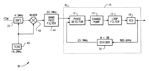
Turning now to the drawing figures, FIG. 4 is a block diagram of an
exemplary hybrid frequency synthesizer 38 according to the present invention.
This circuit 38 includes a direct digital frequency synthesizer (DDFS) 22, a
temperature controlled crystal oscillator (TCXO) 40, a mixer 42, a band pass
filter
44, and a phase locked loop frequency synthesizer (PLL) 10. The PLL 10
includes a phase detector 12, a charge pump 14, a loop filter 16, a voltage
controlled oscillator (VCO) 18, and a divider 20. Operationally, this circuit
uses
the mixer 42 to aum the output frequencies of the DDFS 22 and TCXO 40, and
uses the higher frequency mixer output signal as the input to the PLL 10. It
should be understood that the specific numerical values shown are given as an
example only.
8
CA 02349478 2001-06-O1
The DI)FS 22 receives a clock input (also called a reference frequency
signal) from the TCXO 40 amd a frequency control word input (FCW), and
generates a DDFS output signal. The DDFS 22 may be any known DDFS,
including the known DDFS 2:Z shown in FIG. 2. The frequency of~the DDFS
output signal (4.5 MHz) is increased by the mixer 42, which combines it with
the
reference frequency signal ( 19.2 MHz) to generate a mixer output signal (23
.7
MHz). The mixer output signal is smoothed by the band pass filter 44 and
coupled to the PLL 1U. The PL L 10 then multiplies the signal by a division
ratio
N and locks it in phase.
The PLL 10 can be any known phase locked loop synthesizer having the
necessary division ratio N, including the PLL 10 shown in FIG. 1. In this
exemplary embodiment, the PLL 10 includes the voltage controlled oscillator
(VCO) 18, which generates the frequency synthesizer output. The frequency
synthesizer output is divided by a factor of N in divider 20, and fed back to
the
phase detector 1.2. The phase detector 12 compares this feedback signal with
the
smoothed mixer output signal fi-om the band pass filter 44, and generates an
error
signal. The error signal then controls the direction of a current pulse
generated by
the charge pump 14 based on the phase difference between the feedback signal
and the smoothed mixer output signal. The loop filter 16 converts the current
2o pulse from the charge pump 14 into a DC voltage which controls the
frequency of
the VCO 18.
9
CA 02349478 2001-06-O1
The use of the mixer 42 in this exemplary embodiment 38 to boost the
frequency of the DDFS output signal, makes it possible to utilize a PLL 10
having
a reduced division ratio N. Depending on the data network (e.g., Mobitex,
Datatac, CDPD), division ratios can be in the range of about 32 to about 39.
The
reduction in the value of N to 38 in this embodiment makes it possible to
utilize a
hybrid frequency synthesizer structure to generate frequencies in the RF range
without generating high dB level spurious signals in the frequency synthesizer
output which are incompatible 'with mobile applications.
FIG. 5 is a block diagram of an exemplary embodiment of a hybrid
to frequency synthesizer including an improved direct digital frequency
synthesizer
and a digital image reject mixer according to the present invention. The
circuit
46 shown in FIG. 5 includes a ;>erial port 48, a TCXO 40, an improved DDFS 67,
a digital image reject mixer 58, a divide by four divider 60, a band pass
sigma
delta modulator 62, an analog filter 64, and a PLL 10. The improved DDFS 67
includes a phase accumulator 24, a noise shaper 50, a phase-to-amplitude
translator 52, and a first and second half band filter 56a and 56b. The PLL 10
includes a phase detector 12, a charge pump 14, a loop filter 16, a VCO 18,
and a
divider 20. It should be understood, however, that the specific numerical
values
shown are given as examples only.
2o The output frequency of this circuit 46 is tuned using a frequency control
word input (FCW), which is coupled to the accumulator 24 of the DDFS through
CA 02349478 2001-06-O1
a serial port 48. The accumulator receives the FCW and a reference frequency
signal (Fref) from the TCXU 40, and generates a discrete phase signal having
phase increments, and thus a period T, controlled by the FCW. The discrete
phase signal is coupled to a noise shaper 50, which reduces the spurious phase
modulation (noise) at the desired output frequency. The noise shaper 50 can be
any known noise shaper employing first order sigma delta modulation or higher.
The discrete noise shaper output is then used to address the phase-to-
amplitude
translator (ROlV~ 52, which generates a discrete sine waveform 54a and a
discrete
cosine waveforrn 54b, each having a frequency substantially equal to the
inverse
of the period of the discrete phase signal ~ 1 ~ .
T
The discrete sine and cosine waveforms 54a and 54b generated by the
phase-to-amplitude translator 52: are filtered by half band filters 56a and
56b, and
are coupled to the digital image reject mixer 58. Each of the half band
filters 56a
and 56b can be any known half~band filter capable of reducing noise at F'ef
2 '
which is effectively folded b<ick over the desired discrete sine and cosine
waveforms 54a and 54b as a result of the multiplication function performed by
the
digital image reject mixer 58.
The divide by four divider 60 divides the reference frequency signal (FrefJ
in order to generate a 0° phased clock pulse and a 90° phased
clock pulse, each
11
CA 02349478 2001-06-O1
having a frequf.ncy substantialliy equal to F4ej . The digital image reject
mixer 58
receives the discrete sine and cosine waveforms 54a and 54b and the 0°
and 90°
phased clock pulses, and generates a mixer output signal having a-frequency
substantially equal to F'ef +-I
4 'T
In one embodiment, the most significant bit from the mixer output is
coupled to the PLL 10 (not shown in drawings). The PLL then multiplies the
frequency of the mixer output by the division ratio N and locks it in phase as
described abovE: with respect to FIG. 4. If greater precision is desired,
however,
the entire range of the mixer output may be utilized by coupling a band pass
1o sigma delta modulator 62 betwf;en the image reject mixer 58 and the PLL 10.
The
band pass sigma delta modulator 62 converts the sixteen (16) bit mixer output
into
a modulated one bit signal where the average pulse rate at any time is equal
to the
amplitude of the; desired sine w;aveform. An analog filter 64 may also be
coupled
between the band pass sigma delta modulator 62 and the PLL 10 in order to
remove unwanted spurious signals.
The exemplary embodiment of a hybrid frequency synthesizer shown in
FIG. 5 provides a number of improvements over known hybrid frequency
synthesizers. Significantly, this embodiment can generate an RF output with
very
high spectral purity while consuming a relatively small amount of power. These
12
CA 02349478 2001-06-O1
features make this embodiment especially useful in high performance mobile
devices.
FIG. 6 sets forth block diagrams for exemplary first and second order
noise shapers 68 and 70, either of which can be used for the noise shaper 50
in
FIG. 5. The first order noise shaper 68 includes an adder 72 and a delay 74.
The
second order noise shaper 70 includes a first adder 76, a second adder 78, a
first
delay 80, a second delay 84, and a bit shift 82. Operationally, these noise
shapers
reduce spurious phase modulation close to the carrier by using known sigma
delta
techniques as described in "A Direct Digital Synthesizer with Improved
Spectral
to Performance," Paul O'Leary and Franco Maloberti, IEEE Transactions on
CommunicationsLVol. 39, No.7., July 1991, and "Delta Sigma Data Converters,
Theory, Design and Simulation," edited by Steven R. Norsworthy, Richard
Schreier, and C~abor C. Temes, IEEE Press. 1997. Simply stated, the noise
shapers 68 and 70 push noise away from the desired output frequency to higher
and lower frequencies which are; filtered out by the PLL 10.
FIG. 7 shows a block diagram of an exemplary digital image reject mixer
58. This circuit includes a first ones complementor 86, a first multiplexer
(MUX)
90, a second ones complementor 88, a second multiplexer (MUX) 92, a divide by
four divider 94, and an adder 96. The first and second ones complementors 86
2o and 88 generate at their respecti~,ve outputs the ones complements of their
inputs.
Those skilled in the art will appreciate that the complementors may be a bank
of
13
CA 02349478 2001-06-O1
inverters, for example one inverter for each input bit. The state of the
0° phased
clock pulse controls whether the multiplexer 90 selects the discrete sine
waveform
54 or its complement (generated by the first ones complementor 86). This
causes
the sine signal to be multiplied by the 0° phased clock/4 signal.
Similarly, the
s second multiplexer 92 multiplies the cosine signal with the 90°
phased clock/4
signal derived from the divide; by four divider 94. The outputs of the first
and
second multiplexers 90 and 92 are then summed in adder 96 in order to
eliminate
the image frequency.
One advantageous function of the digital image reject mixer 58 is the
1o reduction of spurious signals close to the earner. An analog mixer may
cause
inter-modulation of the DDFS output signal and the reference frequency signal.
In a digital image reject mixer 58, however, the image frequency is
eliminated,
leaving only the wanted frequency at the output of the adder 96.
FIG. 8 shows a block diagram of half band filters 56a and 56b. This
15 circuit includes six delays 98a-98f, five multipliers 100a-100e, and four
summation blocks 102a-1024, configured to filter noise at one half the
reference
frequency ~F2e~-~ . It should be understood, however, that FIG. 8 shows only
one
of numerous half band filters which may be designed for use in direct digital
frequency synthesizers such as those shown in this application, using known
14
CA 02349478 2001-06-O1
techniques as described in lVlultirate Di ital S~nal Processing, Ronald E.
Crochier and Lawrence R. Rabiner, Prentice-Hall Inc., 1983.
FIGs. 9 through I 1 show an exemplary method of constructing a band
pass sigma delta modulator 62 as set forth in "Delta Sigma Data Converters,
Theory, Design and Simulation,'" edited by Steven R. Norsworthy, Richard
Schreier and Gabor C. Temes, IEEE Press, 1997. Briefly stated, an exemplary
band pass sigma delta modulator 62 may be constructed by first designing a
less
complex low pass modulator 104 as shown in FIG. 9. Then, using the transform
z = -z z , a band pass sigma delta modulator 62 can be achieved that preserves
the
1o stability and the noise transfer fi.rnction (NTF) shape of the low pass
modulator.
FIG. 9 shows a block diagram of an exemplary fifth order sigma delta
modulator 104 (;low pass modullator), comprising five integrators 110a-110e,
and
seven multipliers, 106, 108a, 108b, and 112a-112e. FIG. 10 is a block diagram
showing a more detailed represf;ntation of the integrator blocks 110a-110e
shown
in FIG. 9. Each integrator 1 0a-110e in the low pass modulator 104 includes a
delay 120 looped back through a summation block 118. In order to transform the
low pass modulator 104 into a band pass sigma delta modulator 62, each
integrator block 1 10a-1 10e is replaced with the circuit shown in FIG. 11.
FIG. 11
includes a negative summation block 122 and two delays 124a and 124b, and
?o implements the transfer function -- 1
_ '
2 -1
CA 02349478 2001-06-O1
FIG. 12 is a block diagram of an exemplary direct digital frequency
synthesizer 126 implementing 2 5x16 bit ROMs 130a and 130b for use with hybrid
frequency synthesizers as shown in FIG. 5. This circuit includes a phase
accumulator 24, a second order noise shaper 70, a first ones complementor
128a,
a first 25x16 bit ROM 130a, a second ones complementor 128b, and a second
25x16 bit ROM 130b. Each of the ones complementors 128a and 128b operates
similarly to the ones complemf:ntor/MUX arrangements 86/90 and 88/92 in FIG.
7, to generate at its output either its input signal or the ones complement
thereof.
The phase accumulator 24, as described above with respect to FIG. 5,
to generates a discrete phase signal, having 25 bits in the embodiment shown
in FIG.
12. The second order noise shaper 70 reduces close in spurious signals and
truncates the twenty-five (25 ) bit discrete phase signal, generating a
discrete noise
shaper output having seven (7;) bits. It should be understood, however, that
this
embodiment 1:?6 is not limited to a second order noise shaper 70, but can be
1s implemented using any known noise shaper 50 employing first order sigma
delta
modulation or higher. The invention is similarly in no way limited to the
specific
numbers of bits for the signals shown in FIG. 12. The bit numbers are for
illustrative purposes only. For example, the phase accumulator 24 need not
necessarily have an output word length of 25 bits, a noise shaper may truncate
the
2o accumulator output to other than 7 bits, and the ROMs need not be
restricted to
25x16 bit ROMs
16
CA 02349478 2001-06-O1
The first ones complerr~entor 128a receives as its input the five (5) least
significant bits from the discrete noise shaper output, and is controlled by
the
second most significant bit (MSB-1). The state of MSB-1 controls whether the
first ones complementor output is equal to, or the complement of, its five (S)
bit
input.
The first 25x16 bit ROM 130a stores samples for only the first 90 degrees,
i.e. the first quadrant, of a discrete sine waveform, which is addressed by
the
output of the first ones complementor 128a. Although only first quadrant
amplitude samples are stored in the ROM 130a, a complete cycle of a sine
1o waveform may be generated, as described in further detail below.
When the first ones cornplementor output is equal to its five (5) bit input,
the ROM 130;1 generates a sixteen (16) bit output corresponding to the first
quadrant of a sinewave. When the first ones complementor output is the
complement of its five (5) bit input, the samples stored in the ROM 130a are
addressed and output in an order corresponding to the second quadrant of a
sinewave. The: most significant bit (MSB) from the noise shaper output is then
included as the sign bit of the 16 bit output from the ROM 130a. Therefore,
when
the MSB changes state, the 16 bit output of the ROM 130a becomes negative,
producing a discrete signal con-esponding to the third and fourth quadrants of
a
2o sinewave. When these operations are performed sequentially, a complete
discrete
sine wavefornu 54a is generated. Using a similar method, a discrete cosine
17
CA 02349478 2001-06-O1
waveform 54b is generated by the second ones complementor 128b, and the
second 25x16 bit ROM 130b.
In a further embodiment, both the sine and cosine waveforms may be
generated using. a single RUM, which stores either sine or cosine amplitude
samples for a single quadrant, in conjunction with appropriate addressing,
ones
complementor control and sign lbit designation arrangements. Those skilled in
the
art will appreciate that a cosine waveform is merely a 90° shifted
version of a sine
waveform. Therefore, a discrete cosine waveform may be generated from stored
sine waveform amplitude samples and vice versa.
to If a ROM, such as ROM 130a in Fig. 12 for example, stores amplitude
samples for the first quadrant of a sine waveform, then a complete sine
waveform
may be generated using a ones complementor (such as 128a), a complementor
control bit and m output sign bit as described above. A cosine waveform may
also be generated from the same: ROM using a similar addressing, control bit
and
sign bit arrangement, but with the addition of an address offset component,
such
as an adder, to provide for the '90° phase shift. The address offset is
preferably
applied at an input to the phase-to-amplitude translator, i.e. to the '7-bit
input to
the "cosine" path in FIG. 12, to ensure that the complementor control bit and
sign
bit designations in FIG. 12 are l:he same for both the sine and cosine
addressing
:!o arrangements. Similarly, sine amplitude samples could be generated from
stored
cosine samples.
18
CA 02349478 2001-06-O1
It will be apparent to those skilled in the art that in single-ROM
embodiments, the output from the ones complementor 128b would address the
ROM 130a. Thus a phase-to-amplitude translator in accordance with this aspect
of the invention eliminates the ROM 130b. Both the sine and cosine samples are
generated from the ROM 130a. ft should be understood, however, that the single-
memory embodiment of the invention is not restricted to the ROM 130a shown in
FIG. 12. Rather, the single ROM 130a could be replaced with any memory
element capable of simultaneously receiving two address inputs and providing
two outputs, such as a dual-ported memory element.
1o Similarly, provided that the addressing, ones complementor control and
sign bit designation arrangements are suitably adapted, the memory element or
elements may store sine or cosine amplitude samples for either of the four
quadrants, not necessarily the first quadrant, or alternatively for any 90-
degree
portion of a sine or cosine waveform. The generation of complete sine and
cosine
~5 waveform from such stored sine or cosine samples could then be accomplished
substantially as described above.
In a conventional direct digital frequency synthesizer, such as DDFS 22,
the ROM 26 consumes the greatest amount of power. Therefore, because the
circuit shown in FIG. 12, as well as variations thereof, some of which have
been
20 described above., are realized using a smaller than conventional ROM which
19
CA 02349478 2001-06-O1
stores samples for only one quadrant, it is particularly well suited for
wireless
applications where power consumption may be an important factor.
FIG. 13 is a block diagram of an exemplary direct digital frequency
synthesizer 131 which utilizes the DDFS 67, shown in FIG. 5 and FIG. 12,
configured to function as a stand-alone digital frequency synthesizer. This
circuit
includes a phase accumulator 24, a second order noise shaper 70, a ones
complementor 128a, a 25x16 ROM 130a, a half band filter 56, a digital to
analog
converter 28, and a low pass filtE:r 32.
The phase accumulator 24, noise shaper 50, ones complementor 128a,
l0 25x16 ROM 130a, and half band filter 56 operate substantially the same as
described above with respect to the hybrid frequency synthesizer 46 shown in
FIG. 5 and FIG. 12. Because this stand-alone circuit 131 does not utilize an
image reject mixer 58, however, the discrete cosine waveform 54b and second
half band filter 56b are not needled. Instead, DAG 28 is included to convert
the
discrete output of the half band f lter 56 into a continuous waveform, which
is
then smoothed by low pass filter 32 to become the frequency generator output.
The invention has been described with reference to several preferred
embodiments. Those skilled in the art will consider improvements, changes and
modifications in view of the foregoing description. Such improvements, changes
2o and modifications are intended to be within the scope of the claims.