Note: Descriptions are shown in the official language in which they were submitted.
CA 02349601 2001-05-04
27-12-2000 . US 009926209
RECOGNITION/ANTI-COLLISION LIGHT FOR AIRCRAFT
FIELD OF THE INVENTION
The present invention relates to recognition/anti-collision lights and, more
particularly, to a method and apparatus for extending the useful life of such
lights
and/or for detecting the failure of such lights.
BACKGROUND OF THE INVENTION
Recognition/anti-collision lights are used on aircraft to produce bright
lo flashes of light readily visible to the human eye for improving recognition
of the
aircraft from the ground or from other aircraft. The FAA (Federal Aviation
Administration) currently mandates that aircraft have such lights with an
acceptable minimum effective light intensity of 100 or 400 candela (depending
on
the aircraft) when viewed within five degrees of a horizontal plane.
U.S. Patent No. 5,293,304 discloses a dual mode exterior light for an
aircraft. The light includes a higher intensity anticollision lamp, a lower
intensity
recognition lamp, a power supply for the lamps, and means for activating the
anticollision lamp when the aircraft is airborne and for activating the
recognition
lamp when the aircraft is on the ground.
Many prior art recognition/anti-collision lights include a flashtube, or
strobe
light, that initially produces a light intensity that meets govemment
guidelines.
However, the light intensity of the flashtube gradually degrades with use over
time and eventually falls below the minimum intensity requirements, thereby
requiring servicing and/or replacement of the flashtube. The mean time between
failure (MTBF) of a typical flashtube is about 1500-3000 hours.
Anti-collision lights are therefore periodically tested, in some instances
with elaborate equipment, to ensure that they meet the FAA requirements. A
common practice has been to replace the lights on a scheduled basis to ensure
proper illumination requirements are met even though many of the lights still
satisfy illumination requirements.
-1-
AMENDED SHEET
CA 02349601 2001-05-04
,27-12-2000 US 009926209
In order to reduce the frequency at which a recognition/anti-collision light
requires replacement, it would be desirable to have an anti-collision light
with an
improved (increased) mean time between failure (MTBF).
-1 a-
AMENDED SHEET
CA 02349601 2007-02-14
'71932-78
SUMMARY OF THE INVENTION
The present invention provides a recognition/anti-
collision light including, in a preferred embodiment, two
flashtubes and a control system that sequentially operates
the two flashtubes in order to extend the overall useful
life of the light. The invention also provides a technique
for extending the life of a single flashtube or multiple
flashtubes.
According to one aspect of the invention, a
recognition light comprising: a spool-shaped reflector
having an axis, a waist, and first and second annular semi-
parabolic reflective surfaces which have respective focal
points axially spaced apart from one another; and first and
second annular lamps disposed around the waist of the spool-
shaped reflector at the focal points of the first and second
annular semi-parabolic reflective surfaces, respectively.
According to another aspect of the invention, a
recognition light comprises a parabolic reflector, first and
second annular lamps surrounding the reflector, and a lens
cover surrounding the reflector and lamps, the lens cover
including a lens for focusing the light along a plane
perpendicular to the axis of the reflector, the lens
including first and second Fresnel lens portions each
including a convex lens and a prism lens, the convex lenses
being disposed adjacent one another and transaxially aligned
with the first and second lamps, respectively.
According to another aspect of the invention, a
recognition light comprises first and second lamps, a light
detector positioned to detect light emitted from at least
one of the lamps, a monitor circuit connected to the light
detector for providing a fail signal when a characteristic
-2-
CA 02349601 2007-02-14
71932-78
of the light output of at least one of the lamps does not
satisfy a specified criteria, and a control circuit
connected to the monitor circuit and the first and second
lamps for first activating the first lamp and then the
second lamp in response to receipt of the fail signal of the
monitor circuit.
According to another aspect of the invention, a
recognition light of an aircraft comprises a flashtube, a
light detector positioned to detect light emitted from the
flashtube, a monitor circuit connected to the light detector
for measuring the intensity of the detected light and
comparing the measured
-2a-
CA 02349601 2001-05-04
WO 00/27699 PCT/US99/26209 .~
intensity with a reference value corresponding to a predetermined light
intensity
level, and a control circuit connected to the flashtube and monitor circuit
for
flashing the flashtube at a first power level and then at an increased power
level
when the measured intensity drops below the reference value, thereby to
increase the intensity of the flashes emitted by the flashtube to above the
predetermined light intensity level.
According to another aspect of the invention, a method for increasing the
useful life of a recognition light of an aircraft comprises flashing a
flashtube,
monitoring the light output of the flashtube, comparing the measured light
output
lo of the flashtube with a reference value corresponding to a predetermined
light
intensity value, increasing the power delivered to the flashtube when the
measured light output drops below the reference value, thereby to increase the
intensity of the flashes emitted by the flashtube to above the reference
value.
According to a further aspect of the invention, a method for monitoring the
useful life of an aircraft recognition light comprises flashing a flashtube,
and
monitoring the light output of the flashtube with a light detector that
converts the
detected light output into an integrated output voltage corresponding to the
light
output of a plurality of flashes of the flashtube.
According to another aspect of the invention, a method for increasing the
useful life of a recognition light comprises providing first and second lamps,
operating the first lamp, monitoring a characteristic of the light output of
the first
lamp and providing a fail signal when the characteristic of the light output
of the
first lamp does not satisfy a specified criteria, and stopping operation of
the first
lamp and operating the second lamp in response to receipt of the fail signal.
According to another aspect of the invention, a method for providing
visual notification of required replacement of an anti-collision light prior
to failure
of the anti-collision light, comprises providing an anti-collision light
including a
lamp, operating the lamp at a first flash rate at a light intensity above a
predetermined light intensity value, and operating the lamp at a second flash
so rate distinguishable from the first rate when the light intensity of the
lamp
approaches the predetermined light intensity value.
-3-
CA 02349601 2001-05-04
WO 00/27699 PCT/US99/26209
According to get another aspect of the invention, a lamp fixture comprises
an annular reflector and first and second annular lamps surrounding the
reflector, and the reflector having a reflector surface configured to reflect
light
outwardly from the lamp fixture from both of the lamps.
The foregoing and other features of the invention are hereinafter fully
described and particularly pointed out in the claims, the following
description and
the annexed drawings setting forth in detail one or more illustrative
embodiments of the invention, such being indicative, however, of but one or a
few of the various ways in which the principles of the invention may be
io employed.
BRIEF DESCRIPTION OF THE DRAWINGS
Fig. 1 is a perspective view of a light intensity monitoring system
constructed in accordance with the present invention.
Fig. 2 is an exploded perspective view of the light of Fig. 1.
Fig. 3 is a cross-sectional view of the light of Fig. 1.
Fig. 4 is an exploded perspective view of the light fixture assembly
included in the light of Fig. 1.
Figs. 5 and 6 are interrelated functional block diagrams of the electrical
circuitry used in the light of Fig. 1.
DETAILED DESCRIPTION
Referring now in detail to the drawings, and initially to Figs. 1-3, a light
constructed in accordance with the present invention is generally indicated at
reference numeral 10. The light 10 was developed for use as an aircraft
recognition/anti-collision light and is herein described chiefly in this
context.
However, those skilled in the art will appreciate that a light according to
the
invention will have other useful applications including but not limited to
uses in
other types of vehicles, in industrial applications, etc. It should be
appreciated
that such alternative applications are contemplated as falling within the
scope of
the present invention. It also should be appreciated that references herein to
-4-
CA 02349601 2001-05-04
WO 00/27699 PCT/US99/26209
top and bottom, upper and lower, etc., are made in relation to the illustrated
orientation of the light to describe positional relationships between
components
of the light and not by way of limitation, unless so indicated. Also, the
terms
"recognition" and "anti-collision" are used interchangeably.
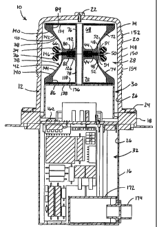
As shown in Figs. 1-3, the anti-collision light 10 includes a housing 12
composed of upper housing member or cover 14, a lower housing member or
case 16, and a mounting plate 18 disposed between the cover 14 and case 16.
The cover 14 is transparent and preferably has a Fresnel lens 20 integrally
formed therein. The cover, which may also be provided with a conventional
lo drain plug 22, is secured to the top side of the mounting plate 18 by a
hold-down
ring or lens bezel 24. The case 16 is fastened to the underside of the
mounting
plate 18 by fasteners (not shown) or other suitable means. Together, the cover
14, case 16 and mounting plate 18 define an interior region 26 for containing
the
internal components of the light 10, which internal components generally
comprise a flashtube fixture assembly 28, a fixture base 30 and electrical
circuit
components 32 for supplying power to and controlling the flashtube fixture 28.
As seen in Fig. 3, the flashtube fixture assembly 28 includes two
flashtubes 34 and 36 and a common spool-shaped reflector 38. The reflector 38
includes upper and lower reflector half spool members 40 and 42 that are
axially
2o aligned and coupled together. The reflector 38 is coupled to the fixture
base 30
which, in tum, is fastened to the mounting plate 18.
The flashtubes 34 and 36, which are herein referred as a main or primary
flashtube and a spare or secondary flashtube 36, respectively, are
conventional
circular-shaped (annular) flashtubes that are disposed circumferentially
around
the waist (smallest diameter portion) of the spool-shaped common reflector 38
in
substantially parallel relation to one another. The main flashtube (or spare
flashtube) 34 can be either the upper or lower flashtube shown in the
illustrated
light. The flashtubes 34, 36 preferably are supported in spaced apart parallel
relationship, such as by respective centering spacers 44.
With additional reference to Fig. 4, the centering spacers 44 have central
disk portions 46 from which support arms 48 radiate. As shown, four
-5-
CA 02349601 2001-05-04
WO 00/27699 PCT/US99/26209 7
circumferentially equally-spaced apart support arms 48 may be provided for
each spacer. The radially outer ends 50 of the support arms 48 are contoured
to support the corresponding flashtube 34, 36 and each arm 48 may have a hole
52 and slot 54 therein for receipt of a wire (not shown) wrapped around the
flashtube 34, 36 to hold it to the support arm 48 and thus to the centering
spacer
44. Each centering spacer 44 is affixed to the narrower end of a corresponding
one of the upper and lower reflector halves 40 and 42 by suitable fastening
means such as screws 60. Other, or alternative, types of spacers may be
employed to support and maintain a spaced relationship between the main
io flashtube 34 and spare flashtube 36.
The upper and lower reflector halves 40 and 42 progressively decrease in
diameter (width) going from their axially outer ends to their axially inner
ends
that are butted together at the waist 66 of the hourglass shape reflector 38.
Each reflector member 40, 42 has an interior annular region (chamber) 68, 70
1s disposed between a radially outer wall 72, 74 and an interior center post
76, 78.
The interior annular chamber 68, 70 is closed at the axially inner end of the
reflector member 40, 42 by an axial end wall 80, 82 while the other end of the
reflector member 40, 42 has an opening 84, 86 through which a trigger inductor
assembly 88, 90 (Fig. 4) can be inserted into the interior region 68, 70. The
20 trigger inductor assembly 88, 90 includes a PTFE inductor housing 96, 98
containing a trigger inductor 100, 102. The trigger inductor 100, 102 is
electrically connected by leads (not shown) to terminal ends 104, 106 of the
corresponding flashtube 34, 36. The terminal end portions 104, 106 extend
perpendicularly to the plane of the otherwise annular flashtubes 34, 36. The
25 terminal end portions 104, 106 extend through an opening 108 (only one of
which is shown) in the radially outer wall 110, 112 of the reflector half 40,
42 and
into the interior region 68, 70. After the electrical connections have been
made,
preferably the terminal ends 104, 106 and trigger inductor assemblies 88, 90
are
potted into their respective interior region 68, 70 with a suitable potting
30 compound.
-6-
CA 02349601 2001-05-04
WO 00/27699 PCT/US99/26209
Together each flashtube 34, 36, reflector half 40, 42 and trigger inductor
assembly 88, 90 form a respective light module 114, 116. In the illustrated
embodiment the light modules 114 and 116 are substantially identical except
for
their electrical connections. The trigger inductor module 90 and flashtube 36
of
the lower light module 116 are electrically connected to a printed circuit
board
118 fixed to the bottom (axially outer) end of the reflector half 42. The
bottom
printed circuit board 118 is provided with pins 120 to form a plug that mates
with
a corresponding socket (not shown) in the fixture base 30.
The bottom printed circuit board 118 also has through pins connected to
lo an upper printed circuit board 126 at the axially inner end of the lower
light
module 116. The upper printed circuit board 126 is provided with pins 128 for
mating with sockets provided on a printed circuit board 132 fixed to the
bottom
(axially inner) end of the upper light module 114. The sockets are
electrically
connected to the trigger inductor module 88 and flashtube 34, and any other
supporting electrical circuitry may be provided on a printed circuit board 134
fixed to the top (axially outer) end of the upper light module 114.
With the foregoing preferred construction of the light fixture 28, the light
fixture 28 is assembled by plugging the upper and lower modules 114, 116
together and the lower module 116 to the fixture base 30. When thus
2o assembled, the upper and lower light modules 114 and 116 may be held
securely together and to the fixture base 30 by a bolt (not shown) that
extends
through the center tube 76, 78 and has its lower end threaded into the fixture
base 30, such as into a nut fastener attached to the underside 136 of the top
wall 138 of the fixture base 30 or by any other suitable means.
In view of the foregoing, it can be seen that the modular construction of
the light 10 facilitates replacement of a defective and/or worn out module
114,
116, as well as assembly of the light fixture 28 in the first instance.
Together,
the joined upper and lower light modules 114, 116 form the reflector 38 that
is
shared by and thus common to the two flashtubes 34 and 36.
The reflector 38 has an outer annular concave reflective surface 140 for
reflecting light emitted by either one of the flashtubes 34, 36 substantially
-7-
CA 02349601 2001-05-04
WO 00/27699 PCT/US99/26209
radially (ho(zontally) outwardly to provide 360 degree horizontally
concentrated
illumination. Preferably, the reflective surface 140 has upper and lower semi-
parabolic shaped half surface portions 142 and 144 respectively formed on the
upper and lower reflector halves 40, 42. The focal points of the half portions
142, 144 preferably are axially spaced apart such that the main flashtube 34
can
be positioned at one focal point and the spare flashtube 36 can be positioned
at
the other focal point. Because of the annular nature of the reflector 38 and
flashtubes 34, 36, the focal points are actually focal lines with which the
annular
axes of the flashtubes 34, 36 are aligned. Most preferably, the semi-parabolic
lo shaped half surface portions 142 and 144 each extend slightly beyond the
center plane 146 of the respective parabola but not so far as to shade any of
the
reflective surface from light emitted from either flashtube 34, 36. Although
the
focal points of the two half surface portions 142, 144 are spaced apart, they
are
sufficiently close to reflect and focus light emitted not only from the
closest
flashtube 34, 36 but also the furthest flashtube 34, 36.
As will be appreciated, the light rays passing from a flashtube 34, 36 to
the nearest half surface portion 142, 144 of the reflector 38 will be
reflected so
as to pass generally radially away from the reflector 38 to provide a
horizontally
concentrated light pattem. However, the light rays passing from a flashtube
34,
2o 36 to the furthest half surface portion 142, 144 will be outwardly
divergent from
the horizontal because the flashtube 34, 36 is oppositely spaced from the
focal
point of such furthest half surface 142, 144. In those applications where it
is
desirable to concentrate the light intensity within a specified angle from
horizontal, such as 5 degrees for an aircraft recognition/anti-collision
light, the
cover 14 may be provided with a Fresnel lens 20 (other suitable lens means or
equivalent) to redirect the otherwise wayward rays into the desired horizontal
window.
As seen in Fig. 3, the Fresnel lens 20 differs from the classical Fresnel
lens by having two convex lens 148, 150 at the center with prisms 152, 154
so above and below. The two convex lens 148, 150 are respectively horizontally
aligned with the flashtubes 34, 36. In essence, each flashtube 34, 36 has
-8-
CA 02349601 2001-05-04
WO 00/27699 PCT/US99/26209 ~
associated therewith a parabolic reflector 142, 144 and Fresnel lens 20,
except
that the portion of each such reflector 142, 144 and lens 20 that would
interfere
with the other is removed and the two brought together along a center plane
146
equal spaced from the horizontal planes of the flashtubes 34, 36. Of course,
s other shaped reflector surfaces 140 and/or lens 20 may be employed to
provide
other light patterns that may be desired for various applications.
As depicted in Fig. 2, the flashtube fixture 28 is provided with a light pipe
(or other suitable light transmission means) 156 that extends from an aperture
158 located in the wall 74 of the reflector 38 and through an aperture 160 in
the
io top wall 138 of the fixture base 30. Within the base 30, the light pipe 156
extends to a light detector 162, such as a photodiode, mounted on a printed
circuit board constituting one of the electrical circuit components 32 (Fig.
3).
The light pipe 156 attenuates and conveys light emitted by each flashtube 34,
36 to the photodiode 162 for monitoring of light intensity in the hereinafter
15 described manner. The light intensity is monitored for the purpose of
controlling
the operation of light in the following preferred manner. Preferably, the
light pipe
156 functions to calibrate the light attenuation as necessary for linear
operation
of the photodiode 162.
In operation, initially the main flashtube 34 is flashed at a desired
20 frequency, such as at 42 flashes per minute which is within the flash rate
range
(40 to 100 fpm) mandated by FAA regulations for aircraft operation. The
intensity of the flashtube 34 is monitored, preferably continuously, by the
photodiode 162 and associated monitoring circuitry 32. If the measured
intensity is found not to be in compliance with a predetermined criteria, for
25 example the measured intensity falls below a minimum specified light
intensity,
such as the 100 candela mandated by FAA regulations, power to the main
flashtube 34 is boosted. This "power boost" mode causes the main flashtube 34
to continue flashing above the FAA minimum effective intensity. Although this
process can be repeated multiple times, preferably the power to the main
3o flashtube 34 is boosted only one time instead of incrementally.
-9-
CA 02349601 2001-05-04
WO 00/27699 PCTIUS99/26209
During the main flashtube power boost mode, continuous monitoring of
intensity of the main flashtube 34 continues until once again the measured
intensity is found not to be in compliance with a predetermined criteria, for
example the measured intensity falls below a minimum specified light
intensity,
such as the 100 candela mandated by FAA regulations. At this point, flashing
of
the main flashtube 34 is stopped and in its place the spare flashtube 36 is
flashed. Now it is the intensity of the spare flashtube 36 that is monitored:
If the
measured intensity falls below the minimum specified light intensity
threshold,
power to the spare flashtube 36 is boosted. This "power boost" mode causes
lo the spare flashtube 36 to continue flashing above the FAA minimum effective
intensity.
During the spare flashtube power boost mode, continuous monitoring of
intensity of the spare flashtube 36 continues until once again the measured
intensity is found not to be in compliance with a predetermined criteria. At
this
point the spare flashtube 36 is caused to flash at a different rate to provide
an
indication that the light is close to the end of its useful life. For example,
the
spare flashtube 36 may be caused to flash at twice its normal frequency.
Although changing the flash rate provides an effective way of indicating a
need
to service the light, other indicating means may be employed such as providing
2o an indicator light on the light unit, supplying a warning signal to the
aircrafts
control system for appropriate processing, such as display on a panel or
screen
in the cockpit, storing an indicator warning in memory for read-out by
diagnostic
equipment, etc.
The foregoing describes a preferred sequence of operation of the main
and spare flashtubes 34 and 36. However, it should be appreciated that the
sequence may be varied and/or portions thereof used in conjunction with a(ight
having more or less flashtubes. For example, the power boost feature may be
used with a single flashtube light to extend the useful life of the light.
Also, the
first and second flashtubes 34, 36 may be sequentially cycled through their
ao normal power modes first, and then cycled through their power boost modes.
Moreover, the first and second flashtubes 34, 36 may be altemately flashed
-10-
CA 02349601 2001-05-04
WO 00/27699 PCT/US99/26209
according to some specified criteria, such as altemately for a specified
period or
number of flashes. For example, the main flashtube 34 may be flashed for 1000
flashes, then the spare tube for 1000 flashes, then the main tube for 1000
flashes, and so on. Should either tube's light output intensity fall below the
minimum, it may be operated in the power boost mode, no longer operated, or
flashed at a different rate to indicate a need for servicing.
The above described operation of the anti-collision light 10 is effected by
the electrical circuitry 32, the functional components of which are
illustrated by
the functional block diagrams of Figs. 5 and 6. The electrical circuitry 32
io according to a preferred embodiment of the invention generally comprises
power
supply circuitry generally indicated at 164 in Fig. 5, and control and
monitoring
circuitry generally indicated at 166 in Fig. 6, respectively.
Referring principally to Fig. 5, the power supply circuitry 164 includes an
EMI filter 168 to which input power is routed, such as 115 VAC provided on an
aircraft. The EMI filter 168 attenuates noise generated in a power supply 176
from being coupled on the aircraft power line. The EMI filter 168 also
suppresses noise on the power line that could affect the operation of the
power
supply. The EMI filter 168 may be housed in an EMI can 172 provided in the
housing 12 and equipped with an extemal power connector 174 as shown in Fig.
2o 3.
The filtered power is used to power the circuits of the power supply 176.
The power supply 176 includes a transistor AC switch 177 which controls the
filtered AC power that is used for charging flash capacitors 178. A preferred
switch consists of two FET transistors in an AC bridge configuration that has
slow tum-on to reduce in-rush current when the flash capacitors 178 start to
charge. The transistor on/off control may be provided by an isolated switch
control circuit 180 that takes low voltage control signals that are referenced
to
ground and converts them to control signal referenced to 115 VAC. A voltage
doubler circuit 179 converts the 115 VAC to approximately +280 VDC and -280
so VDC for use as capacitor charging voltages. The voltage doubler 179 is
capable
-11-
CA 02349601 2001-05-04
WO 00/27699 PCT/US99/26209
of producing 320 VDC from 115 VAC. The actual voltage developed is controlled
by the power regulator 190 and can vary between 250 VDC and 295 VDC.
The flash capacitors 178 are used to supply the energy used by the
flashtube 34, 36. In a preferred embodiment, four capacitors may be arranged
in
two parallel sets that are connected in series. The flashtube 34, 36, which
may
be a xenon gas flashtube, is connected across the series connected capacitors
and provides a desired voltage of about 500 to 600 volts, for example, to the
flashtube 34, 36.
More particularly, the anode and cathode of each flashtube 34, 36 is
,o connected to the outputs of the capacitors 178. In a preferred arrangement,
the
cathode of each tube 34, 36 is connected to the minus capacitor through the
secondary winding of the trigger inductor 100, 102 (transformer). The primary
winding of the trigger inductor 100, 102 is connected to a respective
flashtube
trigger generator circuit, there being a main flashtube trigger generator
circuit
186 for the main flashtube 34 and a spare flashtube trigger generator circuit
188
for the spare flashtube 36. When a trigger pulse, for example a -275 volt
pulse,
is applied to the primary winding of the trigger transformer, a high voltage
negative pulse, for example -5000 V to -7000 V, is developed by the
transformer
secondary winding. This voltage causes the xenon gas in the flashtube 34, 36
to
change from an insulator to a low resistance conductor, whereupon the flash
capacitors 178 discharge through the flashtube 34, 36 creating a brilliant
white
flash of light. A grounded wire may be wrapped around the outside of the
flashtube 34, 36 to help propagated the ionization gas in the flashtube 34, 36
and
provide shielding for EMI generated by the flashtube 34, 36 when it fires.
This
minimizes cross-talk between the main and spare flashtubes 34, 36. Also, this
method of triggering the flashtubes 34, 36 provides several other advantages.
In
particular, it permits the flashtubes 34, 36 to be mounted in close proximity
to
one another in stacked relationship which, in turn, allows the common
reflector
38 to be used for both flashtubes 34, 36. As a consequence, the optical design
so of the reflector 38 and lens 20 is greatly simplified. Another advantage is
that
series trigger circuits provide trigger voltage isolation between flashtubes
34, 36
-12-
CA 02349601 2001-05-04
WO 00/27699 PCT/US99/26209
so that trigger coupling between the closely spaced flashtubes 34, 36, which
typically causes erratic flashing in parallel trigger circuits, is prevented.
The
series trigger circuit also provides electromagnetic shielding for the
flashtubes
34, 36 which reduces electromagnetic interference (EMI) that the flashtubes
34,
36 are exposed to during initial triggering. It also reduces the amount of EMI
suppression required to meet FAA imposed EMI requirements.
The charging of the flash capacitors 178 is controlled by a power regulator
190. After a flashtube 34, 36 fires and the flash capacitors 178 are
discharged,
the regulator 190 receives a timing signal from a flasher timer 192 to start
lo charging the capacitors 178. The regulator 190 supplies a signal to the
isolated
switch control 180 that is used to turn-on the transistor AC switch 179,
starting
the charging cycle. After the capacitors 178 have been charged to the voltage
needed to obtain the required power, the power regulator 190 turns off the
signal
to the isolated switch control 180 which tums off the AC power to the flash
capacitors 178. As the capacitors 178 age and their capacitance changes, the
power regulator 190 adjusts the capacitor charging voltage to keep the power
output constant, which output is a function of the flash capacitor capacitance
and
the capacitor voltage. This keeps power at a minimum level and extends the
life
of the flashtube 34, 36. When the flashtube intensity decreases below the
minimum threshold, an intensity monitor power boost latch 194 (Fig. 6) sends a
signal to the power regulator 190 to increase the power to the flashtube 34,
36.
This will increase the intensity and provide additional operating time for the
flashtube 34, 36 as was discussed above.
The regulator 190 preferably has associated therewith an over voltage
monitor 196 that measures the positive and negative flashtube voltages. If the
charging voltage increases above a specified amount, for example, plus or
minus
300 VDC, the over voltage monitor 196 overrides the power regulator 190 with a
turn-off signal to the isolated power control circuit 180. This would occur,
for
example, if the flashtube 34, 36 does not fire. In such event, the power
regulator
190 would attempt to charge the already charged capacitors 178 and would, if
-13-
CA 02349601 2001-05-04
WO 00/27699 PCT/US99/26209
not stopped by the overvoltage monitor 196, overcharge the capacitors 178, and
this may reduce their useful life.
As further shown in Figs. 5 and 6, the electrical circuitry includes a sync
circuit 198 that supplies a sync signal, for example a 400 Hz signal, to the
flasher
timer 192. This signal is used to control all timing functions in the power
supply
176 via the flasher timer 192 which generates timing signals required by the
power regulator 190 and the trigger generators 186, 188. The timer 192 also
generates a timing signal for control of an intensity monitor circuit 200 that
is
discussed below. The trigger generators 186, 188 are capable of producing a
io flashtube trigger at a normal rate of 42 flashes per minute for example,
and at
least the spare trigger generator 188 is capable of producing a flashtube
trigger
at a different rate such as twice the normal rate or a double flash trigger
signal.
The power for the flashtube triggers 186, 188 is provided by a trigger
power circuit 202. The trigger power circuit 202 may be a positive voltage
doubler for supplying 300 VDC to the flashtube trigger generators 186, 188.
Each flashtube generator 186, 188 produces, for example, a -275 volt pulse
that
is connected to the trigger coil of the trigger transformer 100, 102 for the
flashtube 34, 36. The pulse may be generated by a capacitor discharge SCR
circuit that is controlled by the lamp intensity monitor trigger control
circuit 204,
2o 206. If the flashtube 34 fails to fire, the capacitor voltage will be at a
steady
value, either low or high depending on the cause of the flash not firing. A
flash
detector 207 monitors the charging and discharging of the flash capacitors
178.
If they are at a steady voltage and not being charged and discharged for a
predetermined time period, the flash detector 207 generates a fail signal that
is
sent to a main flashtube fail latch 208 to initiate the switching to the spare
flashtube 36. Similarly, the spare flashtube generator 188 produces, for
example, a -275 volt pulse that is connected to the secondary trigger coil of
the
trigger transformer 102 for the spare flashtube 36. The pulse may be generated
by a capacitor discharge SCR circuit that is controlled by a spare lamp
intensity
monitor trigger control circuit 206.
-14-
CA 02349601 2001-05-04
WO 00/27699 PCT/US99/26209 LL
As further seen in Fig. 5, the power supply 176 further comprises a low
voltage power supply 209 for supplying low DC voltage to the flasher power
supply circuit and intensity monitor circuit. The low voltage power supply 209
may include a transformer that steps the 115 VAC down to the desired DC
voltages such as t10 VDC and 5 VDC. The transformer may also have an
isolated winding that provides power to the isolated switch control circuit
180.
Referring now principally to Fig. 6, the intensity monitor and control circuit
166 includes a photodiode circuit 210 including the photodiode 162 which as
above noted continuously monitors the light intensity of the operating
flashtube
,o 34, 36 via the light pipe 156. The photodiode circuit 210 provides an
output
signal to an integrator circuit 212 that is proportional to the light
intensity
generated by the then operating flashtube 34, 36. As is preferred, the
photodiode 162 is selected to produce a response that approximates the
response of the human eye and to quantify the light intensity in candela, a
i s photometric measurement allowing the intensity to be compared to
requirements
for FAA approved intensity photometric test measurements. The photodiode 162
should also be capable of providing a stable output over the full operating
temperature range of the flashtubes 34, 36. If the output of the photodiode
circuit 210 or altemative light sensor is temperature sensitive, then
temperature
20 compensation could be provided to provide a normalized output. As is
preferred,
the photodiode 162 may be packaged in a metal hermetically sealed case with a
glass window for environmental protection.
The integrator circuit 212 converts the measured light intensity provided
by the photodiode circuit 210 into an integrated output voltage which is a
function
25 of the light intensity of the flash emitted by flashtube 34, 36. Since the
light
intensity of the flashes typically varies by a small amount, the light from
multiple
flashes is integrated to obtain an average intensity. Averaging the light
intensity
from multiple flashes provides a more stable signal for the determination of
the
actual light intensity output and prevents a false lamp fail signal from being
30 generated as a result of occasional sub-threshold flash. Each time the
flashtube
34, 36 flashes, the integration output voltage will increase by an amount
-15-
CA 02349601 2001-05-04
WO 00/27699 PCT/US99/26209
proportional to the intensity of the flash. Thus, the voltage obtained at a
particular time is equal to the total voltage of all the flashes measured up
to that
particular time. Thus, the output signal of the integrator 212 is a DC voltage
proportional to the average intensity of the light output. After a prescribed
number of flashes have been integrated, the output of the integrator 212 is
compared by an intensity comparator 214 against a reference value provided by
a reference voltage source 216 and then the integrator 212 is reset (to zero)
by
the intensity monitor counter 200 before measuring a next series of flashes.
The intensity comparator 214 monitors the output of the integrator 212
io and produces an output indicative of whether the integrator 212 output
satisfies
or does not satisfy the comparison criteria. In the illustrated embodiment,
the
comparator 214 produces a GO or NOGO signal based on a comparison of the
integrator 212 output signal to a reference voltage preferably supplied by the
reference voltage source 216 which may be a stable temperature compensated
voltage circuit. The reference voltage level may be set in relation to the
FAA's
minimum effective light intensity requirement, for example to correspond to
the
FAA's minimum effective light intensity requirement or slightly above such
minimum requirement. If the integrator 212 output voltage is less than the
reference voltage, the comparator 214 outputs a NOGO signal. If the integrator
2o 212 output voltage is greater than the reference voltage, the comparator
214
outputs a GO signal.
Initially the integrator 212 output voltage will be below the comparator
reference voltage and the comparator 214 will output a NOGO signal. As
consecutive light flashes are measured, the integrated output voltage will
gradually increase from zero volts to the final voltage measured for the
prescribed number of flashes. When the integrator 212 output voltage rises
above the reference voltage, the comparator 214 will output a GO signal. If
the
intensity of the flashtube 34, 36 decreases below the minimum limit, the
comparator output will stay in a NOGO state.
After a set of flashes have been measured, the state of the comparator
output is stored in an intensity status latch circuit 220 which is controlled
by the
-16-
CA 02349601 2001-05-04
WO 00/27699 PCT/US99/26209
intensity monitor counter circuit 200. The intensity monitor counter 200 is
clocked by the flasher timer 192 and provides timing signals not only for the
intensity status latch 220, but also for the integrator 212, a light warm-up
inhibit
latch 222 and an intensity integrator fail counter 226. At power turn-on the
counter is set to zero by a power-on reset circuit 225 and synchronizes the
operation of the counter.
After the intensity monitor counter 200 counts the prescribed number of
flashes for a set of flashes to be integrated for comparison to the reference
value, the counter 200 sends a clock signal to the intensity status latch 220
to
lo have it store the GO/NOGO state of the intensity comparator output. This
occurs
shortly before the counter 200 resets the integrator 212, setting it to
measure
another set of flashes. The latch 220 then ignores the comparator output until
the next set of multiple flashes is measured and another clock signal sent by
the
counter 200 to the intensity status latch 220.
Preferably the intensity status latch 220 is inhibited from outputting a
NOGO signal for a preset period of time after the then active flashtube 34, 36
has been tumed on. This allows the flashtube 34, 36 to warm up to its
operating
temperature. Under some low temperature conditions, the light intensity of the
flashtube 34, 36 may be below the required intensity in which case a NOGO
signal would be outputted by the comparator 214 and captured by the intensity
status latch 220 when, after a warm-up period, the light intensity would
otherwise
rise above the required minimum. An inhibit signal may be supplied from latch
222 to the intensity status latch 220 for the prescribed period governed by
the
intensity monitor counter 200, that is, the time period may be based on a
number
of flashes needed to bring the flashtube 34, 36 up to its operating
temperature.
The GO/NOGO status of the intensity status latch 220 is monitored by an
intensity integrator fail counter circuit 226. The intensity integrator fail
counter
226 prevents premature switching of the main flashtube 34 to the spare
flashtube
36 when the light intensity of the main flashtube 36 approaches the minimum
light intensity. Since the decrease in light intensity usually is gradual,
light output
may intermittently fall below the specified minimum light intensity. The
intensity
-17-
CA 02349601 2001-05-04
WO 00/27699 PCTIUS99/26209
integrator fail counter 226, which is clocked by the intensity monitor counter
200,
monitors the intensity status latch 220 for a predetermined number of
consecutive NOGO output signals corresponding to consecutive multiple sets of
flashes. If the prescribed number of consecutive measurements are NOGO, the
intensity integrator fail counter 226 provides a fail signal in the form of a
power
boost latch set signal to the power boost latch 194 which enables the power
boost mode of the power regulator 190. In response, the power regulator 190
increases the voltage to which the flash capacitors 178 are charged. The
increased voltage corresponds to an increase in the light intensity of the
main
io flashtube 34. This, in effect, extends the useful of the main flashtube 34.
Moreover, this extends the lifetime of the main flashtube 34 beyond the life
the
main flashtube 34 would otherwise have had if operated at the higher voltage,
as
the lifetime of a flashtube typically decreases with increasing operating
voltage.
After the power to the main flashtube 34 is boosted, the intensity
integrator fail counter 226 continues to monitor the GO/NOGO status of the
intensity status latch 220. If several consecutive measurements are NOGO, the
intensity fail counter 226 provides a main lamp fail signal to a main lamp
fail latch
208 for initiating switching to the spare flashtube 36. The main lamp fail
latch
208 provides an inhibit signal to the main lamp trigger control 204 and an
enable
signal to the spare lamp trigger control 206 (during operation of the main
flashtube 34 the main lamp fail latch 208 outputs an inhibit signal to the
spare
lamp trigger 206 to prevent the spare flashtube 36 from flashing). The main
lamp
fail latch 208 also provides a reset signal to the power boost latch 194 which
causes the power regulator 190 to charge the flash capacitors 178 to the
original
-25 or normal power settings. The spare flashtube 36 will now be flashed in
place of
the main flashtube 34.
During flashing of the spare flashtube 36, the intensity integrator fail
counter 226 continues to monitor the GO/NOGO status of the intensity status
latch 220 and the output of the intensity integrator fail counter 226 is sent
to a
ao spare lamp fail latch circuit 228. If several consecutive measurements are
NOGO, the intensity integrator fail counter 226 provides a lamp fail signal to
the
-18-
CA 02349601 2001-05-04
WO 00/27699 PCT/US99/26209
power boost latch 194 which enables the power boost mode of the power
regulator 190. In response, the power regulator 190 increases the voltage to
which the flash capacitors 178 are charged. The increased voltage corresponds
to an increase in the light intensity of the spare flashtube 36. This, in
effect,
extends the useful life of the spare flashtube. Moreover, this extends the
lifetime
of the spare flashtube beyond the life the spare flashtube would otherwise
have
had if operated at the higher voltage.
After the power to the spare flashtube 36 is boosted, the intensity
integrator fail counter 226 continues to monitor the GO/NOGO status of the
lo intensity status latch 220. If several consecutive measurements are NOGO,
the
intensity fail counter 226 provides a spare lamp fail signal to the spare lamp
fail
latch 228 which sends a double flash enable signal to the spare lamp trigger
206.
The spare flashtube 36 is then double flashed to provide a visible indication
to
the air crew and/or ground maintenance personnel that the intensity of the
light is
near the FAA minimum level. In the preferred embodiment, the spare flashtube
36 flashes at 84 flashes per minute, which is twice the 42 flashes per minute
in
normal operation. Preferably, during double flashing, every other flash is
generated at reduced power to limit the total power to the flashtube to a
level that
will not cause the flashtube to overheat and burn- out. Notably, both the
normal
(42 FPM) and the double (84 FPM) flash rate fall within the FAA's acceptable
flash rate range. The "double flash" rate alerts aircraft maintenance
personnel
that the light intensity of the anti-collision light 10 is near the minimum
required
effective intensity and that servicing of the anti-collision light 10 is
required. The
spare flashtube 36 will continue to double flash until repaired or replaced.
As is
preferred, battery power is provided when the light 10 is turned off to retain
the
low intensity status until power is reapplied.
After both lamps have reached their end-of-life, it may be desirable to
flash both lamps simultaneously to generate sufficient light output from the
light
fixture. This may require some redundancy such as two sets of flash
capacitors.
An operating hours counter circuit 230 counts the number of flashes that
have been accumulated by the flashtubes 34, 36. The counter 230 is clocked by
-19-
CA 02349601 2001-05-04
WO 00/27699 PCT/US99/26209
the flasher timer 192 and increments each time a flashtube 34, 36 fires. As is
preferred, the counter 230 is powered from battery power and retains its count
when the light 10 is not powered. In a preferred embodiment, the counter 230
is
capable of recording about 26,000 hours of operation (about 67 million
flashes)
and can only be reset during maintenance when the flashtubes 34, 36 are
replaced.
Although the invention has been shown and described with respect to
certain preferred embodiments, equivalent alterations and modifications will
occur to others skilled in the art upon reading and understanding this
lo specification and the annexed drawings. In particular regard to the various
functions performed by the above described integers (components, assemblies,
devices, compositions, etc.), the terms (including a reference to a "means")
used
to describe such integers are intended to correspond, unless otherwise
indicated,
to any integer which performs the specified function of the described integer
(i.e.,
that is functionally equivalent), even though not structurally equivalent to
the
disclosed structure which performs the function in the herein illustrated
exemplary embodiment or embodiments of the invention. In addition, while a
particular feature of the invention may have been described above with respect
to only one of several illustrated embodiments, such feature may be combined
with one or more other features of the other embodiments, as may be desired
and advantageous for any given or particular application.
-20-