Note: Descriptions are shown in the official language in which they were submitted.
CA 02350075 2001-05-07
WO OO/Z8798 PCTNS99I26Z55
METHOD OF MANUFACTURING AN INTERLAYER VIA AND A LAMINATE
PRECURSOR USEFUL FOR SAME
CA 02350075 2001-05-07
WO 00/28798 PCT/US99/26255
BACKGROUND OF THE INVENTION
1. Field of the Invention
This invention includes a metal-clad laminate product that may be associated
with a
substrate wherein the metal-clad laminate product includes a semi-transparent
metal layer that
is thin enough to allow actinic light to penetrate the semi-transparent metal
layer and reach
into a photo dielectric layer below. This invention also includes a method for
manufacturing
circuit board having interlayer vias using metal clad laminates including a
semi-transparent
metal layer.
2. Description of the Related Art
The electronics industry continues to seek enhanced product performance in
order to
meet consumer demands for higher functionality and lower cost computers and
electronics
equipment. Among the methods that the electronic industry is using to increase
performance
is by the design of circuit boards that have smaller, finer circuit lines and
spaces. Increasing
line density leads to fewer circuit layers resulting in smaller electronic
devices. In addition,
the industry is also migrating towards built-up technologies using micro-vial.
Mufti layer
circuit boards using dielectric circuit layers connected by very small holes
(vias) significantly
densify the circuit due to reduced board area per hole.
Current circuit board designs require substrate materials on which extremely
fine lines
and spaces can be formed with a high degree of precision. Metal foils are
generally a preferred
substrate for the formation of circuit lines on circuit boards. The metal
films are most
commonly formed by electrodeposition. Electrodeposited copper films typically
must be of a
defined minimum thickness, >1 ~.m, to avoid holes or discontinuities. Metal
foils that are
currently in use in the industry are typically at least 5 ~.ms in thickness.
The use of thinner
metal foil in printed circuit board would allow the formation of more densely
packed lines and
would reduce production costs. Thus, there is a significant interest in
developing methods for
2
CA 02350075 2001-05-07
WO 00/28798 PCT/US99/Z6255
obtaining thin copper foils. Existing methods for obtaining and placing a very
thin metal foil
on a laminate are limited. One example of methods for using thin metal layer
articles of
manufacture to prepare printed circuit board layers is disclosed in U.S.
Patent Application
Serial No. 09/075,732, which is incorporated herein by reference.
Photovia processes, which use photoimageable dielectric materials to fabricate
builtup
multilayer printed circuit boards, have been developed. In these processes,
photo dielectrics
are coated on a patterned core and photoimaged to define via holes. The via
holes along with
the surface of the dielectric layer are then plated with copper. U.S. Patent
5,354,593
sequentially laminates and photoimages two photo dielectrics onto a conductive
core to define
via holes and then copper plates the via holes. U.S. Patent 5,451,721 produces
a multilayer
printed circuit board by applying a photosensitive resin layer onto a core
having a metal line
on its surface. After imaging to form vias, the resin layer is deposited with
a copper layer by
electroless plating techniques. U.S. Patent 5,334,487 produces a patterned
layer on a substrate
by applying and exposing different photosensitive compositions on opposite
sides of a copper
foil. One side is developed and the copper etched, followed by developing the
other side and
metallization of through holes. U.S. Patents 5,354,593, 5451,721 and 5,334,487
are each
incorporated herein by reference.
Current high density built-up technologies largely depend on via holes and
dielectric
layers metallized by sputter metal deposition or electroless seeding. Via
formation can occur
by reactive ion etching, photolithography in the case of photo reactive
dielectrics, wet etching,
or projection ablation. Photo dielectrics are becoming the most attractive
approach due to
their fit with current printed wiring board equipment. The subsequent metal
layer, being
sputtered or electroless deposited, is applied as a seed layer for pattern
plating or panel plating
circuit formation. Sputter deposition is preferred due to the dry processing,
but current printed
wiring board infrastructure does not contain sputtering technology, and the
technology is
3
CA 02350075 2001-05-07
WO 00/28798 PCT/US99/26255
limited to small printed wiring boards. Examples of methods and articles of
manufacture
useful for preparing circuit boards including interlayer vias are disclosed in
U.S. Patent
Application Serial Nos. 09/054,264, and 09/054,263 each of which are
incorporated herein
by reference. Electroless seeding is possible in many board processes, but the
steps require
board exposure to severe a pH wet process and give seed layers of poor
uniformity, with low
conductivity and residual metals trapped within the dielectric after etching.
As a result, there
is a need for technology that enables via formation with high density circuits
that fits many of
the current wiring board processes.
4
CA 02350075 2001-05-07
WO 00/28798 PCT/US99/26255
BRIEF SUMMARY OF THE INVENTION
An object of the present invention is to provide a metal-clad laminate for use
in
manufacturing printed circuit boards including interlayer vias.
Another object of the present invention is to provide a method for
manufacturing a
prepeg and/or circuit board including at least one interlayer via that uses a
single photo
imaging step.
The present invention involves a metal-clad laminate product that includes a
cattier
film having a first surface and a second surface, a release agent layer
covering the carrier film
first surface, a conductive metal layer including at least one conductive
metal deposited onto
the release agent layer and having a thickness of from about 50 to about 3000
angstroms, a
photo dielectric layer, and an optional adhesion layer deposited on the
conductive metal layer.
The present invention also involves a method of manufacturing an interlayer
via. The
interlayer via is made by preparing a circuit board intermediate that includes
(1) a substrate;
(2) a photo dielectric layer deposited on the substrate; (3) an semi-
transparent metal layer; and
(4) at least one embedded circuit. The interlayer via is formed by exposing at
least a portion
of the circuit board intermediate to light through the semi-transparent metal
layer for a period
of time sufficient to form an exposed photo dielectric portion and an
unexposed photo
dielectric portion. Following a single exposure to a light source the exposed
or unexposed
portion of the photo dielectric layer and a corresponding portion of the semi-
transparent metal
layer overlying the exposed or exposed portion of the photo dielectric layer
is removed to
farm a via.
5
CA 02350075 2001-05-07
pC1'/US99I26255
WO 00/28798
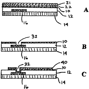
BRIEF DESCRIPTION OF THE FIGURES
Figures lA, 1B, 1C, 1D, and lE depict a cross-sectional illustration of a
circuit board
intermediate product during the steps of a prior art method for manufacturing
a circuit
including interlayer vias;
Figures 2 and 3 are cross-sectional illustrations of a metal clad laminate
product and a
circuit board precursor substrate including at least one embedded circuit
prior to the union of
the two layers;
Figure 4 is a cross-sectional illustration of a circuit board intermediate
product that
results from the combination of the two layers depicted in the Figure 2; and
Figures SA, SB and SC depict a cross-sectional illustration of a circuit board
intermediate product during steps of a method for manufacturing interlayer
vias in a circuit
board.
DETAILED DESCRIPTION OF THE INVENTION
Figtue 1 depicts steps of a prior art method for manufacturing a printed
circuit board
including at least one embedded circuit. The method, which is described in
detail in U.S.
patent application Serial Nos. 09/054,263 and 09/054,264, which are
incorporated herein by
reference, begins with a layered laminate, shown in Fig. lA, including a
conductive metal
layer 110, a photo dielectric layer 112, a base layer 114, and at least one
embedded circuit
116. A resist layer 130 is applied to the conductive metal layer as shown in
Fig. 1B. The
resist layer 130 is exposed to actinic light and resist layer 130 is developed
to expose portions
of conductive metal layer 110. The exposed conductive metal layer 110 is
etched from the
substrate to give a partial via 132' as shown in Fig. 1C. In the case of
positive acting photo
dielectric materials, the laminate is exposed a second time to actinic light
to soften the photo
dielectric layer portion located in partial via 132' after which the exposed
photo dielectric
layer portion is removed to forrrt via 132 that exposes at least a portion of
embedded circuit
6
CA 02350075 2001-05-07
pC'f/US99I26255
WO 00/28798
116 as shown in Figure 5C. Finally, An interconnect 140 is applied to via 132
and conductive
metal layer 110 by panel or pattern plating methods known in the art in order
to electrically
unite embedded circuit 116 with conductive metal layer 110.
Figure 4 depicts a circuit board intermediate product that is useful for
manufacturing
interlayer vias. The circuit board intermediate product comprises a semi-
transparent metal
layer 10, which is associated with a photo dielectric layer 12, which in turn
rests upon a base
14. The intermediate product includes at least one integral circuit 16
consisting of a
conductive material such as a metal.
Figure 2 is a cross-section of a metal-clad laminate products useful for
manufacturing
the intermediate product shown in Figure 4. Metal clad laminate 50 is located
above substrate
60 which includes a base layer 14 and at least one embedded circuit 16. Metal
clad laminate
50 includes a polymer or metal foil carrier layer 21, a polymeric release
agent layer 22 formed
on the carrier film, and a semi-transparent metal layer 10 formed on release
agent layer 22.
Metal-clad laminate 50 may optionally include an adhesion layer 24 that
facilitates adhesion
of the metal-clad laminate 50 to photo dielectric layer 12. Alternatively,
photo dielectric
layer 12 may be pre applied to base 14 of substrate 60 such that photo
dielectric layer 12
covers at least one embedded circuit 16. This alternative embodiment is
depicted in Figure 3.
Preferably, carrier layer2l comprises a flexible, dimensionally stable
material with
good tear and chemical resistances. Carrier layer 21 should be tolerant to
above-ambient
temperatures. Preferably, Garner layer 21 is made of a material having low
absorbed moisture
and residual solvent, because water and solvents can interfere with the
metallization step.
Suitable materials include polymeric film or metal foils. A metal foil is
preferred because
metal foils tend to have high tensile strength at elevated temperatures, low
absorbed moisture,
and low residual solvent.
7
CA 02350075 2001-05-07
WO 00/28798 PCT/US99I26255
Carrier layer 21 is preferably electroplated copper foil or a polyimide film.
Other
metal foils that would make suitable carrier films include rolled or
electrodeposited metal and
metal alloys including steel, aluminum (AllFoils available from Alcoa), and
copper available
from Gould Inc., and Oak Mitsui Inc. It is expected that certain polymeric
films would be
suitable for the practice of the present invention. Examples of suitable
polymeric films
include polyesters such as polyethylene terephthalate, poly-butylene
terephthalate and
polyethylene naphthalate (Kaladex~ available from ICI America), polypropylene,
polyvinyl
fluoride (Tedlar0 available from DuPont), polyimide (Kapton~ available from
DuPont;
Upilex~ available from UBE Industries), and nylon (Capran~ available from
AlliedSignal).
Release agent layer 22 is used to facilitate removal of Garner layer 21 from
semi-
transparent metal layer 10. In order to avoid the problem of picking, which
results in
incomplete transfer of semi-transparent metal layer 10 to the substrate under
lamination, the
release agent layer 22 is designed to peel at the interface between release
agent layer 22 and
carrier layer 21. Release agent layer 22 is subsequently removed from semi-
transparent metal
layer 10 with the aid of plasma, an oxidizing environment, intense light, or
an appropriate
solvent. Preferably, release agent layer 22 is removed by washing with a
solvent, most
preferably an aqueous solution. In methods that lack a release agent layer,
and in methods that
employ a release agent layer that peels at the interface between the parting
layer and the semi-
transparent metal layer, incomplete transfer of the metal of the semi-
transparent metal layer to
the substrate commonly occur.
Release agent layer 22 is made of a polymeric material. Preferably, the
release agent is
an aqueous-soluble material to facilitate its convenience removal from semi-
transparent metal
layer 10. Because photo resists are developed in an alkaline environment, it
would be most
preferable to use a release agent that is soluble in an aqueous alkaline
solution. A useful
polymer is one that is of a good film-forming material. The polymer can be
coated from water
8
CA 02350075 2001-05-07
PCTNS99I26255
WO 00/28798
with the aid of a volatile base such as ammonium hydroxide to aid solubility.
Optionally, the
release agent comprises a water-soluble surfactant to improve solution wetting
properties, and
to control drying defects.
A preferred release agent is applied as a formulation comprising a
polyvinylpyrrolidone (PVP) polymer, a surfactant, and water. It is expected
that formulations
containing PVP in the range of from about 1 % PVP to about 50% PVP, and
surfactant in the
range of from about 0% surfactant to about 5% surfactant are suitable for the
practice of the
present invention. Preferred PVPs for use in the present invention have a
molecular weight in
the range of about 10,000 to about 5,000,000. It is reasonable to expect that
a release agent
layer comprising a polymer such as acid modified acrylic polymers, acrylic
copolymers,
urethanes, and polyesters, carboxylic acid functional styrene acrylic resins
(S.C.Johnson Wax,
Jonc 1~), polyvinyl alcohols (Air Products & Chemicals, Airvol~), and
cellulose based
ry
polymers could be successfully employed in the practice of the present
invention. Other
suitable water soluble surfactants that are useful as the release agent layer
of the present
invention include alkylarylpolyether alcohols (Rohm & Haas, Triton~ X100),
glycerin,
ethoxylated castor oil (CasChem Inc., Surfactol~ 365), and fluoroaliphatic
polymeric esters
(3M Corporation. F7uorad~ 430). The release agent formulation is applied in an
amount
sufficient to achieve a dry weight of from about lOmg/ftz to about 1000mg/ft2,
about 0.1 p.m
to 10 ~tm. Preferably, the release agent formulation is applied in an amount
sufficient to
achieve a layer of about lp.m to 4 p.m in thickness with a dry weight of from
about 100mg1ft2
to about 400mg/ft-.
Release agent layer 22 is applied to carrier layer 21. Onto exposed release
agent layer
22 is deposited an semi-transparent metal layer 10. Semi-transparent metal
layer 10 may be
manufactured out of a single layer of conductive metal or out of multiple
layers of conductive
metals or alloys. Regardless of the number of layers used, it is important
that semi-transparent
9
CA 02350075 2001-05-07
WO 00/28798 PC'f/US99l26255
metal layer 10 is thin enough to be semi-transparent, i.e., thin enough to
allow at least some
light to pass through the semi-transparent metal layer 10 and into contact
with photo dielectric
layer 12. We have determined that a semi-transparent metal layer 10 having a
thickness of
from 10 Angstroms to about 3000 Angstroms is sufficiently thin to allow light
to penetrate
through the semi-transparent metal layer 10 and into photo dielectric layer
12. However, in
order to insure that the light is transmitted through semi-transparent metal
layer 10 at an
intensity sufficient to quickly react with the photo dielectric layer 12, it
is preferred that semi-
transparent metal layer 10 has a thickness of from about 50 to about 1000
Angstroms and
most preferably, a thickness of from about 100 to about 750 Angstroms.
Semi-transparent metal layer 10 may consist entirely of a thin primary
conductive layer
which is deposited onto release agent layer 22 by sputtering using a Desk III
sputtering unit. It
is expected that any sputtering or vapor deposition method known in the art
may be
successfully used in this invention. Semi-transparent metal layer 10 is
preferably
manufactured of gold, chrome, copper, or alloys thereof. Other suitable metals
may include,
but not limited to, tin, nickel, aluminum, titanium, zinc, chromium-zinc
alloy, brass, bronze,
and alloys of the same. Semi-transparent metal layer 10 may optionally be made
from a
mixture of suitable metals or non-metal conductive and non-conductive
materials.
Optionally, semi-transparent metal layer 10 may include a primary metal layer
and a
secondary metal layer with the secondary metal layer 10 being used to protect
the primary
layer from oxidation, to increase adhesion during lamination, or to act as a
barrier to metal
migration. To form the optional secondary metal layer, a layer of zinc,
indium, tin, cobalt,
aluminum, chrome, nickel, nickel-chrome, brass, or bronze are alloys thereof
is deposited on
the first metal layer. Other suitable metals include magnesium, titanium,
manganese, bismuth,
molybdenum, silver, gold tungsten, zirconium, antimony, and chromium-zinc
alloys. The
secondary metal layer prevents the metal in the first metal layer from
oxidizing after removal
CA 02350075 2001-05-07
PCT/US99126255
WO OOI28798
from the metallizing chamber, and increases adhesion to thermosetting resin
systems. The
total thickness of the primary and secondary metal layers of the semi-
transparent metal layer
must not exceed 3000 Angstroms, and preferably not greater than about 1000
Angstroms and
most preferably not exceed 750 Angstroms.
An optional adhesion layer 24 can be applied to the semi-transparent metal
layer 10.
Adhesion layer 24 is used to increase the bond between the metal layers and
the substrate
layers following lamination. Optional adhesion layer 24 may be organic,
organometallic, or
inorganic compounds, and applied to a thickness of 0.0005 ~cm (5 Angstroms) to
10 ~tm
( 100,000 Angstroms). Multiple layers may be used such as an organometallic
layer followed
by an organic layer. Typically when an organometallic layer is used, such as a
silane, the
coating will be from 0.0005 ~m (5 Angstroms) to 0.005 ~,m (500 Angstroms) in
thickness.
When using organic adhesion layers, such as thermoplastics, thermosetting
polymers, or
mixtures, the coating would be 0.1 ftm (1000 Angstroms) to 10 ~.m (100,000
Angstroms) in
thickness. The organic adhesion layer should be chosen so as to be soluble in
the solvent used
to develop the photo dielectric layer.
According to Figure 2, substrate 60 includes a base layer 14 on which is
located at
least one exposed embedded circuit 16. Base 14 may be any material useful in
manufacturing
printed circuit boards. Typically, the substrate base consists of a dielectric
material such as a
thermoplastic or thermoset film; composites with glass, ceramic, or organic
reinforcement; or
ceramics or metals.
Photo dielectric layer 12 may be any negative acting or positive acting resin
system
when exposed to an actinic light source. Examples of useful photo dielectric
materials
include epoxies, polyimides, and acrylate based resins. Compositions disclosed
in U.S. Patent
No. 5,672,760 are useful and incorporated herein by references. Commercially
available
dielectric chemistries include ProbelecTM91 (liquid available from Ciba Geigy)
and
CA 02350075 2001-05-07
PCT/US99/26255
WO 00/Z8798
ViaLuxTM81 (film available from DuPont), XP-9500 (available from Shipley.
Probelec~ XB-
7081 (available from Ciba Specialty Chemicals), and Type AE-15 (available from
Morton
Electronic Materials).
Suitable negative working photo dielectric compositions include
photopolymerizable
compositions which comprise at least one photopolymerizable compounds
containing at least
two olefinically unsaturated double bonds, such as acrylates, plus a free
radical photoinitiator.
Other negative working photoimageable compositions may be produced by admixing
a
photoacid generator capable of generating an acid upon exposure to actinic
radiation with a
polymer precursor such as an epoxy precursor, which forms polymers upon
contact with the
generated acid together with an optional, but preferred, organic acid
anhydride monomer or
polymer and an optional but preferred phenol-containing monomer or polymer. A
combination of both types of working photosensitive dielectric compositions is
also within the
purview of the invention.
Such photopolymerizable compounds containing at least two olefinically
unsaturated
double bounds are well known in the art. Suitable for use as polymerizable
compounds are
ethers, esters and partial esters of acrylic and methacrylic acid and aromatic
and aliphatic
polyols containing preferably 2 to 30 carbon atoms, or cycloaliphatic polyols
containing
preferably 5 or 6 ring carbon atoms. These polyols can also be modified with
epoxides such
as ethylene oxide or propylene oxide. The partial esters and esters of
polyoxyalkylene glycols
are also suitable. Examples are ethylene glycol dimethacrylate, diethylene
glycol
dimethacrylate triethylene glycol dimethacrylates having an average molecular
weight in the
range from 200 to 2000, ethylene glycol diacrylate, diethylene glycol
diacrylate, triethylene
glycol diacrylate, tetraethylene glycol diacrylate, polyethylene glycol
diacrylates having an
average molecular weight in the range from 200 to 2000, trimethylolpropane
ethoxylate
trimethacrylate, trimethylolpropane polyethoxylate trimethacrylates having an
average
12
CA 02350075 2001-05-07
WO 00/28798 PCT/US99/26255
molecular weight in the range from 500 to 1500, trimethylolpropane ethoxylate
triacrylates
having an average molecular weight in the range from 500 to 1500,
pentaerythritol diacrylate,
pentaerythritol triacrylate, dipentaerythritol tetraacrylate,
dipentaerythritol pentaacrylate,
dipentaerythritol hexaacrylate, ttipentaerythritol ocataacrylate,
pentaerythritol dimethacrylate,
pentaerythritol trimethacrylate, dipentaerythritol diemthacrylate,
diepentaerythritol
tetramethacrylate, tripentaerythritol octamethylacrylate, 1,3-butanediol
dimethacrylate,
sorbitol triacrylate, sorbitol tetraacrylate, sorbitol tetramethacrylate,
sorbitol pentaacrylate,
sorbitol hexaacrylate, oligoester acrylates, oligoester methacrylates,
glycerol di- and
ttiacrylate, 1,4-cyclohexane diacrylate, bisacrylates and bismethacrylates or
polyethylene
glycols having an average molecular weight from 100 to 155, ethylene glycol
diallyl ether,
1,1,1-trimethylolpropane triallyl ether, pentaerythritol triallyl ether,
diallyl succinates and
diallyl adipates or mixtures of the above compounds. Preferred multifunctional
acrylate
oligomers include, but are not limited to acrylated epoxies, acrylated
polyurethanes, and
acrylated polyesters. The photopolymerizable compound is present in an amount
sufficient to
photopolymerize upon exposure to sufficient actinic radiation. In the
preferred embodiment,
the multifunctional photopolymerizable compound is present in the overall
compositions in an
amount of from about 1% to about 80% by weight, preferably from about 20% to
about 70%
based upon the non-solvent parts of the overall radiation sensitive
composition.
When photopolymerizable compositions are used they contain at least one free
radical
generating component which photolytically generates free radicals. Examples of
free radical
generating components include photoinitiators which themselves photolytically
generate free
radicals by fragmentation or Norrish type 1 mechanism. These latter have a
carbon-carbonyl
bond capable of cleavage at such bond to form two radicals, at least one of
which is capable of
photoinitiation. Suitable initiators include aromatic ketones such as
benzophenone, acrylated
benzophenone, 2-ethylanthraquinone, phenanthraquinone, 2-tert-
buthylanthraquinone, 1,2-
13
CA 02350075 2001-05-07
WO 00/28798 PCT/US99/26255
benzanthraquinone, 2,3-benzanthraquinone, 2,3-dichloronaphthoquinone. benzyl
dimethyl
ketal and other aromatic ketones, e.g. benison, benzoin ethers such as benzoin
methyl ether,
benzoin ethyl ether, benzoin isobutyl ether and benzoin phenyl ether, methyl
benzoin, ethyl
benzoin and other benzoins; diephenyl-?,4,6-trimethyl benzoylphosphine oxide;
and
bis(pentafluorophenyl) titanocene. The free radical generating component may
comprise a
combination of radical generating initiators which generate free radicals by
Norrish type 1
mechanism and a spectral sensitizer. Such a combination includes 2-methyl-1-
4.'-
(methylthio)-2-morpholinopropiophenone available from Ciba Geigy as Irgacure
907 in
combination with ethyl Michler's ketone (EMK) which is 4,4
=bisdiethylaminobenzophenone;
Irgacure 907 in combination with 2-isopropylthioxanthanone (TTX); benzophenone
in
combination with EMK; benzophenone in combination with TTX; 2-benzyl-2-N, N-
dimeihylamino-1-(4-morpholinophenyl)-1-butanone which is available from Ciba-
Geigy as
Irgacure 369 in combination with EMK; Irgacure 369 in combination with TTX. In
such
cases, it is preferred that the weight ratio of radical generating
photoinitiator and spectral
sensitizer ranges from about 5:1 to about 1:5. Other radical generators useful
for this
invention non-exclusively includes triazines, such as chlorine radical
generators such as 2-
substituted-4,6-bis(trihalornethyI)-1,3,5-triazines. The foregoing
substitution is with a
chromaphore group that imparts spectral sensitivity to the triazine to a
portion of the
electromagnetic radiation spectrum. Non-exclusive examples of these radical
generators
include f2-(4-methoxynaphth-1-yl)-4,6-bis(trichloromethyl)-1,3,5-triazine; 2-
(4-
methylthiophenyl)-4,6-bis(trichloromethyl)-1,3,5, triazine; 2-(4-methoxystyrl)-
4,6-
bis(trichloromethyl)-1,3,5-triazine; 2-(4-diethylaminophenyl-1,3-butadienyl)-
4, 6-
bis(trichloromethyl)-1,3,5-triazine; 2-(4-diethylaminophenyI-I,3-butadienyl)-
4,6-
bis(trichloromethyl)-1,3,5-triazine, among others. Also useful for the
invention are Noirish
type II mechanism compounds such as combinations of thioxanthones such as TTX
and a
14
CA 02350075 2001-05-07
WO 00/28798 PCT/US99/26255
source of abstractable hydrogen such as triethanolamine. The free radical
~eneratin~
component is present in an amount sufficient to effect photopolymerization of
the
photopolymerization compound upon exposure to sufficient actinic radiation.
The
photoinitiator may comprise from about 1% to about 50% of the non-solvent pans
of the
overall composition, or more preferably from about ?% to about 40% and most
preferably
from about 5% to about 25%
The negative working photoimageable compositions may also be produced by
admixing a photoacid generator capable of generating an acid upon exposure to
actinic
radiation, with polymer precursors, such as epoxy precursors, which form
polymers upon
contact with the generated acid. The photoacid generator that may be used
herein is one
which generates an acid upon exposure to actinic radiation such as ultraviolet
radiation.
Photoacid generators are known in the photoimaging art and include, but are
not limited to,
onium compounds such as aryl derivatives of sulfonium, iodonium and diazonium
salts, and
organic compounds with photolabile halogen atoms. Preferred photoacid
generators include
triarylsulfonium and diaryliodonium salts with hexafluorophosphate,
hexafluoroantimonate,
hexafluoroarsenate, and tetrafluoroborate anions. Non-limiting examples of
suitable
iodonium salts are salts of diephenyliodonium, dinaphthyliodonium, di(4-
chlorophenyl)iodonium, tolyl(dodecylphenyl)iodonium, naphthylphenyliodonium, 4-
(tri-
fluoromethylphenyl)phenyliodonium, 4-ethylphenyl-phenyliodonium, di(4-
acetylphenyl} iodonium, tolylphenyliodonium, 4-butoxyphenylphenyliodonium, di(4-
phenylphenyl)iodonium, and the line. Di-phenyliodonium salts are preferred.
Non-limiting
examples of suitable sulfonium salts are salts of triphenylsulfonium,
dimethylpheylsulfonium,
4-butoxyphenyldiphenylsulfoniurri, and 4-acetoxy-phenyldiphenylsulfonium. Tri-
phenylsulfonium salts are preferred. Organic compounds with photolabile
halogen atoms
include alpha-hal-p-nitrotoluenes, alpha-halomethyl-s-triazines, carbon
tetrabromide, and the
CA 02350075 2001-05-07
WO 00/28798 PCT/US99/26255
like. These acid generators may be used singly or in combination of two or
more thereof. The
photoacid generator component is preferably present in an amount of from about
0.05% to
about 20% of the total weight of the nonsolvent parts of the compositions,
more preferably
from about 0.2% to about 10%,and most preferably from about 0.5% to about 5%
by weight
of the nonsolvent parts of the composition.
Suitable polymer precursors include epoxy precursors, for example, the
diglycidyl
ethers of resorcinol, catechol, hydroquinone, biphenol, bisphenol A, bisphenol
F, bisphenol K,
tetrabromobisphenol A, phenol-formaldehyde novolac resins, alkyl substituted
phenol-
formaldehyde resins, phenol-hydroxybenzaldehyde resins, cresol-
hydroxybenzaldehyde resins,
dicyclopentadiene-phenol resins, dicyclopentadiene-substituted phenol resins
tetramethylbiphenol, tetramethyl-tetrabromobiphenol, any combination thereof
and the like.
Also suitable are the alkylene oxide adducts of compounds of more than one
aromatic
hydroxyl group per molecule such as the ethylene oxide, propylene oxide, or
butylene oxide
adducts of dihydroxy phenols, biphenols, bisphenols, halogenated bisphenols,
alkylated
bisphenols, trisphenols, phenol-aldehyde novolac resins, halogenated phenol-
aldehyde
novolac resins, alkylated phenolaldehyde novolac resins, halogenated phenol-
aldehyde
novolac resins, alkylated phenolaldehyde novolac resins, phenol-
hydroxybenzaldehyde resins,
cresol-hydroxybenzaldehyde resins, any combination thereof and the like. Also
suitable are
the glycidyl ethers of compounds having an average of more than one aliphatic
hydroxyl
group per molecule such as aliphatic polyols and polyether polyols. Non-
limiting examples
include polyglycidyl ethers of polyethylene glycols, polypropylene glycols,
glycerol,
polyglyercerols, trimethylolpropane, butanediol, sorbitol, pentaerythritol,
and combinations
thereof. The epoxy precursor component is preferably present in amount of from
about 10%
to about 90% more preferably from about 20% to about 80% and most preferably
from about
35% to about 65% by weight of the nonsolvent parts of the compositions.
Optionally the
16
CA 02350075 2001-05-07
WO OOI28798 PCT/US99/26255
negative working photosensitive dielectric compositions can comprise a mixture
of both an
acrylate and an epoxy type composition as described above. The composition
then preferably
contains an optional organic acid anhydride monomer or polymer curing agent
component.
Nonlimiting examples of suitable anhydrides including styrene-malefic
anhydride, styrene-
alkyl methacrylate-itaconic anhydride, methyl methacrylate-butyl acrylate-
itaconic anhydride,
butyl acrylate-styrene-malefic anhydride, and the like. Preferred are styrene-
malefic anhydride
polymers with styene to malefic anhydride molar ratio of from about 1:1 to
about 3:1. Also
suitable are dodecenyl succinic anhydride, trimellitic anhydride, chloroendic
anhydride,
phthalic anhydride, methylhexahydrophthalic anhydride, 1-methyl
tetrahydrophthalic
anhydride, hexahydrophthalic anhydride, methylnadic anhydride,
methylbutenyltetrahydrophthalic anhydride, benzophenone temacarboxylic
dianhydride,
methylcyclohexendiacrboxylic anhydride. These acid anhydrides may be used
singly or in
combination of two or more thereof. This anhydride component is preferably
present in the
composition in an amount of from about 0.5% to about 90%, more preferably
present in the
composition in an amount of from about 0.5% to about 90%, more preferably from
about 1%
to about 80% and most preferably from about 2% to about 6% by weight of the
nonsolvent
parts of the composition. The composition then contains an optional aromatic
hydroxyl
containing compounds such as a phenolic monomer or polymer or mixture thereof.
Suitable
aromatic hydroxyl containing compounds which can be employed herein include,
for example,
compounds having an average of more than one phenolic hydroxyl group per
molecule.
Suitable such compounds include, for example, dihydroxy phenols, bi-phenols,
bisphenols,
halogenated bisphenols, alkylated bisphenols, trisphenols, phenol-aldehyde
resins;
halogenated phenol-aldehyde novolac resins, alkylated phenol-aldehyde novolac
resins,
phenol-hydroxybenzaldehyde resins, alkylated phenol-hydroxybenzaldehyde
resins, the
ethylene oxide, propylene oxide, or butylene oxide adducts of dihydroxy
phenols, biphenols,
17
CA 02350075 2001-05-07
WO 00/28798 PCT/US99I26255
bisphenols, halogenated bisphenols, alkylated bisphenols, trisphenols, phenol-
aldehyde
novolac resins, halogenated phenol-aldehyde novolac resins, alkyiated phenol-
aldehyde
novolac resins, cresol-aldehyde novolac resins, phenol-hydroxybenzaldehyde
resins, cresol-
hydroxybenzaldehyde resins, vinyl phenol polymers, any combination thereof and
the like.
When phenol containing compounds or polymers are used, it is preferably
present in an
amount of from about 0.5% to about 90%, more preferably from about 1% to about
80%, and
most preferably from about 2% to about 60% based on the weight of the
nonsolvent parts of
the composition.
Optionally, the photosensitive dielectric composition may comprise a curing
catalyst
such as a thermal curing catalyst, for example, tertiary amines, imidazoles
phosphines. The
thermal curing catalyst may be present in an amount of from about 0.01 % to
about 10%, more
preferably from about 0.02°!o to about 5% and most preferably from
about 0.5% to about 2%
by weight of the nonsolvent parts of the photosensitive dielectric
composition.
The components of the photo dielectric composition may be mixed in any
suitable
medium solvent and coated onto the conductive foil by any convenient means.
Solvents
which can be used in preparing the photo dielectric composition of this
invention include
alcohols such as methanol, ethanol, propanol and butanol; ketones such as
acetone, methyl
ethyl ketone, methyl isobutyl ketone, cylcohexanone, diisobutyl ketone, etc.,
esters such as
ethyl acetate, butyl acetate, amyl acetate, methyl formate, ethyl propionate,
dimethyl phthalate,
ethyl benzoate and methyl Cellosolve acetate; aromatic hydrocarbons such as
toluene, xylene,
benzene, ethylbenzene; halogenated hydrocarbons such as carbon tetrachloride,
trichloroethylene, chloroform, 1,1,1-trichloroethane, 1,2-dichloroethane,
monochlorobenzene,
chloronaphthalene; ethers such as tetrahydrofuran, diethyl ethers ethylene
glycol monoethhyl
ether acetate, ethylene glycol monomethyl ether, etc., diemethylformamide,
dimethyl
sulfoxide, etc., and mixtures thereof. The most preferred solvents are
ethyleneglycol
18
CA 02350075 2001-05-07
WO 00/28798 PCT/US99I26255
monomethylether, ethyleneglycol monoethylether and dimethyl formamide which
dissolve the
other components of the photographic coating. A suitable amount of the solvent
which can be
employed in the photopolymerizable composition of this invention ranges from
about 200% to
about 1,000%, preferably 50% to 500%, by weight of the total non-solvent parts
of the
composition. The prepared photo dielectric composition is then coated on the
semi-
transparent metal layer or on the base by well known techniques such as but
not limited to
spin coating, slot die coating, extruding, Meyer rod drawing, blade drawing,
screen coating,
curtain coating, dip coating, or spray coating. Once the photo dielectric
composition is
applied, the solvents are evaporated to yield a dry coating weight of from
about 20 to about
200 g/mz, more preferably from about 4 to about 150 g/m2, and most preferably
from about 50
to about 100 g/m2. A protective film may optionally be attached to the photo
dielectric
composition until it is ready for use.
Referring now to Figure 4, intermediate product 70 includes at least one
embedded
circuit 16. Embedded circuit 16 will typically be formed on the base 14.
Embedded circuit 16
may be manufactured of any conductive metal, alloy, or any other material that
is useful for
circuits in a printed circuit board.
Figures SA-SC depict a printed circuit board cross-section during stages of
the metal in
place photo-via manufacturing process. While Figures SA-5C discloses an entire
process, this
invention encompasses intermediate products manufactured by one or more steps
of the
method depicted in Figure 5. When a preferred laminate is used, the resulting
starting
structure, shown in Figure 5A, includes carrier film layer 21, release agent
layer 22, semi-
transparent metal layer 10, photo dielectric layer 12, base layer 14, and at
least one embedded
circuit 16.
In Figure 5A, carrier film 21 is removed from the substrate to expose release
agent
layer 22 covering ultra thin metal layer 10. Release agent layer 22 can be
removed by aid of a
19
CA 02350075 2001-05-07
WO OOI28798 PCTNS99/26255
plasma, oxidizing environment, intense light, or preferably a solvent, and
most preferably
using an aqueous solvent system. Depending on the developer used in the later
step to
develop the vias, release agent layer 22 may be left on the metal layer
through the exposure
process. A photographic tool is placed in contact with ultra thin metal layer
10, (or in contact
with the release layer if left on the metal layer) and the combination exposed
by an actinic
light source such that light passes through the tool and through the semi-
transparent metal
layer 10 into photo dielectric layer 12. In the case of negative acting photo
dielectrics, the tool
effectively blocks light passage to the via areas while permitting exposure to
the surrounding
areas, In the case of positive acting photo dielectrics, the tool is chosen
such that the light
passage is blocked to the surrounding areas and passes only to the point of
via formation. The
actinic light is applied to the substrate for a period of time sufficient for
enough light to pass
through semi-transparent metal layer to cure a portion of photo dielectric
layer 12 in the case
of negative acting chemistries, or to increase the photo dielectric solubility
in the case of
positive acting systems. The amount of time that the combination is subjected
to the light
source will depend upon several variables including the thickness and the type
of metal used
in the ultra thin metal layer, the actinic light intensity and light
wavelength among others. It is
expected that the substrate will be exposed to light source having wavelength
within the
ultraviolet region, from about 200 nm to about 450 nm, for a period of time
ranging from
several seconds to several minutes. The source wavelength is chosen to match
the actinic
characteristics of the photo dielectric.
The exposed photo dielectric with the ultra thin metal layer is developed by
an
appropriate solvent to resolve vias. The solvent permeates the semi-
transparent metal layer
which is porous to the solvent causing the underlying photo dielectric layer
portion that is to
be removed to swell. It has been found that the general turbulence of the
solvating
environment, and, more preferably, the addition of impinging jets to the
environment solvate
CA 02350075 2001-05-07
WO OOI28'f98 PCT/US99/26255
the photo dielectric under the metal layers and aid development and
simultaneous removal of
both the softened photo dielectric portion and the corresponding overlying
semi-transparent
metal layer . In the case where release agent layer 22 was not removed, the
release layer could
be removed in the developing process. Preferably, the preferred vias expose a
portion of
embedded circuit 16 associated with the substrate as shown in Figure SB. The
ultra thin metal
layer remains about the vias for seeding pattern plating or panel plating
circuit formation.
As shown in Figure SC, a conductive interconnection 40 is then formed between
embedded circuit 16 and ultra thin metal layer 10 to conductively link two
circuit layers in the
substrate and form circuit traces. Pattern plating or panel plating circuit
forming techniques
can be used to form Figure SC from Figure 5B.
The method and articles of this invention can be used to manufacture vias and
link
circuits located on multiple layers in a printed circuit board. An example of
manufacturing a
mufti-layered printed circuit board is found in U.S. Patent No. 5,451,721
which is
incorporated herein by reference.
The following nonlimiting examples are intended to be illustrative of several
embodiments of the invention.
21
CA 02350075 2001-05-07
WO 00/28798 PCT/US99/26255
EXAMPLE 1
This Example determines the percent transmission of light having a wavelength
of
355 nm through a sputtered gold foil. A IIV spectrophotometer (HPA452A) was
used to
determine the percent transmission of light through the gold film manufactured
using various
gold sputtering times. The results of the light transmission tests are set
forth in Table 1
below.
TABLE 1
Sputtering Time Thickness Average % Light
(~ , Transmission at
366 nm
30 seconds 500 66.5
60 seconds 1000 48
90 seconds 1500 35
120 seconds 2000 26
150 seconds 2500 19
180 seconds I 3000 ( 13 I
The tabulated results show that some light is transmitted through very thin
films of gold.
However, the transmission light intensity quickly diminishes as the sputtering
time (i.e. gold
film thickness) increases.
22
CA 02350075 2001-05-07
WO 00/28798 PCTNS99/26255
EXAMPLE 2
An interlayer via was prepared according to a method of this invention. A
release coating
having the ingredients indicated in Table 2 was prepared.
Table 2
Com onent Source Amount
Pol in 1 olidone, PVP-K120ISP Technolo ies 50.0
Surfactol 365 CasChem 0.25
Water 449.75
A sample of 2 mil Upilex~ polyimide film was obtained from UBE Industries. The
above
release layer was coated on the film and dried at 160°C for 2 minutes.
The resulting coating
measured 250mg/ft2' The coating was clear. A gold metal layer was sputtered on
the clear
coating using a Desk III sputtering units. Gold was deposited on the release
layer for 60
seconds to a thickness of approximately 1000 Angstroms. A photodielectric
negative acting
film known as AE-15 was obtained from Morton Electronic Materials. The film
dielectric
was dissolved in a mixture of methyl ethyl ketone and cyclohexanone. The
resulting solution
was coated and dried on the metal layer. The layer construction was laminated
using a roll
laminator at 95°C to an FR-4 laminate circuit board. The polyimide film
was easily peeled
leaving the release layer on the metal surface. A photo-tool was placed over
the release layer,
and the stack exposed to a UV light source for 240 seconds. After removing the
photo-tool, a
pH 10 - 11 aqueous developer was applied to the surface for 8 minutes using
jet application.
During development the vial were revealed as well as removing the release
layer from the
laminate. Further circuit formation is performed using standard panel and
pattern plating
techniques known in the art.
23
CA 02350075 2001-05-07
WO 00/28798 PCT/US99/26255
EXAMPLE 3
An interlayer via was prepared according to a method of this invention. A
release
coating having the ingredients indicated in Table 3 was prepared.
Table 3
Component Source Amount
Pol vinyl rrolidone, ISP Technolo ies 50.0
PVP-K120
Surfactol 365 CasChem 0.25
Water 449.75
A sample of 2 mil Upilex~ polyimide film was obtained from UBE Industries. The
above release layer was coated on the film and dried at 160°C for 2
minutes. The resulting
coating measured 250mg/ft2. The coating was clear. A copper metal layer was
sputtered on
the clear coating to a thickness such that 55% of light from a UV light source
was transnvtted
through the copper metal layer. A photodielectric negative acting film known
as AE-15 was
obtained from Morton Electronic Materials. The film material was first
laminated to an FR-4
laminate circuit board. Afterwards, the layer construction was laminated using
a roll
laminator at 95°C. The polyimide film was easily peeled leaving the
release layer on the
metal surface. A photo-tool was placed over the release layer, and the stack
exposed to a UV
light source for 240 seconds. After removing the photo-tool, a pH 10 - 11
aqueous developer
was applied to the surface for 8 nunutes using jet application. During
development the vias
were revealed as well as removing the release layer. Further circuit formation
of the copper
film layer was perfonmed using standard panel and pattern plating techniques
known in the art.
24