Note: Descriptions are shown in the official language in which they were submitted.
CA 02350135 2001-05-09
WO 00/30421 PCT/IB99/01781
ELECTRONIC CIRCUIT BOARD
The present invention relates to electronic circuit board mounting
assemblies and techniques for closely stacking pluralities of such boards in
relatively confined frames and housings; being more particularly directed to
methods of packaging a significant number of high power, high frequency, very
sensitive, large circuit boards into a confined width chassis and effectively
cooling, managing electromagnetic radiation, and providing quiescent signal
planes for high speed communication paths.
Background
The electronic circuit board assembly mounting art is replete with varied
mechanical layouts and techniques for permitting the insertion or plug-in and
removal of pluralities of stacks of electronic boards or cards within confined
frames, cages and housings.
With the use of large pluralities or banks of boards such as memory, CPU
or z/o boards in computer systems, or line interface boards, switch fabrics,
and
control processors in networking equipment, problems attendant upon the
cooling of proximally mounted boards requiring large amounts of power have
arisen, along with the requirement for benign signaling environments for very
high speed, low voltage signals. These very high-speed circuits, moreover, can
generate strong electromagnetic radiation fields that must also be contained
with
the enclosure system. As more boards are required, they must be mounted
closer and closer together, greatly increasing the airflow impedance and
CONFIRMATION COPY
CA 02350135 2001-05-09
WO 00/3042t PCT/IB99/01781
decreasing the allowable maximum component height on each board. This
creates difficult cooling problems such as hot spots and dead zones on the
boards, and this is additionally complicated by the increased power
requirement
for today's high-speed integrated circuits. These high-power, high-speed
circuits
require large amounts of airflow volume and very small enclosure openings to
contain electromagnetic radiation; and these two requirements, unfortunately,
are
diametrically opposed.
Most current computers and networking equipment are constrained to be
packaged in fixed width cabinets, such as 19-inch EIA racks. Designers have
thus been forced to find ways of packaging more and more boards into such a
fixed width chassis. One obvious method is to decrease the space between
boards hence increasing the number of vertical boards in a chassis. Beyond
sixteen boards, however, this become extremely difficult as the pitch of the
boards falls below 1-inch, leaving little height on boards for taller
components
(and heat sinks) and dramatically increasing the airflow impedance, thereby
requiring very powerful blower systems.
Another approach currently being used is to mount some boards vertically
and others horizontally, either above or below the vertical boards. While many
networking vendors are employing this approach, it has serious drawbacks.
Such an approach, indeed, requires cooling air to be forced in two directions,
vertically and horizontally within the chassis or housing, with the horizontal
air
intake and exhaust developing convection effects, and deleteriously exhausting
air from the sides into adjacent equipments as in central offices and the
like; and
CA 02350135 2001-05-09
WO 00/30421 PCT/IB99/01781
with side-exhausted air becoming pulled in by the blowers or fans providing
the
vertical cooling air for the vertical boards. When air is forced to turn
corners or
bend, however, energy is wasted and thermal performance is sacrificed. Further
drawbacks of this approach revolve around the distance between the horizontal
boards and the vertical boards. To provide an adequate air intake plenum, this
space should be as large as possible. The larger the space between the boards,
however, the greater the distance of the electrical path. Since many vendors
are
installing their switch fabric boards horizontally, this increases the
distance
between the z/o boards and the switch fabric.
Through the novel mounting approach of the present invention, on the
other hand, all boards may be vertically mounted and with high densities in
standard width enclosures; all airflow is strictly vertical, a low impedance
airflow
path is maintained; and a power distribution scheme is used to separate high
current noisy supply voltages from low voltage sensitive interface logic, and
with
tight electromagnetic radiation containment.
Objects of Invention
A primary object of the invention, accordingly, is to provide a new and
improved method of assembling and a novel mounting assembly for, closely
positioned pluralities of similar electronic circuit boards containing high
speed,
sensitive interconnect circuits and also requiring large power supply
currents,
and that are not subject to the above-described and other disadvantages of
prior
art constructions, but that, to the contrary, enable high packing densities
with all
CA 02350135 2001-05-09
WO 00/30421 PCT/IB99/01781
vertical board mounting and air cooling, and with isolated quiescent zones for
the
high speed interconnect circuits.
A further object is to provide in such a novel assembly, a low impedance
airflow design along with a superior electromagnetic radiation suppression
technique.
Other and further objects will be explained hereinafter and are more
clearly set forth in the appended claims.
Summary
In summary, from one of its viewpoints, the invention embraces a method
of assembling closely positioned pluralities of similar electronic circuit
boards ( rlo
or memory, for example) provided with powering terminals and requiring high
speed communication (such as switching or other logic interfacing as later
more
fully described) between said circuit boards and adapted for substantially
uniform
cooling of the closely positioned boards. The method comprises, parallely
stacking an upper set of similar spaced groups of closely spaced boards in an
upper section of a frame with an intermediate space provided between the
groups, and with the powering terminals aligned near the upper edges of the
boards, and terminals provided for high speed interfacing near the lower edges
of
the boards; parallely stacking a lower set of similar spaced groups of closely
spaced boards in a lower section of the frame with a similar.intermediate
space
provided between the groups, and With the powering terminals of the boards
aligned near the lower edges of the boards, and terminals provided for high
speed logic interfacing, aligned near the upper edges of the boards facing the
CA 02350135 2001-05-09
WO 00/30421 PCTlIB99/01781
high speed interfacing terminals of the lower edges of the boards of the upper
groups of boards; mounting a power backplane to support the set of groups of
upper section boards and extending across the upper section of the frame, and
mounting a similar power backplane to support the set of groups of the lower
section boards and extending across the lower section of the frame; and
positioning a plurality of parallel closely spaced high speed logic boards
(such as
a switching fabric, CPU, etc.} substantially centrally of the frame and
disposed in
the spaces between the groups of boards of the upper and lower section sets of
boards, and with a backpiane therefor extending intermediately of the frame
between the upper and lower section backplanes and isolatively separate
therefrom to provide a no-power quiescent zone for the high speed logic board
signals; and substantially symmetrically connecting the lower edge logic
interfacing terminals of the upper section boards and the upper edge logic
interfacing terminals of the lower section boards to the high speed logic
boards.
The resulting preferred assembly thus comprises a card cage system
containing circuit boards that is divided into four equal-size outer quadrants
surrounding a center column. Boards installed in the center column are
substantially larger. All boards installed in the upper two outer quadrants
and the
upper half of the central column are installed upwards, and all similar boards
installed in the lower two outer quadrants and the lower half of the central
column
are installed upside down, rotated 180°. All boards have their power
terminals
located in the same position (their outer edges}, with the power terminals at
the
top for the upper boards and at the bottom for the lower boards. All boards
have
CA 02350135 2001-05-09
WO 00/304Zt PCT/IB99/01781
1.
their high speed interfaces at the inner edges of the board such that all high
speed interfaces with the logic boards are placed in the center of the card
cage
where the high speed logic boards (switch fabric or CPU) are located such that
all high speed infer-board communication occurs in a very small area.
Backplanes that span the upper and lower halves of the card cage are
comprised of three separate printed circuit boards (PCBs) stacked one on top
of
the other and mounted to a frame which makes them appear to be boards as one
uniform backplane. The top and bottom backplanes are identical with the bottom
rotated 180° from the top. The top and bottom backplanes distribute
power only
and contain no logic signals. The center backplane, which carries all logic
signals, contains no power distribution voltages, only logic signals. Each one
of
these two different PCBs can be optimized for the function it must perform.
Preferred and best mode assembly structures and designs are later more
fully described.
Drawings
The invention will now be described with reference to the accompanying
drawings, Fig. 1 A of which is a diagrammatic view of the board placement in
accordance with the principles of the invention;
Figs 1 B and 1 C are isometric views of a mounting assembly embodying
the technique of the invention in the preferred form of the format of Fig. 1A;
and
Fig. 2 is an isometric view upon an enlarged scale of a preferred mounting
channel structure particularly useful in the assembly of Figs. 1 B and C.
CA 02350135 2001-05-09
WO 00/30421 PCT/1B99/01781
7
Preferred Embodiments) of Invention
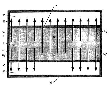
Referring first to the diagrammatic view of Fig. 1A, an electronic circuit
board assembly is shown, as in the before-mentioned standard 19-inch or other
card cage frame or housing G, holding closely positioned pluralities, for
example,
of similar electronic z/o (or memory) boards C~, C2, etc. containing high
speed
signal circuits and provided with powering terminals; and, in the illustrative
and
preferred application of the present invention, requiring high speed switching
amongst the z/o terminals of the boards as, for example, for the type of
internally cached multiple DRAM switching systems described in Mukesh Chatter
U.S. Patent No. 5,799,209, issued August 25, 1998, and the corresponding
foreign counterpart of which appears in PCT publication-W097124725.
Front-to-rear mounting slots or channels M, shown in Figs. 1 B and 1 C as
extending transversely within the frame, receive the boards in vertical
parallel
stacks--an upper set of similar spaced groups C~ and C2 of closely spaced
boards
in an upper section of the frame (mounted in the left quadrant and in the
right
quadrant, respectively}, and with an intermediate central column space S
provided between the groups C~ and C2. Powering terminals E are shown
aligned near the upper edges of the boards C~ and C2, and lower edge terminals
T are provided for high-speed switching interfacing connection over the later-
described main backplane F, with central logic boards here shown as a
switching
fabric comprising vertical logic boards D, disposed in the central space S
between the boards C~ and C2..
CA 02350135 2001-05-09
wo oor~oaz~ Prrnsmoma~
s
In the lower preferably symmetrical section of the frame, similar mounting
slots or channels M', Fig. 1 B, hold a lower set of similar vertical spaced
quadrant
groups C~' and C2' of closely spaced boards, with a similar intermediate
central
space S' provided between the groups C~' and C2'. The powering terminals E'
for
these groups of boards, however, are aligned near the lower edges of the lower
set of boards C~' and CZ' and terminals T' for interfacing connection with the
switching fabric are provided near the upper edges of the boards, 180°
oppositely
to the mounting of the upper sets of boards C~ and CZ, and facing the
switching
terminals T of the lower edges of the boards of the upper groups of boards.
This
assembly permits all of the high-speed switching signals to the upper and
lower
groups of z /o memory boards to end up next to each other and right at the
switch fabric boards D (or, in other applications, CPU or other logic} in the
area
between interfacing connector terminals T and T'.
An upper power backing plane P is horizontally mounted to provide board
plug-in power connection and to support the lateral edges of the set of groups
C~,
and C2.of the upper section boards and extends across the upper section of the
frame, Figs. 1 B and 1 C. This is the zone where the relatively heavy currents
are
being circulated (for example, driven by -48 volts at the power terminals E).
A
similar power backing plane P' is symmetrically mounted to support and power
the set of groups C,' and C2' of the lower section boards and also extends
horizontally across the lower section of the frame. These high power
backplanes
P and P', may be constructed, for example, of copper-clad fiberglass (FR4) and
support the high power high current requirements of the operation of the I/~
CA 02350135 2001-05-09
WO 00/30421 PCT/IB99/01781
~)
board system. The main backplane F between the upper and lower backplanes
P and P', however, is where all the high speed interconnect circuits are
routed
through interfacing terminals T and T'. Not only is there high-speed
communication between ~/o boards in the quadrants and the switch fabric
modules in the center, but also between the 1/o boards themselves.
At the opposite end of the spectrum is the requirement for very high speed
logic interconnect channels comprised of very sensitive signals that can be
adversely affected by noise generated by the switching of large currents. The
main backplane F disposed between the power backplane s P and P', contains
no such power supply currents and is accordingly herein referred to as a "no-
power quiescent zone". The parallel closely spaced logic switching boards D
comprising the switching fabric, thus, are centrally mounted in the frame and
extend in the space S, between the groups of boards of the upper and lower
section sets of boards, and with the backplane F extending horizontally
intermediately of the frame between the upper and lower section backpianes P
and P' and isolatively separate therefrom to provide such no-power quiescent
zone for high speed interconnect signals, such as those of the switching
fabric
boards (or, in other applications, CPU or the like). The switch fabric boards
D
are shown occupying the upper space S, and terminating at their terminal
connections at the main backplane F for connection with the interfacing
terminals
T, T' of the sets of boards C~, C~', C2, Cz'. Substantially symmetrical plug-
in
connections are provided from the lower edge switching terminals T of the
upper
section boards C~ and C2 and from the upper edge switching terminals fabric
CA 02350135 2001-05-09
WO OOI30421 PCT/IB99/01781
Ic)
board T' of the lower section boards C~ and C2 to the switching fabric boards
D
along the backplane F.
In practice, for the internally cached DRAM network application above
described, where 12-16 IIO boards may be stacked in the board groups, the
three backplanes P, P' and F are preferably mounted into a metal frame G, as
with precision-drilled location holes which then locate all of these
backplanes
very precisely and make them appear to simulate one continuous physical single
backplane to all the board cards that are plugging in.
The switching fabric boards D connected with the backplane F are shown
positioned for their interfacing terminals to be in line respectively with,
though
between, the interfacing terminals T, T' of the upper and lower section
boards,
remote from the regions of the board power terminals E and E' at backplanes P
and P'. The power terminals E, E' used on the power backplanes P and P' are
sturdy rugged conventional heavy-duty, heavy current power connectors;
whereas the terminals T and T' used to plug into the F backplane, are very
delicate high-density connectors.
The novel construction of the invention permits the cooling in the system
to be provided, all from the bottom to the top of the frame, and all
unidirectionally
vertically. Since no horizontal boards are used, no convection problems are
present, and there are no issues with thermal heat rising off of one board and
heating the successive boards above it. With the cooling air going straight up
through the frame so that all air horsepower is utilized in cooling the
boards, an
optimized relatively small blower system may be used, even in a 19-inch rack.
CA 02350135 2001-05-09
WO 00/30421 PCT/I899/01781
Further to maintain efficient air cooling of the tightty packed board
assembly, and serendipitously to provide trapping of electromagnetic radiation
generated by the high speed switching within the frame from escaping
therefrom,
an open egg-crate type of metal grill lid, is provided over the top exhaust of
the
frame or housing at L and also at the air inlet at L' .'This not only allows
for
optimum unimpeded or low-impedance uniform flow of air in-line from the bottom
through the top along the surfaces of the board cards, but the square or
rectangular or other cell openings of the metal grill L, L' may be dimensioned
relative to the wavelength of the principal electromagnetic radiation
frequencies
generated by the high speed switching, to serve as electromagnetic wave-guide
cut-off attenuators, trapping or attenuating the radiation within the frame.
For
example, with high-speed switching by the boards D in the range of 12 GHz in
frequency(ies), a cross-dimension of square grill wave-guide-like cells, 'h
inch on
the side and'h inch deep, will provide about 23 to 24dB at the 12 GHz cut off
frequency, and on the order of about 27dB at frequencies well below 12 GHz.
Again, with consideration of air cooling of tightly packed boards and also
of simplicity and low cost of card mounting slot or channel construction, the
mounting slots or channels M, M' may preferably be formed of inexpensive
substantially U-shaped structures as shown in Fig. 2. A metal sheet is there
shown folded, with the upper portion 1 of one side (right) serving as one wall
of
the U-shaped channel, juxtaposed against the lower portion 2 of the other side
(left) of the folded sheet. The other side 2 is then bent transversely at 2'
to form
the bottom of the U channel, along which the board cards are inserted and
CA 02350135 2001-05-09
WO 00/30421 PCT/IB99/01781
12
board cards are inserted and withdrawn, and then the sheet is bent upwardly at
2", parallel to the upper portion 1, to serve as the opposite wall of the U-
shaped
channel. Transverse supports 3 are shown provided between adjacent channels.
While most useful in the illustrative example of the high speed switching
fabric herein described, it is to be understood, as before stated, that the
techniques of the invention are not at all limited to this type of networking
system
or equipment. The architecture of the invention, indeed, is well suited for
computer systems with processor cards (CPUs, before mentioned) located in the
regions illustratively described herein for the switch fabric, and with memory
or
~/o cards disposed in the four quadrants. The centrally located logic boards
may thus be more generically described as switch fabric/CPU cards.
Further modifications will also occur to those skilled in this art, and such
are considered to fall within the spirit and scope of the invention as defined
in the
appended claims.