Note: Descriptions are shown in the official language in which they were submitted.
CA 02350281 2001-06-21
ALARM AND TEST SYSTEM FOR A DIGITAL MAIN LINE
This application is divided from Canadian Patent
Application Serial No. 2,091,067 filed August l, 1991.
BACKGROUND OF THE INVENTION
The present invention relates to the field of
telephone communication. More particularly, in one
embodiment the present invention provides a method and
apparatus for simultaneously transmitting information
from multiple phone connections over a single twisted
pair line.
Techniques for transmission of multiple voice
or data signals over a single phone line are well known
in the telecommunications industry and are commonly
referred to as concentration techniques. In the past,
frequency division multiplexing was the most commonly
used technique for simultaneous transmission of multiple
voice or data signals over a single line. Frequency
multiplexing techniques are still commonly used in, for
example, wideband transmission media.
Digital time division multiplexing techniques
have been used since the 1960's and have become the
most common concentration technique in, for example,
interoffice circuits. An entire family of T-carrier
(Trunk carrier) systems such as T1, T1C, T1D, T2, and
T4, have been developed for concentration of multiple
voice and data signals over a common line. Digital
concentration techniques are described in, for example,
Bellamy, Dicital Teleohony, Wiley and Sons, 1982, which
is incorporated herein by reference for all purposes.
Digital communication has become relatively
standard in, for example, intraoffice trunks. One
example of a method for transmitting multiple voice or
data signals over a single two- or four-wire transmission
line is disclosed in Kaiser et al., "Digital Two Wire
Local Connection Providing Office Subscribers With
Speech, Data, and New Teleinformation Services," ISSLS,
March 20-24 (1978). In Kaiser et al., telephone data,
CA 02350281 2001-06-21
WC . ~ 04794 PCT/hS91 /0~
2
viewdata, telecopier information and the like are
transmitted in a digital fashion over a two- or four-wire
line to a local exchange. Digital data are transmitted
in data bursts which are later expanded and recovered
using, e.g., time division multiplexing techniques.
A generic example of a 2-to-4 wire converters
or hybrid coupling circuits is shown in Fig. 1. In Fig.
1 system 10 is composed of a 2-wire transmission medium
11, first digital device 12 and second digital device 14.
Each digital device contains a receiver and a transmitter
amplifier, the transmitter and receiver amplifiers being
coupled to transmission medium 11. Receiver amplifier 13
and transmitter amplifier 15 are in device 12 and
transmitter amplifier 19 and receiver amplifier 17 are in
device 14. In this application, the circuit which
couples the transmitter and receiver amplifier to the 2-
wire system will be called a hybrid coupling circuit.
Simultaneous transmission and reception over the hybrid
coupling circuit is generally realized as a 2-to-4-wire
conversion, wherein both a reception amplifier and a
transmission amplifier are coupled to the same pair of
wires.
This arrangement has several inherent problems.
The signal being transmitted is typically fairly strong,
having an amplitude of several volts. The received
signal, after transmission line attenuation, is generally
of a much lower order, frequently about several
millivolts. As a portion of the transmitted signal feeds
back to the receiver amplifier, this high amplitude
transmitted signal can drown out the incoming signal.
Additionally, although the impedance of the transmission
line and the transmitter should be matched to achieve the
highest power transmission over the two wire pair, the
impedance which ~is added to improve the transmission
characteristics also further attenuates the incoming
signal. Finally, incoming noise should be filtered off
CA 02350281 2001-06-21
W:~ X2/04794 PCT/US91/(i;a75
3
the incoming signal to improve reception but the
filtering must not affect the outgoing signal.
These problems are known in the art and
attempts have been made to solve them. One known hybrid
coupling circuit is shown in Fig. 2. In combination with
output transformer T1, resistors RF1 are feed resistors
and are selected so that the impedance of the transmitter
will match that of the load ZL. This permits maximum
transmission power. Assuming that the system is mirrored
at the line labelled "Sym" and ZL is 13511, if T1 has no
impedance, then both RFis will be 67.5f1. VPr~ will be 1/2
Vo"c (the RFis act as a voltage divider circuit) and each
end of the circuit can power the other for maximum
efficiency. Resistors RF2 and impedance ZR serve to
mirror the voltage appearing on the primary coil of
transformer T1, that mirrored voltage being labelled VR~r,
In a preferred embodiment, the RFZS and ZR will be a
multiple of RF1 (herein, 5-15 times RF1) and RDis and Rats
will all be equal and approximately 5-15 times RFZ. A
signal transmitted from Vac results in VR~~ being zero as
a result of the voltage divider created by RD1 and RD2,
The voltage divider between VR~r and VPri.K results in the
inverted output signal and the original output signal
being applied to the receiver amplifier simultaneously.
The two signals cancel each other out resulting in a very
large reduction in output signal feedback to the
receiver. At the same time, incoming signals Vs~~o~a vary
while Vo~c remains at zero. VR~r remains at about zero
volts as long as Vo~t remains at zero volts and VR~~ is
equal to 1/2 V~i~, received through the voltage divider
formed from Rnl s and Rn=s .
In terms of output performance, the output of
the circuit shown in Figure 2 is equal to:
VRec VPriise ~ "D2/ ( "Dl + "D2 ) VPriwe / 2 r dS RD
gv2, 1 '
Although the circuit shown in Fig. 2 largely
eliminates feedback signals into the receiver, it still
CA 02350281 2001-06-21
~'G .04794 PCT/US91/OS
4
attenuates incoming signals by about 1/2, due to the
voltage divider. It is desirable to retain the signal
cancellation properties of the circuit shown in Fig. 2
while also achieving an improved incoming signal.
Despite advances in the multiplexing techniques
a variety of problems remain. For example, some
multiplexing techniques continue to require complex and,
therefore, uneconomical equipment. This equipment is
particularly unsuitable for individual or small office
users. Further, when applied to residential users, small
office users, and the like, some systems require that
the user provide a power source such as a transformer
connection to a 120 v. power source, a battery power
source or the like. Some systems require that the
user replace existing two-wire connections with less
conventional connections and/or are limited in the
distance of twisted pair line over which information may
be transmitted. In spite of certain advances in the
ability to transmit multiple voice and data signals over
single twisted pairs, most local switching units continue
to provide a single analog signal over a single twisted
pair to a typical home or office.
Prior techniques for providing service to home
or office users have also provided limited capability for
detection of failures in the system. Testing equipment
has previously included, for example, the so-called MLT
or 4TEL mechanical line testers and the SLIC 96. While
meeting with some success, prior failure detection
systems have met with certain limitations, particularly
when applied to digital systems over twisted pairs
between telephone company equipment and a subscriber.
For example, some prior systems have been able to detect
that a failure has occurred, but have been unable to
identify the location of the failure. Other systems
have been incompatible With existing telephone company
facilities, or with digital twisted pair systems. Other
equipment has required the installation of a test line
CA 02350281 2001-06-21
«'s, X2/0.1794 PCT/L'S91/~~.. i~
between the central office terminal and a remote terminal
at a customer facility. Still other systems have been
exceedingly complex and/or costly.
Limitations with the mechanical enclosures for
5 telephone equipment at customer facilities have also been
encountered. Some enclosures have provided insufficient
weather protection. Some enclosures have provided only
limited access to frequently used components, have been
excessively complex, utilize expensive components or
fabrication techniques, or combinations of the above.
Problems have also arisen in connection with
test ports for customer telecommunictions equipment such
as remote terminals at customer facilities. It is often
desirable to provide an RJ11 connector of the type well
known to those of skill in the art, or other such
connector, at an external loction at subscriber
facilities such as a junction box leading to a house or a
remote terminal of the type described above. Previously,
such access is provided by installing a female RJ11
socket at such locations which is normally connected to a
male RJ11 plug. The tip and ring wires (among others in
some cases) lead from the female RJ11 socket, and connect
to tip and ring connections in the male RJ11 plug,
thereafter leading into the subscriber facility. When it
is desired to connect test equipment to the RJ11 female
socket, the plug is removed, and another male RJ11 is
inserted into the female socket, thereby providing tip
and ring connections for the test equipment.
Problems have arisen with such arrangements,
however. For example, it is sometimes difficult to
establish and maintain an adequate environmental seal in
a removable male~RJll plug, particularly when wires lead
from the male RJ11 plug. Accordingly, moisture and other
environmental contaminants are allowed to enter such
plugs, sometimes resulting in corrosion and/or failure of
the connection of the tip and ring connections in the
socket/plug combination.
CA 02350281 2001-06-21
6
It is desirable to provide an improved and more
economical method and associated apparatus for multiplexing
multiple phone line connections over a single twisted pair
connection especially for use in providing multiple phone
lines over a single twisted pair into a home or office from
a local telephone exchange. It would further be desirable
to provide a system which provides useful alarm and failure
detection systems which are also compatible with
conventional telephone company service facilities. It is
also desirable to provide an improved protection system for
such equipment, as well as test access to customer
equipment.
SUMMARY OF THE INVENTION
Accordingly, the present invention provides an
enclosure for telecommunications equipment, comprising:
a) a frame (1430), said frame defining a telephone
line region (1404,1406) comprising telephone line
connections; and
b) a sealed components case (1402), said sealed
components case enclosing at least one electronics
component (1422) for processing signals from and to said
telephone line connections;
characterised in that said components case is
attachable to said frame with a socket and plug assembly
(1424,1426), further comprising a gel seal in said socket
and plug assembly.
CA 02350281 2001-06-21
7
The gel sealant preferably has a cone penetration
value of 100 to 350 x 10-lmm and an ultimate elongation of
at least 50%. The gel sealant preferably comprises a
urethane, a silicone, or a styrene-ethylene-butylene
styrene.
CA 02350281 2001-06-21
8
The enclosure includes a modular, sealed case for
electronic components mounted on one or more circuit
boards. The sealed case is preferably downwardly facing and
mounted on a second enclosure. The second enclosure
includes a first, user-accessible section and a second,
restricted-access section. The user-accessible section is
covered by a first door and the restricted access section
is covered by a door having a limited access closure device
such as a protected fastener, lock, one-way screw, or the
like.
CA 02350281 2001-06-21
9
The sealed components case preferably encloses a
circuit board for conversion of digital signals from a
twisted pair to analog signals for use in subscriber
telephone equipment.
A further understanding of the nature and advantages
of the invention may be had with reference to the following
figures and description.
BRIEF DESCRIPTION OF THE FIGURES
Fig. 1 shows a generic 2-to-4 wire transmission
system;
Fig. 2 shows a schematic of a known 2-to-4 wire hybrid
coupling circuit;
Fig. 3 is an overall block diagram of the system;
Fig. 4 is an overall block diagram of a remote
terminal (RT) according to one embodiment of the invention;
Fig. 5 shows a schematic of a 2-to-4 wire hybrid
coupling circuit according to one embodiment of the
invention;
Fig. 6 shows a schematic of the 2-to-4 wire hybrid
coupling circuit according to another embodiment of the
invention;
Fig. 7 is an overall block diagram of a line card (LC)
according to one embodiment of the invention;
CA 02350281 2001-06-21
Wfv ;'04794 PCT/US91/0~
Fig. 8a is a block diagram illustrating
portions of the system used for test and alarm functions
and Fig. 8b illustrates the master architecture in
greater detail;
Fig. 9 illustrates the voltage source current
monitor;
Fig. 10 illustrates the RT emulator in greater
detail;
Fig. 11 illustrates the voice frequency
10 OSC/monitor in greater detail:
Fig. 12 illustrates the LC emulator in greater
detail;
Fig. 13 illustrates the PGTC interface and drop
emulator in greater detail;
Fig. 14 illustrates the alarm status interface
in greater detail;
Figs. 15a to 15m are flow charts illustrating
the LC/RT microprocessor code;
Figs. 16a and 16b are. overall block diagrams
illustrating the master control software architecture;
Figs. 17a to 17o illustrate the master control
operation and software in greater detail;
Fig. 18 is an isometric drawing illustrating
the RT housing in a closed position;
Fig. 19 is an isometric view of the RT housing
with open access doors:
Fig. 20 is a detailed fron view of one
embodiment of the customer and telephone company
equipment compartments;
Fig. 21 is a mechanical illustration of the
test access port at the RT or other subscriber equipment;
and
Figs. 22a and 22b are simplified wiring
diagrams schematically illustrating operation of the test
access port.
CA 02350281 2001-06-21
WU 92/04794 PCT/ US91 /05471
11
DETAILED DESCRIPTION OF THE PREFERRED EMBODIMENTS
CONTENTS
I. Definitions
II. General
III. Data Transmission Hardware
A. RT Hardware
B. 2- to 4-wire Coupling Circuit
C. LC Hardware
D. Shelf Control Hardware
IV. Master Control Hardware
A. General
B. Overall Hardware Description
C. Test Hardware
1. VSCM Board (VI)
2. RT Emulator
3. Voice Frequency/OSC Monitor (VF)
4~ LC Emulator
5. PGTC/Drop Emulator Interface
D. Alarm Hardware
V. Software/Microprocessor Functionality
A . RT/ LC
B. Master
1. Software Architecture
2. Test Software Operation
VI. RT Enclosure
VII. Test Access Port
VIII. Power Management
IX. Conclusion
I. Definitions
Certain terms and abbreviations are intended to
have the following general definitions:
ACO - alarm cutoff
CID - craft interface device
COE - central office equipment
COT - central office terminal
CA 02350281 2001-06-21
WG 04794 PCT/hS91/05
12
COAS - central office alarm system
DAML - digital added main line
DSL - digital subscriber line
E2A (SAC) - Telemetry Standard for Alarms:
status and command
E2A (APR) - Telemetry Standard for Alarms:
alarm processing remote
IECQ - ISDN echo cancellation circuit,
quatenary
ISDN - integrated services digital network
LC - line card
ICC - ISDN communications controller
MC - master controller
MTS - message telephone service (otherwise
known as POTS lines)
OS/NE - Operation System/Network Element
(An X.25 connection to central office equipment for
monitoring and control of master controller)
OSC/OSI - Operating System Interface
PGTC - Pair Gain Test Control
POTS - plain old telephone service
RT - remote terminal
SC - shelf controller
SICOFI - dual channel signalling codec filter
SLIC - subscriber line interface circuits
X.25 - CCITT standard for interface to packet
switched networks
2B1Q - Two Binary, One Quatenary, ANSI standard
ISDN line transmission method for encoding 2 data bits
onto a single 4-level symbol
4B3T - four binary, three ternary line
transmission method
IZ. General
An improved method and apparatus for
transmitting and receiving data over a single twisted
pair wire are disclosed herein. The method and apparatus
CA 02350281 2001-06-21
92/04794 PCT/l.'S91/u~47~
13
will find particular utility and is illustrated herein
as it is applied in the transmission of multiple voice,
data, and alarm signals over existing twisted pair lines
which are used to connect homes, offices, and the like to
local switching facilities, or central offices, but the
invention is not so limited. The invention will find use
in a wide variety of applications where it is desired to
transmit multiple voice and/or data signals over a single
twisted pair including, for example, facsimile, computer
l0 data, alarms, and/or low-speed video signals.
The Digital Added Main Line (DAML) descri~:sd
herein is a pair gain system. Parts of the system are
drawn from and compatible with the Bellcore Universal
Digital Channel. The system provides two Message
Telephone Services (MTS) (a/k/a POTS lines), and two
Auxiliary lines over a single copper twisted pair.
The system uses ISDN 2B1Q line format to transport the
signal, is line powered, and includes various self-test
capabilities. The ISDN 2B1Q line format supports two 64
2o kbps voice channels and a single 16 kbps data channel, as
well as additional signalling overhead over a single
twisted pair. The data channel is partially used for
system overhead functions and to support maintenance and
alarm capabilities of the system.
As shown in Fig. 3, the system includes a
digital subscriber line (DSL) 100, connected at the
subscriber end to a Remote Terminal (RT) 102, and at the
central office end 112 to a Line Card (LC) 104. Each
RT-LC pair and it's associated DSL constitute a line
set (IS).
The remote terminal supports the connection
of up to two analog POTS lines 106a and 106b connected
to subscriber equipment 108, and two auxiliary lines
107a, 107b for continuity lines (used in, for example,
burglar alarms). Each of several line cards 104 are
connected to the exchange 109 in the central office by
CA 02350281 2001-06-21
WG .'04794 PCT/US91/OS
14
two analog subscriber lines 110a, 110b. Each line card
also has two additional auxiliary ports 113a, 113b.
Up to, for example, 17 line cards are plugged
into a powered backplane containing a single Shelf
Controller (SC) 114. The shelf controller communicates
with the line cards via a single serial line through a
backplane with a 4.8 kbps asynchronous RS-232, also
referred to as the shelf bus (SB) 116. The shelf
controller serves to monitor and communicate with the
line cards.
Up to, for example, 30 shelf controllers
communicate with one master controller (MC) 118, over an
RS-485, synchronous serial line running at, for example,
48 kbps, also referred to as the frame bus 120. The
purpose of the master controller is to allow local or
remote control and alarm and test functions for the line
sets. The master controller can be controlled from a
front panel 411 or a central office interface (OS/NE)
414, via an X.25 connection. The master controller also
has an additional synchronous serial port RS-232 known as
the craft interface 413 for maintenance purposes and has
various central office alarms 416.
III. Data Transmission Hardware
A. RT Hardware
Fig. 4 is a block diagram of a remote terminal
(RT) 102 according to one embodiment of the invention.
The RT would be placed in, for example, a home, office
or other subscriber facility for transmission and/or
reception of voice or data signals over the single
twisted pair line 100. A plurality of phones or other
subscriber equipment would utilize analog signals
produced by the RT and provide analog signals to the
RT for transmission over the twisted pair.
A conventional two-wire DSL 100, which may be
the type commonly leading into households, offices, or
the like provides input/output to the RT. As will be
CA 02350281 2001-06-21
O 92/04794 PCT/ 1.'S9 i i 05475
readily apparent to those of skill in the art, the
signals transmitted over the DSL could either be a
telephonic voice or data signal from the LC. The
invention will be illustrated herein as it applies to
5 the RT primarily with regard to an incoming signal,
but the process is similarly applied in reverse to
provide voice and data signals from the RT to the LC.
The DSL signal, representing in digital form
a voice or data signal, enters a two-wire to four-wire
to line transformer 202 for isolation and for impedance
matching via a maintenance termination unit 406. The
voice or data signal entering the line transformer 202
is an 80 ksymbols/sec (i.e., kbaud/sec) signal having
one of four voltage levels (2H1Q). While the invention
15 is illustrated herein with regard to the preferred
80 ksymbols/sec signal, it is believed that the invention
herein would find utility using signals of between
about 50 and 100, and preferably between 70 and 90
ksymbols/sec. Using other standards, such as 4H3T
(a ternary symbol), other rates may be desirable such
as 120 ksymbols/sec. The data rates and standards and
rates used herein are of course only illustrative and
will of course vary from one system to the next and
as the underlying technologies evolve. The use of an
80 ksymbols/sec 2H1Q ANSI line protocol signal permits
the transmission and reception of voice and data signals
over extended lengths of twisted pair wires, e.g., 1,000,
15,000, 20,000, 60,000 feet or more, without substantial
smearing, i.e., signal quality over large distances is
improved because the lower frequency 80 ksymbols/sec
signal may be more readily separated. These results are
achieved over conventional line sizes such as 19, 22, 24
or 26 awg.
The signal from the line 2w/4w transformer 202
enters an ISDN Echo Cancellation-Quaternary (IECQ) chip
204 via line 203. The 80 ksymbols/sec 2H1Q ANSI line
protocol signal contains 160 kbits/sec of information and
CA 02350281 2001-06-21
w0 9. .794 PCT/US91/054~
16
the IECQ chip 204 converts the 80 ksymbols/sec signal
into a 160 kbits/sec binary signal. The 160 kbits
includes 16 kbits of control information and 144 kbits of
user data. The ICC operates on a clock signal (CLK) at,
for example, about 520 k~iz and a frame control signal
(FSC) at, for example, about 8 kHz.
Over a one-wire serial bus 213, the ICC chip
206 sends 8 bits of data on one channel, 8 bits of data
on the other channel, 8 bits of control, and 8 bits of
signal data to Codec Filter (SICOFI) 210, and then
repeats, permitting substantially simultaneous
transmission/reception of two or more voice or data
signals. Monitor data, ring data, and other data which
the microprocessor polls are also made available to the
microprocessor.
SICOFI 210 converts the binary bits for each
channel into analog voice or data signals in which
frequency and amplitude are modulated. The analog
signals are then transmitted over lines 209 to Subscriber
Line Interface Circuits (SLIC's) 212a and 212b. SLIC's
212a and 212b are four-wire to two-wire converters and
control the power available for utilization by the
subscriber's phone or other communication device by
superimposing the analog AC signal on DC such as 48 or
24 v. DC. Conventional analog information is provided
to subscriber phones from the SLIC's over lines 214a and
214b.
Ring generator 216 is connected to a line via
relays when it is desired for a phone to ring, under the
direction of the microprocessor. The ring generator is
not active under normal states, and is activated and
connected to the'line via a relay only when a ring signal
is transmitted (in digital form) over the twisted pair in
preferred embodiments. Power supply 218, using a process
more fully described below, provides general power and
ring power to the phones at appropriate times via a ring
bus 220. Test loads 428/430 are used for imposing loads
CA 02350281 2001-06-21
J 92/04794 PCT/US9 ~. J547
17
selectively on the lines under the direction of the
microprocessor during testing operations. Auxiliary
lines 1 and 2 are used for alarms and the like. Relays
selectively connect the ring generator and test loads.
A maintenance port 430 and status indicators 403 may
also be provided in some embodiments.
Outgoing signals from the subscriber are
processed in a similar but reverse method from incoming
signals. In particular, analog signals enter SLIC's 212a
and 212b for two-wire to four-wire conversion via lines
215. Signals from SLIC's 212a and 212b enter SICOFI 210
via lines 209 for analog-to-binary 8-bit word conversion.
These 8-bit words are, thereafter, converted in ICC 206
into a binary stream containing 160 kbits/sec of user
information (144 kbits of user data plus 16 kbits of line .
control) for input to IECQ 204 via line 205. IECQ 204
converts the 160 kbits/sec signal to an 80 ksymbols/sec
quaternary signal for transmission to telephone company
equipment over the twisted pair 100.
B. Two- to Four-wire Conversion Circ>;r
Fig. 5 shows a preferred embodiment of the 2-
to 4-wire conversion circuit 202. As compared with the
circuit shown in Fig. 2, 2 additional "wings" or coils
have been added to the primary side of transformer T1 and
the connections of Rnl and RF1 have been somewhat
rearranged: RF, remains coupled to the central "original"
winding and Rnls is now coupled to the ends of the new,
additional coils of T1.
The additional coils and rearranged resistors
can increase the ratio of VRe~,/V~i~ from approximately 0.~
to almost 1, thereby doubling the detected signal
strength of the incoming signal. A range of results is,
of course, possible, depending upon the ratio of VF~~ab.~k
to VPr~, herein called X and the ratio of VR~f to V~i~,
herein called Y.
CA 02350281 2001-06-21
CVO : X4794 PCT/US91 /0~
18
. As in the prior art, RF1 is again set to match
the load impedance ZL so as to provide proper source
impedance. As the value of an RF.1 is 1/2 of ZL two such
resistors are used to balance the system. RF.~ and ZR are
chosen so that the sum of 2RF2 + ZR is between 5 and 10
times the sum of 2RF.1 + ZL. ZR is set so that VR~r will be
1.2 to 1.5 times larger than V~i~. As Y is the ratio
between VRai and Vpri~, Rn2 = Y ~N and ~1 = X ~N, where N is
any appropriate number to prevent loading the system and
l0 provide reasonable impedance to the receiver system. If
only the wing coils were added to the transformer, the
value of RD1 would have to be increased, proportional to
the increased transformer winding ratio, in order to keep
VR~~ equal to zero. If only the increase of VA~f compared
to V~i~ is considered, RD= must be increased by a factor
of Y to keep VR~~ equal to zero.
In the circuit shown in Fig. 5, Vp~edback- X ~Vprime
given that X is the ratio between VFe~aback and Vpri~. Y, as
previously defined, equals VR~f/Vp=iaK~
Initially,
VRec VPeedbaek ~ "D2/ ( ~1 + "D2 )
However, as Rnl in this embodiment is actually
equal to X ~ RDl and RDZ is equal to Y ~ RD ,
2
2 5 VRec = X ' vpr ime ~ y ' RW/ ( ~1 + YRp2 ) .
Simplifying, with F~ =Ro ,
i z
VRec- VPriax X ' y/ ( X+y )
With reference to the operation of the circuit
shown in Fig. 2, wherein VR~~ -- (Vpri~/2) the performance
of the modified system is consequently equivalent to:
VRac = 1(Vpriwe/2) 2X~Y/(X+Y) .
As shown in Fig. 5, the original voltage
cancellation for preventing feedback of the output signal
is still essentially the same as in the prior art - the
negative of the output signal and the normal output
signal are always simultaneously applied to the irput
CA 02350281 2001-06-21
.J92/04794 PCT'/1JS91iU547:
19
amplifier thereby effectively cancelling out the feedback
caused by the transmitted signal.
In a specific embodiment, Vgeedback~Vprime e~als 3
and VR~f~Vpri~ equals 1.5. The signal strength of the
received signals is increased by 6 db as compared with
the strength of received signals in the circuit shown in
Fig. 2.
In the preferred embodiment, ZR comprises a
first resistor of 532 ti coupled in series to a parallel
combination of a .015 of capacitor and a 3k ft resistor.
RFZ equals 210 f1, Rn2 equals 13 k n, Rnl equals 30K ft and
RFl - 38.7f1. Transformer T1 has a winding ratio of 3 to
1.32, with a .0047 ~cF capacitor being coupled across
Other specific component values could be selected
to optimize performance.
As mentioned, many possible variations of
resistor and impedance values could improve or alter the
performance of the apparatus. In the embodiment of Fig.
5, Y is a maxiumum of 2, limiting the ratio of VRe~ to
VPri~ to 2. In Fig. 6, wherein impedance ZR has been
replaced by a transformer with attached impedances, Y can
be arbitrarily large, resulting in an arbitrarily large
ratio of VR~~ to V~,ix .
C. LC Hardware
Fig. 7 is a block diagram of a line card (LC)
104 which would be placed in a local switching unit,
central office, or other telephone company equipment at
the terminus of a twisted pair wire 100 from a home,
office or the like. The function of the LC is similar
to that of the RT, but reversed, i.e., the LC converts
conventional analog signals from local exchange lines
110a and 110b to appropriate digital signals for
transmission over the twisted pair and converts digital
signals from the twisted pair to analog for transmission
over local exchange lines. Of course, the LC is not
generally power constrained (due to its location and lack
CA 02350281 2001-06-21
~'O 9. .794 PCT/US91/0547
of need to provide ring capability) and may function
using a conventional 48-volt power supply. A DSL power
feed 352 is used to power the RT from the local switching
unit.
5 Ring detects 354a and 354b detect an incoming
ring signal from switch lines 350a and 350b from the two
analog switch lines by AC coupling. When a ring is
detected the microprocessor sends an appropriate digital
ring signal in the line control data so as to ring a line
10 at the RT. Test detects 355a and 355b detect a voltage
indicative of a test request from the local phone
company.
Incoming analog signals enter SICOFI 356 from
the switch lines via two-wire to four-wire converters 369
15 and lines 355a where they are converted to digital, 8-bit
words similar to those in the RT described above. SICOFI
356 transmits to the ICC via bus 357. ICC 358 serves a
multiplexing and data handling function similar to that
of the ICC in the RT and transmits 160 kbits/sec of user
20 information (144 kbits of user data plus 16 kbits of line
control) to IECQ 360 via line 359 for conversion to
80 ksyinbols/sec quaternary signals for transmission over
twisted pair 100 via four-wire to two-wire converter 361
preferrably using circuitry disclosed in the above
referenced and incorporated application. The LC
similarly processes incoming digital information from
the RT in a reverse order.
The functionality of the LC is overseen by
a microprocessor 360, similar to the RT. A clock (not
shown) provides timing information for the microprocessor
and the other components in the LC. Bus 366 serves to
provide an office system interface from system alarms.
Status indications 407 are provided via, for example,
lights, alarms, or the like. Test bus 367 operates
relays and provides connections via relays 371, 373,
and 375 to the test lines TEST INPUT, TEST OUTPUT, and
CA 02350281 2001-06-21
J 92/04794 PCT/lJS9 ~ , X547:
21
TEST DSL, the function of which is described in greater
detail below.
Without in any way limiting the scope of the
invention, Tables 1 and 2 provide a list of commercially
available components which are useful in operation of
the RT and LC, respectively, according to the above
embodiments. It will be apparent to those of skill in
the art that the components listed in Tables 1 and 2
are merely representative of those which may be used in
association with the inventions herein and are provided
for the purpose of facilitating assembly of a device
in accordance with one particular embodiment of the
invention. A wide variety of components readily known to
those of skill in the art could readily be substituted or
functionality could be combined or separated. It should
be noted that CMOS-based devices are preferred (e.g., the
microprocessor) so as to reduce power consumption of the
RT in particular.
ab a
RT Components
Line Transformer 2 13 mh, 1:1.32
IECQ 4 Siemens 2091
ICC 6 Siemens 2070
Microprocessor 8 Intel 80C49, 80C51 or 87C51
SICOFI 10 Siemens 2260, or 2060
SLIC 12 Erickson PBL 3764, or
Harris equipment
Buffer 22 74HC244
CA 02350281 2001-06-21
WO 9~ .794 PCT/US91 /0547
22
Table 2
LC Components
Ring Detect 54 Siemens PSB 6620
SICOFI 56 Siemens 2260 or 2060
ICC 58 Siemens 2070
IECQ 60 Siemens 2091
Clock 62 74HC4060
Microprocessor 60 Intel 80C51, 87C51 or 80C49
D. Shelf Control Hardware
The shelf control 114 is comprised of a
microprocessor such as those listed in the table
above in conjunction with, e.g., a Siemens 82520 HDLC
communication controller. The SC concentrates data
from the various LC's in accordance with well known
techniques.
IV. Master Control Hardware
A. General
Figs. 8a and 8b illustrate test and alarm
equipment for the digital added main line system in
conjunction with abbreviated versions of the master
control (MC), RT, and LC. Test and alarm services are
provided to both the central office line card 104 and the
remote terminal 102 by master test and alarm system 118.
The system is compatible with metallic line testers such
as the MLT, 4TEL and conventional pair gain test
controllers (PGTC) 408.
The remote terminal 102 has two LEDs 403a and
403b for interfacing with the user/service personnel.
The first indicates whether the link is up and the other
indicates power-on, no link. The LEDs are preferably
only active when the RT's limited access enclosure door
is open. There is also a tamper sensor 405 which is
activated when the limited access enclosure is opined,
CA 02350281 2001-06-21
~ 92/04794 PCT/L'S91. ~~475
23
providing an indication to the MC that the device has
been tampered with. A maintenance port 430 may
optionally be provided on the RT for testing by service
personnel from the subscriber facilities.
The line card has a single button on the front
panel for lamp test. The line card 104 has a variety
of LED's 407 to indicate the system states. In one
embodiment they include the following:
- minor: indicates minor alarm condition
- DSL: lit if DSL is connected and active
- test: used to indicate test request received
and under test
- tamper: used to indicate that tamper signal
received from RT
- lines: used to indicate status on line 1
- line2: used to indicate status of line 2
- auxl: used to indicate status of auxiliary 1
- aux2: used to indicate status of auxiliary 2
The shelf controller has two buttons for input
by a user, i.e., alarm cutoff (used to silence alarm);
and lamp test (used to test lamps). Depressing both
buttons simultaneously clears any outstanding alarms.
The shelf controller has four LEDs 409 to indicate the
system status. They include:
- major: indicates, for example, 13 or more
LCs reporting faults
- minor: indicates, for example, 1-12 LCs
reporting faults
- test: indicates that shelf is connected to
test bus
- test OK: 0 LCs are down
The master controller has two user interfaces:
the front panel 411 and the craft interface 413. The
front panel 411 of the master controller allows the
operator to:
- Set a channel into test
CA 02350281 2001-06-21
w'0 92. .. .794 PCT/L.'S91 /0547~
24
- Query status of a channel, including test
status, block error counts
- Silence alarms
The front panel includes an alphanumeric
display element and a keypad 415, with keys for 0-9, up
cursor, down cursor, left cursor, right cursor, alarm
cutoff, test, status, special function, enter, and escape
(level up).
The craft interface 413 includes a DB-25,
RS-232 connection which allows the system operator to
perform operations by connecting either an asynchronous
terminal or a computer. Specifically, from this
interface, the operator is able to perform the following:
- Set a channel into test
- Query status of a channel, including test
status
- Silence alanas
In general, the test and alarm system tests
the functionality of the entire system as well as various
2o subsets of the entire system and alerts a user or
craftsman of any problems. This enables detection of not
only a failure in the digital added main line, but also
definition of the source of the failure. Definition of
the location of any failure enables the dispatch of a
craftsman specific to the problem at hand. For example,
if the problem is in the twisted pair between the COT
and the RT, a line repairman may be dispatched, while a
craftsman skilled in the repair of electronic components
may be dispatched if the problem is located in the COT
or the RT.
B. Overall Hardware Description
The DAML Master Control monitors and controls
all other DAML subsystems including SC and LC subsystems.
By polling all active SC's, abnormal conditions can be
detected by the MC and reported to a Central Office Alarm
System (COAS). In addition to monitoring functions, PGTC
CA 02350281 2001-06-21
wV 92/04794 PCT/US91iU547S
and MLT test requests are detected and test procedures
are initiated by the MC on the selected subscriber line.
The tests are performed by the MC test and a DAML
flexible test bus (DAML FT bus). A Remote Maintenance
5 Terminal (RMT) can, in preferred embodiments, be
connected to any Remote Terminal end module for the
purpose of performing maintenance. A limited number
of simultaneously active remote maintenance terminals
(RMT's) can communicate from the RT via the SC to the
10 MC and access pertinent information about the LC.
The test and alarm hardware is illustrated
in conjunction with the LC 104, the RT 102, and master
control 118 in Fig. 8a. In the particular embodiment
in Fig. 8a, the RT is provided with a maintenance
15 termination unit (MTU) 406 between the twisted pair 100
and the link interface 202. MTU 406 may be, for example,
two voltage-sensitive switches which close when the
voltage reaches a given level (manufactured by, for
example, Tycor). Within the RT 102, RT test termination
20 equipment 412 is provided, including, for example,
absorbent and reflective loads. Data concentrator/shelf
control 114 is provided for management of message
transmission.
The functions of the various pieces of
25 test equipment are carried out under the control
of one or more test microprocessors 402. The test
microprocessors) communicate with phone company
operating system interface via OSS (Operating Support
System Interface) line 414. Line 414 may, for example,
provide an indication of a failure of a channel to the
telephone company directly.
Test mlcroprocessor(s) 402 also provide output
to alarm/alarm relay 416 for a physical indication of a
failure (or non-failure) of any particular component or
components. Alarm 416 may, for example, be appropriately
illuminated lights such as described above, audible
signals, physical connections to phone company facilities
CA 02350281 2001-06-21
WO 91, "4794 PCT/US91/0547:.
26
or, in preferred embodiments, interactive operator
facilities. Microprocessors) 402 also controls the
operation of voltage source current monitor 418 (the VI
board), RT emulator 420, voice frequency OSC (oscillator/
monitor) 422 (the VF board), central office terminal LC
(COTLC) emulator 424, and PGTC interface 426. A digital-
to-analog converter (DAC) 427 serves to convert various
analog signals to digital (and the reverse) to service
microprocessors) 402, voltage source current monitor 418
and VF board 422.
Three test lines are connectable via the SC to
various portions of the MC. They are test input (IN),
test output (OUT), and test DSL (DSL). The VI board is
connectable to all three, while the RT emulator is
connectable to OUT and IN, the VF board is connectable to
IN, the LC emulator is connectable to DSL, and the PGTC
interface is connectable to all three.
Fig. 8b illustrates aspects of the MC in
greater detail. The MC, in one embodiment, is mounted in
a rack-mount chassis with an industry standard STD-Hus.
According to one specific implementation of the
invention, each MC chassis contains the following
STD board components:
- a ZT8809 V20 board 436
- a ZT8830 8088 board 438 with Zendex ZBX 354
Communication unit
- an RS485 Driver PCB 439
- a VersaLogic VL-1225 Analog/Digital
Conversion PCB 441
- a VI Test PCB 418
- a VF Test PCB 422
- an LC Emulator PCB 424
- an RT Emulator PCB 420
- a Central Office Alarm Interface PCB 416
- a PGTC Interface PCB 426
As shown in Fig. 8b, the MC, in one embodiment,
utilizes two Central Processing Units (CPU) located in
CA 02350281 2001-06-21
H'O 92/04794 PCT/C.'S91/05475
27
each of two the boards 436 and 438. Board 436 in one
embodiment is a single board computer based on the
Intel 8088 CPU and modeled against the IBM PC/XT. Its
peripheral devices are mapped according to the IBM PC I/O
map except for two additional timer/counters (Timer 1 and
Timer 2). The actual CPU on board, in one embodiment is
an NEC V20 or Intel 8088 operating at e.g., 8 MHz. Its
maximum on-board memory is 512 kbytes of combined ROM and
RAM. Board 436 is configured as a master processor in
the STD-Bus. The STD-Hus allows for a multi-processor
environment with one master and many slave processors.
Of course, the particular devices discussed above are
merely illustrative of those which could be utilized in
conjunction with the invention and strike a balance
of cost and operating performance. Naturally a wide
array of more or less sophisticated devices could be
utilized without departing from the scope of the
invention herein.
Board 438 is an Intelligent I/0 Control
Processor based on the Intel 8088. Board 438 is
configured as a slave processor sharing the STD-Bus
with board 436. It contains the 8088 CPU operating at,
for example, 8 MHz, memory capacity of 32-kbit ROM and
32-kbit RAM, and a MULTIMODULE ZBX adapter. In one
embodiment, this SBX adapter is furnished with a
Zendex communication module based on the Zilog 8530
communication controller 439 which offers the HDLC
synchronous formats.
In the MC, board 436, hereafter referred to
as the MC Application Processor, is used to handle all
application tasks such as status monitoring, alarm
handling, test request handling, and LC coefficient
supervision. In addition, it handles low throughput
RS232C communications to the MC Front Panel and the
Craft terminal. Board 438, hereafter referred to as
the MC Communications Processor, is used to handle the
CA 02350281 2001-06-21
WO : 4794 PCT/US91 /054
28
communication requirements of the Frame communication
(MC to SC), the OS/NE, and the E2A.
The RS485 Driver PCB 441 is used in conjunction
with the Communications Processor 438 to provide RS485
drive interface.
C. Test Hardware
The major boards of the MC are discussed in
greater detail below, along with a brief description of
their functionality.
1. VSCM Board fVIl
In general, the purpose of the voltage source
current monitor 418 is to detect failures in the twisted
pair between the LC and the RT. In addition, the VSCM
generates ring voltages to test the ring detector in the
LC and generates test voltages to perform checks of the
test detect module in the LC.
Generally, the DSL is tested for shorts between
lines and to ground by disconnecting the DSL from the LC
and connecting the DSL to the VSCM board via the Test DSL
line of a test bus. The system then applies various
voltages to the DSL and checks for shorts between tip and
ring conductors (the two wires of the DSL) and between
either of the conductors and ground.
Fig. 9 illustrates the VSCM board in greater
detail. The board is selected by applying an appropriate
address to the STD bus 502 and detected in address
decoder 504. When the VSCM board is selected, data latch
506 pulls needed data off the STD bus according to means
well known to those of skill in the art.
According to the data on the bus the board
drives appropriate relays with relay drivers 508 for
application of a selected voltage to a selected line.
Relay Kl applies the selected voltage to the line labeled
Test DSL in Fig. 8a (DSL), relay K3 applies the selected
voltage to the line labeled Test Out (Out) in Fig. 8a,
CA 02350281 2001-06-21
w0 92/04794 PCT/US91i05475
29
and relay K3 applies the selected voltage to the line
labeled Test In (In) in Fig. 8a. ,
Using relay K5, the VSCM board can apply a
voltage to the tip wire. The applied voltage may be
selected from either of a constant voltage from a DAC 427
or a 20 Hz signal 510 from the VF board. The selected
voltage is amplified in amplifier 512 having a gain of,
for example, 30.
Current monitor 514 and voltage monitor 516
monitor the response of the system when these voltages
are applied, reporting an analog signal to the DAC for
ultimate determination of whether, for example, a short
is present in the DSL to ground or between the two wires
of the DSL.
As shown in the bottom portion of Fig. 9, a
duplicate set of devices is provided for the ring wire
of the DSL, operated under the direction of relay K4.
2. RT Emulator
As shown in Fig. 8a, the RT emulator 420 is
used to generate signals similar to that which would be
produced by the RT. The RT emulator is used for testing
of the LC, for testing of the LC emulator, and the like,
using signals from the voice frequency board. During
testing, a test signal is injected by the VF board to
the LC while the RT emulator is commanded to connect
absorbent and reflective loads. The resultant reflected
signals from the line under test are then evaluated to
identify any failures in operation of the LC.
3o Fig. 10 illustrates the RT emulator in greater
detail. As with the VSCM board, the RT emulator is
selected by applying an appropriate address to the STD
bus 502. The card is addressed via address decoder 602.
The address for a desired register in the ICC 612 is then
decoded and stored in buffer 604. Data from the STD bus
are held in buffer 606 for the ICC 612.
CA 02350281 2001-06-21
w0 9Z 194 PCT/US91/0547:
Based on data provided from the bus, one of
relays K1 or K2 is closed with relay driver 606 to apply
or receive data from the Test DSL or Test Output lines.
The emulator functions similarly to the RT except that it
5 operates under the direction of the test microprocessor
rather than a dedicated microprocessor. DSL signals
are input to the system via hybrid (two- to 4-wire
conversion) circuit 608 such as the one described in
connection with the above incorporated patent
10 application. These signals are then converted from 2B1Q
to binary in IECQ 610, after which ICC 612 provides
serial data to SICOFI/SLIC 614. These signals are then
subjected to loads 616 and the signals are then reversed
through the system for transmission back to, for example,
15 an LC in test. Alternatively, if the ring generation of
the LC is to be tested, a ring voltage is applied to the
LC and, if the LC is functioning properly, a digital ring
signal is received by the RT emulator, decoded, and the
information transmitted back to the MC for confirmation
20 of correct operation. MTU 618 acts in an analogous
manner to the MTU of the RT.
By enabling selection of connecting the RT to
either the Test DSL or Test Output lines, it is possible
for the test system to perform a self test. Self test of
25 the MC is accomplished by connecting the RT emulator to
the Test DSL line while the LC emulator is similarly
connected. Accordingly, tests of the test system may be
performed in the same manner as tests of the actual LC
and RT.
30 The RT emulator requires no separate power
supply such as with the actual RT since it is located
at the C0. The RT offers a load equivalent to the real
RT with load circuit 616. Preferably, load 616 offers
selection between one of several loads such as 5 and
33 mA to simulate real loads in the RT power supply for
testing of the power feed and/or current limiters in the
CA 02350281 2001-06-21
vr0 92/04794 PCT/L:~S91~05475
31
LC. In the RT emulator absorbent and reflective loads
may be emulated by the SICOFI under control of the MC.
3. Voice Frewency/OSC Monitor (VF)
As shown in Fig. 8a, the voice frequency
OSC/monitor 422 produces, for example, a simulated
voice signal which is transmitted to the RT. From an
evaluation of the amount of the reflected signal returned
to the LC by absorbent loads 428 and reflective loads
l0 431 in the RT it is possible to determine the overall
function of the system. Hy "absorbent load" it is
intended to mean herein, for example, a 600 ohm load.
By reflective load it is intended to mean, for example, a
short curcuit. Fig. 11 illustrates the voice frequency
OSC/monitor in greater detail.
As with the other boards in the MC, the address
decoder 702 and the data buffer 704 of the VF board are
connected to the STD bus 502. Depending upon the data
obtained from the bus, the board operates relays K1, K2,
and K3 via latches and drivers 708.
Function generator 710 is a waveform generator
capable of generating a constant 20 Hz signal or
generating a sweeping signal which alternates between
various frequencies typically encountered in voice
transmission. The specific output of the function
generator is selected by way of relay K3. When the 20 Hz
output is selected, it is passed through driver 712 and,
thereafter, to the test input line for the ring test
function of the MC. When the sweep function is selected,
the signal passes through driver 714, transformer 716,
and, thereafter, to either the Test Input line or the LC
Emulator, depending upon the selection of either the K1
or K2 relays.
Loop current detector 718 is used for detection
of loop current and is used to detect a condition in
which the LC has seized because the phone is off the
hook. For evaluation of returned signals, the reflected
CA 02350281 2001-06-21
WO 9:. .794 PCT/LJS91/0547.
32
voltage is passed through a filter 720, RMS converter 722
and, thereafter, to the DAC on the MC.
4. LC Emulator
As shown in Fig. 8a, the LC emulator 424
produces a test signal or signals which emulate the
actual LC from the voice frequency OSC/monitor 422,
and transmits the signal to the actual RT or RT emulator.
At least one of these test signals is in the voice
l0 frequency bandwidth. The system then measures the
reflective signals at various terminations for a
determination of whether the RT is functioning properly.
Fig. 12 illustrates the LC emulator in greater detail.
As with the other boards, address and data are
read from the STD bus. The address is decoded in decoder
802 and data and address information are latched into
address buffer 804 and data buffer 806. Based on data
input to the data buffer, relay driver 808 operates
relays K1 and K2. When relays Kl are engaged the LC
emulator is connected to the DSL. Relay K2 connects
the LC emulator to the voice frequency board. When
connected, input from, for example, the VF board is input
to transformer T1, processed through hybrid circuit 810
for two-wire to four-wire conversion, and thereafter is
processed through SLIC 812, ICC 814, IECQ 816, and hybrid
circuit 818 and transformer T2 for output to the DSL in
a manner analogous to the LC described above, using the
improved two wire to four wire conversion described in
the above incorporated patent. DSL power feed 820
supplies the RT with power in a similar fashion as the
actual LC during testing operations. Necessary clock
signals are generated by XTAL OSC 824 and frequency
divider 822.
5. ~GTC/Droo Emulator Interface
As shown in Fig. 8a, the emulator 432 serves to
convert the various digital signals obtained from the
CA 02350281 2001-06-21
WO 92/04794 PCT/1JS91/05475
33
various tests in the system to voltage signals compatible
with conventional pair gain test controller 408. PGTC
interface 426 serves as an interface between the 28-wire
PGTC 408 and the digital test system 118. Conventional
pair gain test controllers and their interfaces are
disclosed in, for example, "Interface Between Loop
Carrier Systems and Loop Testing Systems," Bell. Comm.
Res. Tech. Ref. TR-TSY-000465 (Issue 2, April 1987) which
is incorporated herein by reference for all purposes.
Fig. 13 illustrates the PGTC interface 426 and the drop
emulator 432 herein in greater detail.
The PGTC is connected to the standard bus
and inputs an address-to-address decoder 902 and data
decoder 904, respectively. The data input to the data
transceiver are transmitted to PIA 906 such as a model
no. 8255 made by Intel. PIA 8255 drives relay drivers
910 and 912 which control the interface with relays.
The optical isolators 914 and 916 are for connecting/
disconnecting loads. Responses are built into the line
set code if, e.g., a reflective load must be connected
when a ring is detected. The load portion 920 of the
device serves as a dummy load in view of the so-called
"golden pair" wire which is used in conventional MLT
systems.
If the MLT system detects a pair gain circuit
"signature," the system will apply a positive voltage
to the tip conductor of the DSL with the ring conductor
open. When this condition is detected the line card will
apply a 333.3 Hz tone between tip and ring towards the
PGTC. In the line card hardware this tone is generated
by the SICOFI under control from the CPU and the CPU
sends an appropriate message to the MC. The PGTC then
waits for acknowledgement from the master control which
will. ground the SEIZE lead with the appropriate relay.
When this SEIZE signal is present together with the
333.3 Hz tone, the PGTC will return a PROCEED signal to
the master control. The conventional PGTC system has
CA 02350281 2001-06-21
WOS 4794 PCT/L'S91/054i_
34
four test pairs, designated 1 through 4 in Fig. 13. Upon
receipt of the PROCEED signal on one of the leads PROCEED
1 thru 4, the master control will close the relays of the
tip and ring conductor 1, 2, 3 or 4, depending on the
test channel indicated by the PROCEED lead.
There are two exception conditions which will
prevent the PGTC test from proceeding. They are a) when
the MC is a major alarm state it will ground the TMAJ
lead and the PGTC system will remove the test request
signal: and b) when the test bus is already in use,
i.e., one of the four pairs is used, and a test request
for another line is received, the SEZBY lead will be
grounded. With a standard carrier system this signal is
used to indicate that the "golden pair" is already in
use.
Two options are available upon receipt of the
PROCEED signal:
1) The tip and ring of the test pair are
connected to one of the terminations 920 and the drop
emulators and the PGTC system performs a channel test; or
2) The tip and ring of the DC test pair are
connected to the DSL and the line card is connected to
the RT emulator. The test system can do a metallic test
of the real pair and the PGTC does a channel test of the
line card connected to the RT emulator. In this case the
MC connects the DC test pair to the DSL by closing the
appropriate relay and connects the line card to the RT
emulator by disconnecting the line card from the DSL and
connecting the RT emulator to the TEST OUTPUT line.
When these connections are made the MC will
ground the appropriate SLEEVE lead to signal that the
necessary connections are made. Upon receipt of the
SLEEVE signal the PGTC sends a LOCK signal and removes
the PROCEED signal to the carrier system, indicating that
all connections have been completed. When the loop
testing system removes the positive voltage from the tip
of the test trunk the PGTC completes the connection of
CA 02350281 2001-06-21
v. v 92/04794 PCT/ L,'S91 i u5475
the test trunk from the MC to the DC test pair (otherwise
referred to as a "golden pair"). Removal of the LOCK
signal indicates to the MC that testing has been
completed and that all test connections are to be
restored to normal. If a second test request is received
for the same line, the "other" procedure is applied.
Note the INHIBIT lead is not used in a DAML system as
there is no real test pair or golden pair.
When an MLT test is detected by the LC, the MC
10 will connect to the test pair of the MLT system. There
are then two options:
1) The MLT system gets a resistive termination
from which it can derive the status of the line: OK,
LC fault, RT fault or DSL fault. In case of a DSL fault,
15 access is given to the pair: or
2) The MLT system can get immediate access to
the pair.
Either of these options can be chosen as
default. When a second test request for the same line
20 is received the other option will execute.
The PGTC interface allows a full testing by the
Maintenance Center: the PGTC can do the channel test and
the MLT or equivalent can do a test of the twisted pair.
The system offers appropriate resistive signatures to
25 indicate where the problem is based on the results of the
test.
D. Alarm Hardware
Fig. 14 illustrates the alana status board 416
30 in greater detail. An address decoder and data
transceiver input address and data information from the
STD bus via decoder 1002 and data transceiver 1004,
respectively. Data are input to PIA 1006 such as a model
no. 8255 made by Intel. PIA 1006 also receives input
35 from optical isolators 1008. Optical isolators 1008
interface for input with four signals, i.e., CO Alarm
Cutoff, which is a signal which shuts off the alarms at
CA 02350281 2001-06-21
WO 9. .794 PCT/US91/0547_
36
the direction of an operator, PSF, which is a power
system fault alarm from each power supply, and 1,2 E2ASAC
which are relay-activated telemetry systems. The output
of PIA 1006 activates relay drivers 1010, which
' selectively drive 12 relays for activation of lights,
buzzers, or the like, or for activation of the telephone
company alarm system. In one embodiment, 8 alarms are
output to the telephone company, as shown in a typical
relay 1012 and 4 alarms are output at the CO, as shown
with a typical relay 1014.
V. S~,~,tware/Microprocessor Functionality
A . RT,/ LC
Operational software for the RT microprocessor
208 has been developed for use with, e.g., an Intel 80C51
microprocessor, although it will be apparent that the
invention could be applied to a wide variety of such
processors. Operational software has been developed for
use in the microprocessor 360 in the line card. This
code has been used in the Intel 80C51. Again, however, a
wide variety of microprocessors could be used herein
without departing from the scope of the invention.
Figs. 15a to 15m illustrate overall operation
of the LC and RT software. In particular Fig. 15a
illustrates overall operation and architecture of the LC
software. The software includes a main section 1101, an
interrupt service routine for the ICC 1102, an interrupt
service routing for clocks 1103, and an interrupt service
routing for handling serial data 1104.
In the main section 1101 the system first
initializes the various pieces of hardware and software
at step 1105. The system then begins a main loop 1106
through which the system repeatedly cycles until the
system is disconnected from power. The interrupt service
clock initiates a section of code 1117 which performs
routine operations needed during operation of the LC.
The interrupt service for the ICC 1102 contains a section
CA 02350281 2001-06-21
H'O 92/04794 PCT/l)S91/05475 .
37
of code 1107 which handles DSL needs, and the interrupt
service for serial data 1104 contains a section of code
1108 which handles various serial data requirements.
Fig. 15b illustrates the LC initialization and
main loop 1105 and 1106 in greater detail. The
initialization includes steps of hardware initialization
1109, memory initialization 1110, and timer/interrupt
initialization 1111. The main loop then begins.
At step 1112, the SICOFI coefficients are set
up and since this step occurs in the main loop may be
varied over time. At step 1113 the system processes the
serial port receiver. At step 1114 the system processes
the serial port transmissions, and at step 1115 the
system services watch dog timers. The system then idles
at step 1116 until an interrupt is received.
Fig. 15c illustrates the interrupt service 1117
in greater detail which is initiated based on a clock at,
for example, 160 Hz. At step 1118 the system executes
error control code and at step 1119 retrieves local
status information. The system then services the first
line (line "A") at step 1120 and the second line (line
"8") at step 1121. At step 1122 a section of code
provides output control and at step 1123 alarms are
serviced. At step 1124 the system services the front
panel display and at step 1125 the system provides DSL
power control. At step 1126 the system sends DSL status
information to the RT.
Fig. 15d illustrates the ICC chip service
routine 1107 in greater detail. At step 1126 the system
handles various fault problems and at step 1127 does
synchronous transfer of data. At step 1128 the system
handles various aspects of IECQ control and at step 1129
receives a message from the DSL.
Fig. 15e illustrates the serial interrupt
service routine for the port shelf 1108 in greater
detail. At step 1130 the system determines if a message
is transmitted or received. At step 1131 the system
CA 02350281 2001-06-21
WO 92/. ~4 PCT/ US91 /05475
38
outputs a byte for a buffer or, if a message is to be
received, inputs a byte to a buffer at step 1132.
Fig. 15f illustrates the procedure 1113 used
for receiving data on a serial port in the main loop.
At step 1133 the system determines if a message has been
transmitted and, if not returns to the main loop. If
a message has been received, at step 1134 the system
determines if it is a status request and, if so,
processes the request. If not, at step 1135 the system
determines if the message is a test request and, if so,
processes it. If not, at step 1136 the system determines
if a maintenance message is present and, if so, processes
it. As shown in step 1138 the system may also be
implemented to test for and process other types of
messages.
Fig. 15g illustrates the process 1114 for
transmitting outgoing messages in the main loop. At step
1139 the system determines if a message needs to be sent
and, if not exits back to the main loop. If a message
needs to be transmitted at step 1140 the system sets up
for transmitting the message and at step 1141 tests to
see if a test response is due. If so, the system adds
the data and returns to the main loop. If not, the
system tests at step 1142 to determine if a model
response is due and, if so, adds the data. If not, the
system proceeds to test for other responses due at steps
1143 and 1144 and, thereafter, returns to the main loop.
Fig. 15h illustrates the architecture and
overall operation of the RT program. As with the a
code, the RT code includes a main section 1145, an
interrupt section for the ICC service 1146, an interrupt
section for clock-based routine service 1147, and a
section for handling interrupts for serial data service
for maintenance operations 1148. The main section 1145
initializes the hardware and software at step 1149 and
then recursively iterates through a main code section
1150.
CA 02350281 2001-06-21
WO 92/04794 PCI"/l.'S91 /0547
39
Fig. 15i illustrates the main section of code
1145 of the RT in greater detail. At step 1151 the
various pieces of hardware in the RT are set up and the
various memory locations are set up at step 1152. Timers
and interrupts are started/set at step 1153. Thereafter,
the system enters the main loop. As with the LC, the RT
SICOFI coefficients are set up within the main loop at
step 1154. Maintenance messages are then processed at
step 1155 and a test request (if present) is processed at
step 1156. Watch dog timers are set at step 1157 and the
system then idles until an interrupt is received at step
1158.
Fig. 15j illustrates the clock interrupt
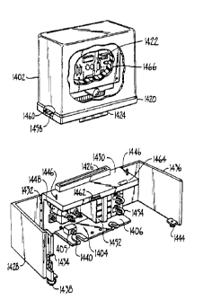
service routine 1147 in greater detail. At step 1159
the system executes an error control sequence and,
thereafter, at step 1160 obtains local status
information. At step 1161 the system services line A
and, thereafter, at step 1162 services line B. The
system then executes an output control sequence at step
1163 and, at step 1164 services various alarms. At step
1165 the system reports service status and at step 1166
the status information is sent over the DSL to the LC.
Fig. 15k illustrates the ICC interrupt service
routine 1146 in greater detail. At step 1167 various set
up steps are conducted and at step 1168 the system does
synchronous transfer of data to, e.g., the SICOFI. At
step 1169 the system determines if additional data are to
be transferred and, if so, returns to step 1168. If not,
the system then handles IECQ control at step 1170 and,
thereafter, receives a DSL message at step 1171. At step
1172 the system then handles any faults.
Fig. 1T1 illustrates the interrupt service
routine for serial port maintenance 1148. At step 1172
the. system determines if it is to transmit or receive.
If it is to transmit, at step 1173 the system outputs a
byte from a buffer. If it is to receive, it inputs a
byte to a receive buffer at step 1174.
CA 02350281 2001-06-21
WO y_, J4794 PCT/US91/054. _
Fig. 15m illustrates the line service routine
used at steps 1161 and 1162 in the RT. At step 1175
the system gets a state pointer and, if there is an
indication to power down, the system does so at step
5 1176. If not, the system determines if an idle state is
desired and, if so enters the idle state at step 1177, or
if not checks for and, if necessary, enters a hold state
at step 1178. At step 1179 the system determines if
there is an on-hook condition and, if so, enters an
10 active state. At step 1180 the system determines if
there is a dial hold state and, if so, does a dial hold.
If the system determines there is an on-hook active
situation at step 1181 the system does an on-hook
routine. If the system determines there is a ring wire
15 condition at step 1182, it performs a ring wire routine,
and, if there is a ring condition, performs a ring
routine at step 1183. At step 1184 the system determines
if a ring stop is to be executed and if so does a ring
stop routine.
B. Master
The MC software is primarily resident with the
Application Processor and operates the various hardware
peripherals which perform the test and alarm functions
herein.
The software is developed in a structured
methodology using top-down design and bottom-up
implementation practices. The code in the MC can be in
the particular example shown herein is programmed in the
~~C~~ high-level language or 8088 Macro-assembly. Of
course, the programming language and microprocessor
environment will'vary widely from one application to
the next.
The software preferably includes application
modules interacting with lower-level hardware drivers
architectured in a structured manner. The glue
logic of all application modules and driver is a
CA 02350281 2001-06-21
Wn 92/04794 PCT/tJS91/0547~
41
priority-based, multi-tasking, real-time, non-preemptive
datagram operating kernel.
A datagram kernel provides the capability
to application modules to be distinctly separated by
function and still be able to intercommunicate and
perform the combined functions of master controller.
Generally speaking, MC application modules activate
other modules by initiation of a datagram.
1. Software Architecture
Fig. 16a illustrates the overall architecture
of the MC software in the Application Processor. At the
top of the MC Application Processor (MCAP) hierarchy is a
MC System Manager module 1201 which oversees the
functions of the MC including status monitoring, alarm
reporting, line testing, coefficient management, and
others. The MC System Manager initiates and manages
subservient modules. The modules are: Command
Interpreter 1203, Poll Handler 1205, Alarm Handler 1207,
Test Supervisor 1209, Coefficient Handler 1211, and the
Self-Test Supervisor 1213. The System Manager 1201, via
a DSOS operating. kernel 1215, provides communications
input/output to front panel driver 1217, craft terminal
interface 1219, OS/NE node driver 1221, and frame bus
driver 1223. The system manager also provides test and
alarm input/output to LC emulator driver 1225, RT
emulator driver 1227, input handler 1229, and output
handler 1231.
The Command Interpreter 1203 provides an
interface to various external portions of the system
and includes a front panel interpreter 1237, a craft
interface interpreter 1239, an OS/NE interface
interpreter 1241, and a maintenance port interpreter
1243.
The Poll Handler 1205 is primarily responsible
for requesting information from the shelf controls. Any
abnormalities detected by the Poll Handler will be
CA 02350281 2001-06-21
WO 9. 794 PCT/L1S91/OS47
42
reported to the pertinent application module. The Alarm
Handler 1207 is responsible for reporting, recording, and
handling of alarm conditions created by LC's or SC's.
The Test Supervisor 1209 is responsible for
supervising the various test modules including the line
set test module 1237, MLT/4TEL test module 1239, and PGTC
test module 1241. Within the line set test module 1237,
the system includes channel test module 1243, DSL test
module 1245, LC test module 1247, and RT test module
1249. The LC test module and RT test module include RT
emulator handler 1251 and LC emulator driver 1253. These
subservient modules, under the general supervision of the
Test Supervisor, interact with the MC test hardware and
DAML test bus to execute the required tests.
The Coefficient Handler 1211 handles the
support to special line coefficients, coefficient
loading, and coefficient reports. The Self-Test
Supervisor 1213 is responsible for performing integrity
tests to the MC hardware subsystem. Tests can be
performed on an on-demand basis, or on a scheduled basis.
Subservient modules to the self-test supervisor include a
CPU board verifier 1255, a power supply verifier 1257,
and a test subsystem verifier 1259. The CPU board
verifier is a normal PC board test. A test of the power
supply is conducted in the power supply verifier.
The MC applications processor (MCAP)
communicates with the MC Communication Processor by means
of a full-duplex mailbox process which operates in the
background and independent of the application tasks.
Datagrams containing SC status information and other
types of messages are passed back and forth between the
MCAP and the Communication Processor using the command
interpreter 1203. At the MCAP end, the messages are
ultimately delivered to the corresponding module. At the
Communication processor end, the destination would be
a communication port such as the Frame Bus to the SC's
or the X.25 connection to the OS/NE. All of the top
CA 02350281 2001-06-21
.. J 92/04794 PCT/US9'1 /U5475
43
level modules have available a number of drivers,
specialized utilities, and general purpose operating
system utilities such as queue handling, and timers to
perform their assigned tasks.
From power-up, the MC System Manager directs
an organized start-up of all other modules depending on
whether the MCAP is starting from a cold start reset or
a warm start. A cold start occurs when the system is
powered-up for the first time from factory parameters.
A warm start occurs if for some unforeseen reason the
system is reset during operation, or as part of a
software error recovery procedure.
During a cold start, the System Manager 1201
instructs the Self-Test Handler 1213 to begin a one-time
test. If all tests pass, the System Manager begins
operation. If any test fails, the System Manager issues
a failure report via the designated system console. If
the failure corresponds to a critical hardware component
such as RAM memory failure, the start-up process is
halted. Otherwise, the system is started in a degraded
mode. The self-test may also be started on a periodic
basis. This periodic self-test can be programmed after
cold start using the system console. The self test is
conducted by connecting the RT emulator and the LC
emulator and performing the normal test sequences in the
test subsystem verifier.
After the one-time self-test is completed, the
System Manager continues the cold start procedure. Part
of this procedure may be prompting the system operator
to enter configuration data via the system console. For
example, PGTC selected test procedure.
During a warm start, the System Manager retains
all its data, and it reports the cause for warm start
to the system console. Finally, after completing the
start-up procedure, regardless of whether cold or warm
start, it activates all subservient modules.
CA 02350281 2001-06-21
WO 4794 PCT/t,~S91/05<
44
After the System Manager activates the Poll
Handler, the LC and SC status information is gathered one
at a time. When the Poll Handler is activated initially,
it polls each SC from numbers 1-30 and gathers
information. From this activity, the Poll Handler is
able to record the status of SC's and LC's that respond
to the poll.
The Poll Handler begins by issuing a STATUS
REQUEST message to each SC starting from SC number 1 to
the maximum number of 30. The STATUS REQUEST messages
are automatically routed via the Communication Processor
and then to the Frame Bus. Those SC's that do not
respond after a predetermined timeout will be considered
inactive or not connected. Those which respond to the
call and send their status information are further
analyzed.
SC's which respond to the STATUS REQUEST are
analyzed to determine the status~of their LC's. The
information for all active LC's and SC's is recorded.
2o If during the process of acquiring SC/LC status abnormal
conditions such as minor alarms are detected, a message
is issued to the Alarm Supervisor. For every LC which
is down, a message DOWN LC REPORT is sent to the Alarm
Supervisor. From time-to-time, other application modules
or even modules which are external to the MCAP (for
example, the RT maintenance terminal) may desire to
request status information about a particular SC or LC.
When the Poll Handler begins polling all SC's,
it does so at a rate of, for example, one SC every
10o msec. This polling cycle, which can be modified
using the system console, is optimal for detecting LC
ring conditions Which are the most rapidly changing of
the LC-related information.
The Alarm Handler 1207 is responsible for
reporting, recording, and handling alarm conditions
created by LC's or SC's. The following conditions are
evaluated for possible alarms:
CA 02350281 2001-06-21
WO 92/04794 PCT/US91/05475
a) LC's are monitored for link down. This is a
minor alarm 1216.
b) SC's are monitored for having from 1 to 11
LC~s down. This is a minor alarm 1214.
5 c) SC's with 12 or more LC's down are
considered major alarms 1218.
d) The system with 1 to 25 LC's down, or up to
a maximum of 11 LC's down in one SC is considered to be
in a minor alarm state. Similarly, 26 or more LC's
10 reported down, or 12 or more LC's on one SC is considered
a major alarm.
The Test Supervisor 1209 is responsible for the
specialized task of testing and servicing the CO test
request. The Test Supervisor has several subservient
15 modules which handle each special test procedure,
including the line set test module, the MLT/4TEL test
module, and the pair gaing test control module. The
specialized test modules are: LC Emulator Handler,
RT Emulator Handler, Line Set Handler, LC Test Handler,
20 and RT Test Handler.
Each test module is given the START TEST
command. Upon test completion, the corresponding modules
respond with a message further qualifying the test
outcome, whether passed or failed, and a test report.
25 The Coefficient Supervisor 1212 handles the
support to special line coefficients, coefficient
loading, and coefficient reports.
When an LC becomes operational, a message will
be sent by the LC to the Coefficient Manager. The
30 Coefficient Manager will verify if there are special
coefficients for the specified LC which may require
loading.
If the newly logged LC is listed as requiring
special coeffcients, a message is sent to the remote LC
35 unit via the corresponding SC. After a predetermined
time, the Coefficient Manager will compare the loaded
coefficients with the one sent. If both transmitted and
CA 02350281 2001-06-21
VVO '~ ' 4794 PCT/l.'S91/054
46
received versions match, the loading is considered
successfull. Otherwise, the process is started again.
The Coefficient Supervisor will retry
coefficient loading several times. If after this time
it is still unsuccessfull, a warning message is sent to
the system console indicating the problem condition.
The Self-Test Handler 1206 is responsible for
performing hardware integrity tests to the MC subsystem.
Tests can be performed on an on-demand basis or on a
regular basis. The IECQ handler and SICOFI handlers
manage operation of the MC SICOFI and IECQ.
The MC Communication Processor (MCCP) software
includes communication link control modules which
transmit/receive data in a format specific to the channel
being serviced. These modules perform the link control
functions in an ISO layered architecture. The link
control modules are: Frame Link module, OS/NE Link
module, E2A Link module, and Mailbox Link module.
Link modules are supported by their respective
communication drivers which are normally Interrupt
Service Routines (ISR). These drivers correspond to
their link control counterpart of the same name: Frame
Driver, OS/NE Driver, E2A Driver, and Mailbox Driver.
The channel formats that will be provided for .
the DAML MCCP are: Frame for the MC-SC Frame bus, X.25
for OS/NE, Serial Asynchronous for E2A, and the Mailbox
format.
A Router module which provides the network
layer functions interfaces with all communication drivers
and is capable of routing message packets from channel to
channel. The routing is dependent on a routing table
which matches destination module name with channel
number. Thereby, messages need only be coded with a
destination and the Router module would identify and
route the message to the proper channel. At the end of
the routed channel where the destination module is
expected to reside.
CA 02350281 2001-06-21
WU 92/04794 PCT/LS91/05475 .
47
2. Test Software ODerati
Fig..l6b is an overall flow chart illustrating
the functionality of the test and alarm system. It will
be recognized that the master provides test capability to
a number of RT/LC users (e. g., 100 or more) and that this
process is rapidly repeated for each of the RT/LC pairs.
The system initially performs a test at step
1202 to determine if a line set is busy and, if not, a
shelf is selected at step 1204. The system then performs
an entire system test or channel test 1206 which tests
the efficacy of the entire system from telephone company
lines to and including the RT equipment. If the test is
O.K. (step 1208), a report is made at step 1210 and the
shelf is deselected at step 1212. If the channel test is
not O.K., an RT emulator is then utilized to perform a
test of the LC at step 1214. The voltage source current
monitor is then utilized at step 1216 to determine if a
failure such as a short between wires or to ground has
occurred in the twisted pair between the master and the
RT. If a failure is detected in the twisted pair,
reports are made at step 1210 such that, for example, a
line repairman may be dispatched to repair the twisted
pair. If the DSL test is passed, a LC emulator is
utilized to test the functionality of the RT at step
1218, followed by status reporting at step 1210.
Fig. 17a is a more detailed flowchart
illustrating the optional line set test 1202. This
portion of the test is skipped if a request to this
effect is made. At step 1302, upon a provisional test
request, the MC will check whether line A or B of the
selected LS is busy. If one of the two lines is busy,
the system increments a counter at step 1304 and, if the
counter is greater than a selected number (step 1306),
returns a line busy message at step 1308. If the counter
is not greater than 10, the system waits a selected time
CA 02350281 2001-06-21
w0 S X794 PCT/ US91 /054'
48
at step 1310 and repeats busy-check. If none of the
lines is busy, the test system continues.
The system then selects the appropriate shelf.
Fig. 17b illustrates the select shelf step 1204 in
greater detail. At step 1312 the system broadcasts a
message to all shelves to disconnect from the test bus.
Then, at step 1314, the system connects the selected
shelf to the test bus by transmitting an appropriate
message to the SC.
The system then performs a channel test; this
checks the performance of both voice channels. In
general, the channel test includes the steps of selecting
the line, issuing a test request, performing an absorbent
test, performing an on-hook test, testing the ringer,
performing a reflective test, and deselecting the line.
Fig. 17c illustrates the channel test 1206 in greater
detail. At step 1316 the system checks whether the DSL
of the selected line set is up (i.e., if the IECQ~s are
linking . If the DSL is not up the system waits for a
short time and trys again for a selected number of times.
If the DSL is still not up, the system logs the status in
the test status database for the specific SC/LC, time
stamps it, and exits the channel test at step 1318. This
procedure is necessary because the Line Set may be trying
to link. Especially when the LC Emulator or RT Emulator
are used, it will take some time before they are linking.
If the DSL link is up, the system continues.
The system then performs a test of line A. The
system initially selects the desired line at step 1320 by
transmitting a message to the selected LC. This also
disconnects the line card from the exchange. A delay of,
for example, 250~ms, may be allowed at step 1322 to allow
for the LC to get the message and for confirmation to
get back to the MC that the line is selected. The
confirmation of the LC is checked and the result is
logged.
CA 02350281 2001-06-21
WO 92/04794 PCT/US91/05475
49
The system then proceeds to test the selected
line. At step 1324, the VSCM board Tip and Ring voltages
are set to 0 volts. A delay of, for example, 15 ms may
be allowed for the lines to settle. At step 1326 the
system connects the VS board 418 to the input of the LC.
A delay of, for example, 25 ms is then allowed for
settling of the relays. At step 1328, the system applies
a test request voltage of, for example, 113 volts to the
tip of the VS board. The ring wire or line is left open.
A delay of, for example, 250 ms is then allowed for
settling of voltages and for the LC relay to get to the
MC. At step 1330, the system checks for an LC test
request message and logs the result. The system then
resets the voltages of the VS board to 0 volts at step
1332. A delay of, for example, 100 ms is allowed for
settling of voltages and the VS board is disconnected
from the LC input.
The system then performs an absorbent test of
the selected line. As shown in Fig. 17d, at step 1334
the selected line of the RT and the absorbent load of the
RT are connected to the RT test bus by transmitting a
message to the LC. This will close the seize relays as
it simulates an off-hook condition and disconnect the
subscriber from the line. At step 1336 the system
selects the frequency sweep on the VF board. At step
1338 the VF board is connected to the test input line.
A delay of, for example, 275 ms is then permitted to
allow for MC to RT transmission, for settling of relays
at the RT, and for RT to MC transmission. At step 1340
the system checks the confirmation of the RT and logs the
result. At step 1342 the system reads the reflected
voltage from the~DAC input, allowing for delay of, for
example, 100 ms for settling of A/D conversion.
_. At step 1344 the system compares the reflected
voltage with a reference values) and, at step 1346,
logs the result. At step 1348 the absorbent load is
disconnected from the RT test bus by transmitting a
CA 02350281 2001-06-21
«'O. X4794 PCT/(.'S91/054
message to the LC. This creates the on-hook condition.
The seize relays will open as the RT will see on-hook.
Fig. 17e illustrates the on-hook portion of the
channel test. The VF board is still connected to the
5 test input line and the line at the RT is connected to
the open RT test bus. After a delay of, for example,
275 ms to allow for MC to LC delay plus relay delay,
LC to MC delay, and RT to MC transmission, at step 1350
the system checks for confirmation of the absorbent
l0 disconnect from the RT. The system then reads the
reflected voltage from the DAC input at step 1352. After
another delay of, for example, 100 ms for settling of
A/D, the system compares the reflected voltage with
reference values) and at step 1356 logs the result.
15 The system then disconnects the VF board from the test
input line.
Fig. 17f illustrates the ring test portion of
the channel test. At step 1358 the system resets the VS
board to 0 volts on Tip and Ring. At step 1360 the 20 Hz
20 output on the VF board is selected and a delay of, for
example, 25 ms is allowed for settling of the system. At
step 1360 the VS board is connected to the test input
line. At step 1362 the 20 Hz input on the VS board is
connected to the ring and the tip remains at zero volts.
25 After a delay of, e.g., 350 ms, the system checks the
ring detect message from the RT and logs the result at
step 1364. The 20 Hz signal from the VF board to the VS
board is then disconnected at step 1366.
At step 1368 the VF frequency board is reset
30 to frequency sweep. After a delay of, e.g., 25 ms for
settling of relays and output voltage, the VS board is
disconnected from the test input line. After an
additional delay of, e.g., 25 ms for settling of relays,
a reflective test is performed. The reflective test is
35 illustrated in Fig. 17g.
Upon ringing the RT will connect the reflective
short termination to the test bus. This connection will
CA 02350281 2001-06-21
.~v 92/04794 PCT/US91/05475
51
close the seize relays at the LC because the RT sees an
off-hook state. At step 1370 the VF board is connected
to the test input line after a delay of 150 ms. At step
1372 the system checks for the confirmation of reflective
connection of the RT. The reflected voltage from the
DAC input is tested at step 1374. After a delay of,
e.g., 100 ms for settling of A/D, the system compares the
reflected voltage with a reference values) at step 1376
and logs the result. At step 1378 the system disconnects
to the VF board from the test input line, and at step 1380
disconnects the reflective short termination from the RT
test bus, disconnects the line in test from the RT test
bus, and disconnects the line in test from the test input
line by transmitting a return to normal message to the
LC. The system then delays for, e.g., 125 ms and repeats
the test for the other line at step 1382.
In preferred embodiments the system logs the
status in a test status database~for the specific SC/LC
and time stamps it.
Fig. 17h illustrates the LC test procedure 1214
in greater detail. It is assumed below that the Shelf is
already selected. At step 1375 the system initializes
the RT emulator with a low current load. At step 1384
the system connects the DSL output of the selected LC to
the TEST OUTPUT line by transmitting a message to the
selected LC. At step 1386 the system connects the RT
Emulator to the TEST OUTPUT line. The system then
performs a DSL power feed test at step 1377. At step
1388 the system performs a channel test, which has been
described in greater detail in relation to Figs. 17c to
17g. At step 1390 the system disconnects the DSL output
of the selected LC from TEST OUTPUT by transmitting a
message to the selected LC. At step 1392 the system
disconnects the RT-Emulator from the TEST OUTPUT line.
Fig. 17i illustrates the DSL test 1216 in
greater detail. At step 1394 the DSL of the selected LC
is connected to TEST DSL by transmitting a message to the
CA 02350281 2001-06-21
WO . X794 PCT/L)S91 /054
52
selected LC. This disconnects the DSL from the LC. The
DSL test is then performed at step 1396 and the system
checks to see if the RT is connected at step 1373.
At step 1353 the system connects the tip line
of the VSCM board to the TEST DSL and does not connect
the ring line. The VSCM then applies a low voltage to
the tip line, with the ring open. This test is conducted
with a sufficiently low voltage such that the MTU in the
RT is not effected and the voltage-sensitive switches
therein do not close. At step 1355 the system measures
the tip current and, at step 1357 the system compares
with a reference value. At step 1359 a similar sequence
of steps is conducted for the ring line with the tip line
open. A high current at either step is indicative of the
line in question being grounded.
Thereafter, at step 1361 the system connects
both tip and ring to Test DSL and applies a low voltage
to the tip line, with the ring to zero volts, and the
current is measured at step 1363. The system then
compares the measured current to a reference, and repeats
at step 1367 with a low voltage at ring and tip at zero
volts. A high current in either of these steps is
indicative the tip and ground line shorted to each other.
The system then performs a test to ensure that
the RT is connected. At step 1369 the system applies a
high voltage to the tip line, this time sufficiently
high to activate the MTU in the RT, i.e., to close the
voltage-sensitive switches therein. The current to each
of the tip and ring lines is then measured at step 1371,
and compared to a reference value. At step 1373 this
process is repeated with a high voltage to the ring line.
A low current in~either of these tests indicates that the
RT is not connected. Optionally, a step may be performed
to check for tip and zing reversal. For this test, the
applied voltage must be high enough so that the voltage-
sensitive switches in the MTU close, so as to connect the
RT power supply electrically to the DSL. Just in front
CA 02350281 2001-06-21
~~O 92/04794 PCT/US91/0547s
53
of a diode bridge of the RT power supply a load resistor
such as a 200 K resistor in series with the diode is
supplied. When tip and ring are connected correctly, the
diode is blocking. By reversing the tip and ring
voltage, a small increase of current will be detected.
Thereafter, at step 1398 the system disconnects
the DSL and, at step 1400, disconnects the VS board and
logs the results.
At step 1398 the DSL of the selected LC is
disconnected from TEST DSL by transmitting a message
to the selected LC. Thereafter, the VS board is
disconnected from TEST DSL at step 1399. At this time
the status in the test status is logged in a database for
the specific SC/LC and time stamped at step 1400.
Fig. 17j illustrates the RT test 1218 in
greater detail. At step 1301 the system connects the DSL
of the selected LC to TEST DSL by transmitting a message
to the selected LC. At step 1303 the system connects the
LC-Emulator to TEST DSL.
At step 1305 the system checks whether the DSL
of the selected line set is up by checking whether the
IECQ chips are linking. If the DSL is not up, the system
waits for a period of time and trys again. If the DSL is
still not up, the status is logged in the test status
database for the specific SC/LC, time stamped, and the
test is exited. These steps are necessary because the
Line Set may be trying to link. Especially when the LC
Emulator or RT Emulator are used, it will take some time
before they are linking. If the DSL link is up, the
system continues.
At step 1307 the system selects one of the
lines for test. The LC Emulator is set to the selected
line. At step 1311 the system reads the line status of
the LC Emulator. It is not relevant to issue a test
request for the LC Emulator.
An absorbent test is then performed, as
illustrated in Fig. 17k. At step 1313 the system
CA 02350281 2001-06-21
N'O SO .4794 PCT/(.'S91/05415a
54
connects the selected line of the RT and the absorbent
load to the RT test bus by sending a message to the RT.
The system then selects the frequency sweep on the VF
board at step 1315. At step 1317 the system connects the
VF board to the LC Emulator. After a delay (e.g., 50 ms)
the system checks the confirmation of the RT and logs the
result at step 1319. The system then reads the reflected
voltage from the DAC input. After another delay (100 ms)
for settling of A/D the system compares the reflected
l0 voltage with a reference values) at step 1321 and the
results are logged.
At step 1323 the absorbent load is disconnected
from the RT test bus by sending a message to the RT.
This creates the on-hook condition. Fig. 171 illustrates
the on-hook test.
The VF board is still connected to the LC
emulator and the line at the RT is connected to the open
RT test bus at this stage. After a delay (e. g., 50 ms),
the system checks confirmation of the absorbent
disconnect from the RT at step 1325. At step 1327 the
system reads the reflected voltage from the DAC input
and, after a delay (100 ms) for settling of A/D, compares
the reflected voltage with reference values) at step
1329. The results accordingly are logged and the VF
board is disconnected from LC emulator at step 1331.
The system then performs a ring test, which is
illustrated in Fig. 17m. A ring request is sent to the
RT at step 1333. After a delay of e.g., 200 ms the
system checks the ring detect message from the RT and
logs the result at step 1335.
The system then performs a reflective test,
as illustrated in Fig. 17n. Upon ringing the RT will
connect a reflective short termination to the test bus
at step 1337. At step 1339, the system connects the VF
board to the LC Emulator. After a delay (25 ms) a check
at step 1341 confirms reflective connection of the RT.
At step 1343 the system reads the reflected voltage from
CA 02350281 2001-06-21
.~ 92/04794 PCT/L,'S9I~U547~
the DAC input and, after a delay (100 ms) for settling
of A/D, compares the reflected voltage with reference
values) at step 1345. The results are logged and the
system disconnects the VF board from the LC Emulator at
step 1347.
Thereafter, the system disconnects the
reflective short termination from the RT test bus, and
disconnects the selected line from the RT test bus by
sending a return to normal message to the RT. The RT
10 test is then repeated for the other line at step 1351.
Following testing of both lines at the RT, the
system disconnects the DSL of the selected LC from the
TEST DSL by transmitting a message to the selected LC and
disconnects the LC-Emulator from the TEST DSL line. The
15 status of the RT is then logged for the specific SC/LC
and time stamped.
Fig. 17o illustrates the DSL power feed test
1377 in greater detail. At step~l379 the system checks
to make sure the selected DSL is up. If not, the system
20 waits for a selected time at step 1381 and retries for a
selected number of times. If the DSL is up, the system
connects the voltage source board to the Test Output line
at step 1383. At step 1385 the system measures the
tip and ring voltage, and at step 1387 compares to a
25 reference value, and logs the result. At step 1389 the
system then connects a high current load in the RT
emulator, and again measures the tip and ring voltages at
step 1391. At step 1393 the system compares the values
with a reference value and logs the result. At step 1395
30 the system disconnects the high load in the RT emulator
and disconnects the RT emulator from the test output
line. '
Hy performing a test of the RT, followed by the
DSL and LC tests, it is possible not only to identify
35 that a failure has occurred in a LS, but also to identify
the location of the failure within the LS. This has a
variety of benefits. For example, if the failure is
CA 02350281 2001-06-21
~'O S 4794 PCT/US91/054',
56
in the RT, a repairman can be dispatched to the user
facilities an appropriately skilled person may be
dispatched to the central office facilities containing
the LC's.
VI. RT Enclosure
The RT electronics will often be located in
an unprotected environment at a user location. Access
to various portions of the RT is desirably limited.
Figs. 18 and 19 illustrate an enclosure which will find
particular application with the RT disclosed herein.
As shown in Fig. 18, the enclosure includes an
RT electronics case 1402, a telephone company equipment
compartment 1404, and a customer line compartment 1406.
The three portions of the enclosure are mounted to, for
example, a wall, pole, or any other convenient location
via a mounting plate 1408.
The electronics case houses the PCB containing
the various electronic components used in D/A and A/D
conversion and generally illustrated in Fig. 4. The
telephone company equipment compartment contains one
or more terminal blocks connected to a drop wire 1410
containing one or more DSL's. The customer line
compartment houses one or more customer blocks for
connection of subscriber equipment lines 1412.
The electronics case is preferably a modular
plug-in unit which lifts directly off of and away from
the lower portions of the enclosure, as indicated by the
arrow 1414. A door over the customer line enclosure is
hinged to drop down in the direction of arrow 1416 and
then out in the direction of arrow 1418. A door over the
telephone company equipment enclosure 1404 is similarly
hinged. A skirt 1420 extends outward and downward from
the electronics case and over the telephone company
equipment compartment and the customer line compartment
so as to prevent the influx of rainfall and the like in
one embodiment. In a preferred embodiment, the entire
CA 02350281 2001-06-21
J 92/04794 PC1'/t,'S9 ~ iU5475
57
case is sized to fit over the doors, rendering the skirt
unnecessary. Downward movement of the doors to the two
compartments 1404 and.1406 allows overhang of the skirt
1420 while also allowing access to the two compartments
without removal of the case 1402.
Fig. 19 illustrates the enclosure in greater
detail with the case 1402 lifted from its base and
with the two compartment doors open. The case 1402
is shown partially cut away. As shown, the case 1402
l0 encloses PCB 1422 which contains the various components
shown in Fig. 4 along with their interconnections.
Interconnections to the terminal blocks in the telephone
company compartment 1404 and customer compartment 1406
are made via a multiple conductor plug 1424 and socket
1426 of the type well known to those of skill in the art.
In one preferred embodiment, the PCB is
mechanically connected to the case 1402 and lifts away
from the connector 1426 when the case is lifted away
therefrom. In most preferred embodiments, the multiple
conductor socket is at least partially filled with an
environmental sealant. A wide variety of sealants are
available for this use, including, for example, hot
melts, but preferably including epoxies and dielectric
gels such as urethanes, silicones, and styrene-ethylene-
butylene-styrenes, including those disclosed in U.S.
Patent Nos. 4,634,207, 4,600,261, 4,643,924, 4,865,905,
4,662,692, and 4,942,270, which are incorporated herein
by reference for all purposes. Preferred gels used in
conjunction with the present invention include those
having a cone penetration value of 50 to 350x10'1 mm,
preferably 100 to 300x10-1 mm, and most preferably 100 to
250x10-1 mm. Preferred gels also have an ultimate
elongation of at least 50%, preferably at least 100%, and
most.preferably at least 200%. Such gels may be utilized
by forming the gel directly in the socket or in other
forms such as with tape such as those sold under the name
GelTek"' by Raychem Corporation.
CA 02350281 2001-06-21
H'O: X4794 PCT/l.'S91/054
58
In preferred embodiments, the bottom portion of
the case 1402 is sealed with a plate 1458, as shown in
the cut-away portion of Fig. 19. Above the plate 1458,
the case is further sealed with hot melt 1460.
Preferably, the case is filled with between 1/64" and
1/8" hot melt or mastic, preferably having good adhesion
to metal properties at low temperatures (e.g., 0'C) and
not becoming brittle at low temperatures. Hot melt
suitable for this purpose is preferably type number S1149
made by Raychem Corporation. In preferred embodiments
the bottom of the case is sealed with hot melt although
gels such as those described in the above incorporated
patents may be used in some embodiements.
The door of the telephone company compartment
1428 is mounted to a frame 1430 with drop hinges 1432.
Drop hinges allow the door to move both upward and
downward, as well as allowing the door to swing open and
shut. The door 1438 includes a lip 1434 which extends
under a customer equipment door 1436 when the doors are
in the closed position. This prevents encroachment
of water from rain, as well as other environmental
encroachments.
Door 1428 is provided with a protected fastener
1438 which engages the frame 1430 at a mounting point
1440. The protected fastener is designed to limit
customer access to the telephone company compartment
1404. Protected fasteners that will find use in
conjunction with the invention include one-way screws,
twisted wires with seals which are destroyed when the
3o door 1428 is opened, key locks, screws with heads
accessible only with specialized tools, and the like. By
contrast, customer compartment door 1436 is fastened to
the frame 1430 with a conventional and readily utilized
fastener 1444, such as a conventional screw, bolt, wing
nut, friction fitting, or the like. Accordingly, a
customer is provided ready access to compartment 1406,
CA 02350281 2001-06-21
w0 92/44794 PC'T/US91 /05475
59
while only the telephone company has ready access to
compartment 1404.
In some embodiments case 1402 is held to the
frame 1430 by only the socket 1426, although in some
embodiments one or more bolts or other fasteners 1446
extend through the frame and into the case. As shown,
one of the bolts is connected to the frame in the
telephone company compartment 1404 and, accordingly,
removal of the case is limited to only those having
l0 access to the compartment 1404.
Inside the telephone company compartment 1404,
terminal blocks 1448 are mounted to frame 1430. Terminal
block 1448 serves as an interface between socket 1426 and
a twisted pair wire entering the customer facility.
According to one preferred embodiment, the terminal, block
1448 is a Raychem DTerminator~, Protected DTerminator'",
or the like.
Inside the customer compartment 1406 a
customer terminal block 1450 is mounted to frame 1430.
Customer terminal block 1450 preferably includes both
screwed terminal connections 1452 and modular, plug-in
connections 1454. Customer terminal block 1450 serves
as an interface between socket 1426 and wires leading
to subscriber equipment in the customer's facility. In
most preferred embodiments, both of terminal blocks 1448
and 1450 are protected with terminal block caps filled
with a gel such as the gels used in the socket 1426.
In the particular embodiment shown in Fig. 19,
the modular plug in connections 1454 such as RJ11
connections include a male and female side. In normal
operation, the male and female portions are connected
and telephone signals to the subscriber equipment are
transmitted over two or more wire conductors therein.
When_it is desirable to perform maintenance or check
the subscriber equipment at the RT, the male side is
disconnected and the test equipment, such as a phone used
for testing, is plugged into the female side of the plug.
CA 02350281 2001-06-21
WO 9... _4794 PCT/US91/054;
Upon completion of the testing activities, the male
plug in the RT is reinserted into the female side,
reestablishing a connection with the subscribers
equipment.
5 The enclosure provides a customer ready access
to portions of the RT which require customer service.
At the same time, the enclosure provides reliable
environmental protection to the electronics of the RT, as
well as the interfaces to the DSL and subscriber lines.
10 The RT electronics are compartmentalized in the case 1402
such that when a failure of the RT electronics is
detected, the entire case is simply removed and replaced
with a new unit. A switch 405 detects opening of the
telephone company compartment and reports such conditions
15 via the test system.
The case, the customer compartment and/or the
telephone compartment may be provided with additional
environmental sealing using, for'example, the gels
mentioned in conjunction with the socket 1426.
20 For example, according to one embodiment a
strip of environmental sealant (a section of which is
illustrated by reference numeral 1462) is provided around
the edges of the frame where the frame meets the doors
1428 and 1436. According to further embodiments, a strip
25 of environmental sealant is provided along the top
perimeter of the frame where the frame will meet the case
(as illustrated by the section of sealant 1464), Sealant
1466 may optionally be provided in the case 1402 against
the PCB 1422 to provide shock resistance and corrosion
30 resistance for the components therein.
In normal operation, the enclosure is utilized
in the configuration shown in Fig. 18. If the subscriber
needs access to the customer compartment, the fastener
1444_is disengaged, the door is dropped to the lower
35 limits of the hinges, and the door is swung open. The
subscriber removes terminal covers (if any) from the
terminal block and performs any required operations to
CA 02350281 2001-06-21
.O 92/04794 PCT/l,'S91~U547~
61
the customer compartment. Access to the telephone
company compartment is restricted due to the fastener
1438. Similarly, removal of the case 1402 and attendant
electronics is restricted because the subscriber cannot
access the fastener 1446 in the compartment 1404.
If the telephone company requires access to the
terminal blocks 1448, the restricted fastener 1438 is
released, the door is dropped to the bottom limits of its
hinges (to clear the skirt 1420) and the door is swung
open. If a failure of the RT electronics is detected by
the test system, the case is released from the frame 1430
by releasing the fasteners 1446. According to preferred
embodiments, rather than attempting service of any
individual electronic component of the RT the entire
case, including the enclosed electronics and gel sealant,
is removed from the frame and replaced with a new case
and electronics. According to alternative embodiments,
the case is sealed to the frame with a gasket or seal,
and lifts away from the frame without the internal
electronics. In such embodiments the gels described in
the above-incorporated patents are used for sealing and
are placed in a trough which is engaged by the bottom of
the case. The RT PCB or any particular component thereon
is then appropriately replaced or serviced.
In preferred embodiments, each of the internal
electronics and interconnections in the customer
accessible compartment and telephone company accessible
compartment are sealed individually, rendering sealing
of the doors unnecessary. The frame is preferably self
3o draining to weep holes or the like, preventing
accumulation of moisture in the enclosure.
The enclosure and its various components may
be made from any one of a wide variety of materials.
Preferred among such materials are sheet metal, plastic,
and the like.
Fig. 20 illustrates one embodiment of the
bottom portion of the RT enclosure in greater detail. As
CA 02350281 2001-06-21
N'O 9. X794 PCT/ US91 /054 ;
62
shown the telephone company compartment encloses terminal
block 1448. The terminal block 1448 is preferably formed
with an upper portion 1602 and a lower portion 1604. The
upper portion is shown in Fig. 20 with a cover thereon
which encloses one or more of the above-described gels.
The lower portion 1604 provides a connection to the drop
wires.
The telephone company compartment further
includes a maintenance interface 1606 such as a five-pin
plug, as well as indicator lights 403.
In the customer compartment 1406, terminal
block 1452 is shown with a gel-filled cover 1608 thereon.
In the preferred embodiment shown in Fig. 20, wires need
not extend from the male side of the 8.711 connector,
using the "dummy" male connector described below.
Optionally, a grasping means, such as a stiff plastic
string 1610, is connected to the male side of the "dummy"
RJil test connection, allowing it to be easily removed
from 'the female side.
VII. Test Access Port
Fig. 21 illustrates the test port 1454 in
greater detail according to one embodiment of the
invention. In the particular embodiment shown in Fig. 21
the port includes a female, preferably RJ11, socket or
jack 1702 and a male plug 1704. The male plug is
inserted into the female socket for normal operation of
the system by a subscriber. During testing operations,
such as when service personnel desire to connect a phone
at the RT for monitoring operations at the RT, the male
dummy plug is removed and a conventional RJ11 connector
is inserted into~the female side 1702.
In the embodiment shown in Fig. 21 a RJil plug
is used which contains six connectors such as 1706a,
1706b, 1706c, 1706d, 1706e, and 1706f. In the embodiment
shown in Fig. 21 the third contact 1706c is the ring wire
which provides signals which ultimately are generated at
CA 02350281 2001-06-21
J 92/04794 PCT/LJS9., J5475
63
the CO. Similarly, the fourth contact 170bd is the tip
contact which provides signals which are ultimately
generated at the CO. In the particular embodiment shown
in Fig. 21 the first contact 1706a is connected to the
ring line which leads into the home, office, or other
subscriber facility. The sixth contact 1706f is
connected to the tip line which leads into the home,
office, or other subscriber facility.
The male RJ11 plug 1704 is referred to herein
as a ~~dummy" connection because it does not contain wires
that extend from the male connection to subscriber
equipment or elsewhere. The dummy male connector
preferably includes slots 1708a-f for receiving the
contacts 1706a-f. A first conductor 1710 such as a
copper or aluminum strip or wire 1710 inside the male
RJil electrically connects the first pin 1706a and the
third pin 1706c of the female RJ11 when the male plug
is inserted into the female plug. Similarly a second
conductor 1712 in the male R,J11 electrically connects the
fourth pin 1706d and the sixth
pin 1706f of the female
8711 when the male plug is inserted. It will be
recognized that the conductors 1712 and 1710 could take
on any one of a number of forms such as wires, deposited
metal, separate metal strips, or the like. Accordingly,
when the dummy male RJ11 is inserted into the female
RJ11, a tip connection and ring connection between the
subscriber facility and the CO (via the RT in the
particular embodiment herein) is established.
Since wires need not extend from the body of
the male RJ11 to an external location, environmental
sealing is greatly simplified. Accordingly, in preferred
embodiments gels such as those described in the above
incorporated patents are provided in one or more of the
inside of the female RJ11 1701, the inside portion of the
male RJil 1704, a trench 1714 around the perimeter of
the female RJ11, and/or a trench formed by a cap 1716
around the male RJ11. For merely the purpose of
CA 02350281 2001-06-21
WO S 4794 PCT/L,'S91/0~~
64
illustration herein, the gel is shown only in the trench
1714 and in the cap 1716. In most preferred embodiments,
the gel is provided only in the trench surrounding the
female socket, while the cap around the male plug forms
an edge lip which engages the gel in the female trench
when the two are mated. In this most preferred
embodiment the user has minimal contact with gel in the
test plug. Alternatively, sealing means as taught in
EPO Publication No. 0 213 874, 03/11/1987 (~~Corrosion
Protection Apparatus) may be utilized, which is
incorporated herein by reference (EP Application
86306401.0, 08/19/1986, priority from USSN 767,555,
filed 08/20/1985).
Figs. 22a and 22b illustrate the electrical
connections made during test and normal operations modes,
respectively, with the RJ11 arrangement herein. As
shown in Fig. 22a during test operations a conventional
R.T11 plug is used to connect test equipment to the tip
and ring lines ultimately leading to the CO. The tip
and ring lines leading to the home or office are
disconnected. As shown in Fig. 22b when the male dummy
plug 1704~is installed, the ring line leading to the CO
is directly connected to the ring line leading into the
house, and the tip line leading to the CO is directly
connected to the tip line leading to the house.
VIII. Power Management
The system described above provides multiple
line telephone services to a user over a single twisted
3o pair without the need to provide a battery or other
current source at the RT. At the same time, the system
maintains the line power within the limits proscribed by
TR-TSY-000057 standard All in a standby mode and AIII
during active line use. In preferred embodiments the RT
microprocessor is operated at a relatively slow speed
(e. g., 4 M~Iz or less) as compared to the LC processor,
which may be operated at relatively higher speeds
CA 02350281 2001-06-21
~_ J 92/04794 PCT/l.'S91/0547;
(e.g., 11 MHz or more) for power conservation at the RT,
particularly during "idle" periods.
Table 3 illustrates the power usage of the
various components in the system according to one
5 embodiment in a standby mode, an active mode, a 1-ring
mode, and a 1-active, 1-ring mode. The data illustrated
in Table 3 are based on a 16500-foot twisted pair using
26-gauge wire plus 1500 feet of 24-gauge wire. Table 3
illustrates that by use of the method/apparatus disclosed
10 herein, in the standby mode the system is well within All
limits. Specifically, about 430 milliwatts may readily
be provided in a typical system while remaining in All
limits, while only 373 milliwatts are needed during
standby. Similarly, the 2302 milliwatts needed for
15 1-ring and 1-active signals are well within the amount
of power which may be provided while staying within the
time-dependent AIII limits.
ab a 3
20 ' System Power Use (m; »>wattsl
Mode
Component Standby2-Active 1 Rina Active 1 Rino
Microprocessor 25 25 ~ 25
25 ICC 3 3 25 3
3
ICQ 300 300 300 300
SICOFI 3 120 120 120
SLIC 42 90 42 66
1'op 0 1176 0 588
30 Ring 0 0 200 1200
TOTAL: 373 1714 1690 2302
IX. Conclusion
35 The inventions claimed herein provide a
substantially improved method and device for transmitting
voice and data signals over a single twisted pair. It is
CA 02350281 2001-06-21
WO S ;794 PCT/l'S91/0547
66
to be understood that the above description is intended
to be illustrative and not restrictive. Many embodiments
will be apparent to those of skill in the art upon
reviewing the above description. Hy way of example the
inventions herein have been illustrated primarily with
regard to transmission of voice and data signals (POTS),
but they are not so limited. For example, the inventions
could be applied in the transmission and reception of
other types of signals such as radio and TV signals,
l0 telephoto, teletype, facsimile, and other electromagnetic
and/or optical signals. By way of further example, the
inventions have been illustrated above with reference to
the simultaneous transmission of two signals over a
single twisted pair, but the inventions could be extended
to transmit three or more signals simultaneously over a
single twisted pair. By way of still further example,
the invention has been illustrated in conjunction with
specific integrated circuits and operating speeds, but
the invention is not so limited. By way of still further
example, the specific connectors and the roles of the
male and female connectors disclosed herein could readily
be reversed or altered. The scope of the inventions
should, therefore, be determined not with reference to
the above description, but should instead be determined
with reference to the appended claims, along with the
full scope of equivalents to which such claims are
entitled by the ordinary skilled artisan.