Note: Descriptions are shown in the official language in which they were submitted.
CA 02350289 2001-06-13
Printed Circuit Board Connection
The invention relates to printed circuit board connections for connecting
printed circuit boards provided with conductor tracks and arranged at a right
angle
with respect to each other.
Background of the Invention
A plug connection of this kind typically consists of a first plug connector
having an isolating housing and a plug-in portion provided with contact
sleeves,
and a second plug connector having an isolating housing and a plug-in portion
provided with contact pins, each of the plug connectors being mounted at one
of
the printed circuit boards.
The printed circuit board connection is preferably provided for use in a
modularly formed signal processing system having a rear<vard printed circuit
board and several insertable printed circuit boards which are to be connected
with
the rearward printed circuit board and which require additional electrical
contacts
to the rearward printed circuit board in order to cope with additional signals
to be
transmitted.
German Patent 198 52 290 shows an electrical plug connector for printed
circuit boards, in particular for a rearward printed circuit board, wherein an
adapter is inserted into a plug connector having five rows of contacts. The
adapter
allows to insert a female connector having three rows of contact springs.
German Patent Application 25 25 864 shows an arrangement for increasing the
number of contacts of plug connectors of flat assemblies, wherein contact
strips
with projecting contacts are superimposed. A flexible foil provided with a
filler
CA 02350289 2001-06-13
-2-
element is inserted between the contacts. The flexible foil is provided with
contact
tracks which are soldered to conductor tracks on a printed circuit board.
German Utility Model 89 05 434 shows an arrangement for increasing the
number of contacts of printed circuit board connectors, one of the printed
circuit
boards being arranged in front of a square isolating body having a plurality
of
contact elements. A first and a second conductor foil are provided which are
associated to contact surfaces on top of and below the printed circuit board,
the
conductor foils being connected with first and second contact elements. Third
contact elements are provided which serve for achieving a connection to the
printed circuit board connector by means of rigid soldered contacts on the
printed
circuit board.
It is widely known to distribute electrical signals by means of printed
circuit
board connectors in various embodiments, the conductor tracks being suitably
guided and being integrated into a bus structure on a rearward printed circuit
board. Despite an increasing integration of electronical components, the
number
of signals to be distributed and to be processed increases. Further,
increasing
processing speeds are desired, which cannot be provided with a purely
electrical
system. Insofar, it is advantageous to use a combination of electrical and
optical
signals for distributing the signals. This however requires to incorporate
electro-
optical converters into the signal distribution system, these electro-optical
converters requiring an additional electro-optical plug connection.
The invention is based on the object of improving an electrical printed
circuit
board connection of the type mentioned above by allowing to transmit
additional
electrical signals from one printed circuit board to the other printed circuit
board
in addition to the conventional signal connections, without the necessity of
an
additional plug connector.
Brief Description of the Invention
This object is solved with a printed circuit board connection for connecting
printed circuit boards provided with conductor tracks and arranged at a right
angle
CA 02350289 2001-06-13
-3-
with respect to each other. The printed circuit board connection consists of a
first
plug connector having an isolating housing and a plug-in portion provided with
contact sleeves, and a second plug connector having an isolating housing and a
plug-in portion provided with contact pins, each of the plug connectors being
mounted at one of the printed circuit boards. A conductor foil is mounted at
the
isolating housing of the first plug connector, the conductor foil being
provided
with contact tracks. A first connection end of the conductor foil is held at
the
isolating housing of the first plug connector at a side opposite the printed
circuit
board at which the first plug connector is mounted, and a second connection
end
is held between a mounting surface of the first plug connector and the printed
circuit board at which the first plug connector is mounted, the second
connection
end of the conductor foil being adjacent to contact pads of the conductor
tracks at
the printed circuit board. The isolating housing of the second plug connector
is
provided with an isolating holder having a slot and electrical contacts
arranged
I S within the slot, the first connection end of the conductor foil being
arranged
within the slot and the contact tracks of the conductor foil being contacted
by the
electrical contacts arranged within the slot when the first and second plug
connectors are inserted into each other.
Advantageous embodiments of the invention are defined in the subclaims.
The advantages achieved with the invention are in particular that an
additional
plug-in portion is provided in addition to the conventional plug-in portion of
the
printed circuit board connectors, this additional plug-in portion serving for
transmission of additional electrical signals. This allows to achieve a higher
data
transfer rate. Further, existing plug connections can be upgraded with the
printed
circuit board connection according to the invention. An additional advantage
is
that the second, additional plug-in portion can be inserted simultaneously
with the
first plug-in portion.
An additional advantage results if the conductor foil is provided with contact
tracks at both of its sides, which can be used for data transmission, whereby
no
CA 02350289 2001-06-13
-4-
additional contact tracks need to be provided at the insertable printed
circuit
board.
The electrical signals can be transmitted directly from the conductor tracks
of
the printed circuit board to the contact tracks of the conductor foil with a
contact
means which is optimised for conductor foils, a contact element being provided
for pressing the contact tracks against the conductor tracks and for the
electrical
contact.
It is particularly advantageous if electro-optical elements are provided in
the
isolating housing of the second plug-in portion, this electro-optical elements
being
able to be connected by means of an electrical plug-in connection, the optical
characteristics of the electro-optical elements, which allow significantly
higher
data transmission rates as compared to a purely electrical system, can be used
in
an optimum manner by means of optical data transmissions.
Brief Description of the Drawings
I S The invention is explained with reference to a preferred embodiment which
is
shown in the accompanying drawings. In the drawings,
- Figure 1 shows a printed circuit board connection in a sectional view with
the plug connectors inserted into each other;
- Figure 2 shows a conductor foil in an enlarged sectional view;
- Figure 3 shows a first plug connector in an isometrical view;
- Figure 4 shows a second plug connector in an isometrical view; and
- Figure 5 shows an isolating holder in an isometric view.
Detailed Description of the Invention
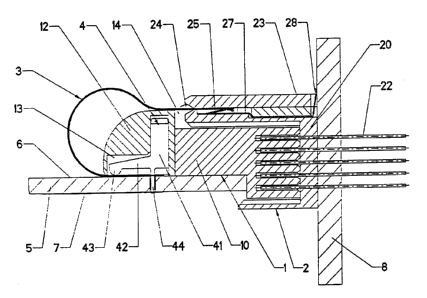
Figure 1 shows a printed circuit board connection in a sectional view with the
plug connectors inserted into each other, the printed circuit board connection
CA 02350289 2001-06-13
- 5 -
being formed from a first, angled plug connector 1 mounted on a printed
circuit
board 5 by means of a mounting surface, and a second, straight plug connector
2
mounted on a printed circuit board 8.
Plug connector 2 is formed with a U-shaped isolating housing 20 having
asymmetrical side legs, the isolating housing having a plug-in portion 21 in
which
pin contacts 22 are arranged in columns and rows. The pin contacts are
inserted at
their opposite ends into bores in a printed circuit board 8.
On the longer one of the side legs of the isolating housing 20 of the plug
connector 2, an isolating holder 23 is provided which can be formed integrally
with the isolating housing 20 or can be formed as separate part and connected
to
the isolating housing.
The plug connector 1 is provided with spring contacts which are not shown in
the drawings. The spring contacts co-operate with the pin contacts 22 of the
plug
connector 2 and form the electrical contacts of the printed circuit board
connection.
The printed circuit board connector 1 is provided with a projection 12 at its
rearward end towards the printed circuit board 5, the projection being
provided
with contact elements 4 which allow an electrical connection between conductor
tracks 6 on the printed circuit board 5 and contact tracks 33 on a flexible
conductor foil 3. The contact elements 4 are guided in recesses 13 in the
projection 12, and the number of contact elements corresponds to the number of
contact tracks on the flexible conductor foil 3. The projection 12 is formed
as
separate part which is attached to the plug connector and to the printed
circuit
board.
The flexible conductor foil 3 which is shown enlarged in Figure2, consists of
a
flexible support foil 30 which is provided on both of its sides with contact
tracks
33, 35 which are also flexible and serve for transmitting electrical signals.
The
conductor foil which is guided in a loop around projection 12, serves as a
second
CA 02350289 2001-06-13
-6-
signal transmission means towards the upper isolating holder 23 of the second
plug connector 2.
Figure 1 shows that the contact elements 4 are provided with a vertically
extending leg 41 arranged within projection 12, and a horizontally extending
spring leg 42. Further, a pin-shaped end 44 is provided which projects over
the
horizontally extending spring leg 42 and protrudes into a bore on the printed
circuit board 5 in order to be electrically connected to a conductor track 7.
The
horizontally extending spring leg 42 is provided with a rounded end 43 at its
side
facing the printed circuit board. Vertically extending leg 41 which is held in
recess 13, in co-operation with pin-shaped end 44 which protrudes into the
bore in
the printed circuit board, elastically biases the rounded end 43 of the
horizontally
extending spring leg 42 towards the surface of the printed circuit board 5.
The flexible conductor foil 3 is arranged between the contact elements 4 and
the printed circuit board 5. The conductor foil has a connection end 32
provided
with round openings 34 into which the pin-shaped ends 44 of the contact
elements
4 engage, whereby the connection end 32 of the conductor foil is held at the
plug
connector 1 when the ends 44 engage into the respective bores in the printed
circuit board 5. Contact elements 4 serve for pressing the conductor foil 3
with its
contact tracks 33, 35 arranged on both sides onto the printed circuit board 5.
The
outer contact tracks 33 of the conductor foil are contacted by conductor
tracks 6
arranged on the upper side of the printed circuit board 5 since they are
pressed
against the conductor tracks by the rounded ends 43 of the contact elements 4.
The inner contact tracks 35 are directly contacted by the rounded ends 43 of
the
horizontally extending legs of the contact elements, the pin-shaped ends 44 of
the
contact elements 4 electrically connecting the contact tracks 35 with
conductor
tracks 7 on the lower side of the printed circuit board 5.
Figure 3 shows the plug connector 1 in an isometrical view in a condition in
which it is not inserted into the complementary plug connector. In this view,
a
second plug-in portion is clearly visible in addition to the conventional plug-
in
portion 11 of the plug connector, the second plug-in portion being formed by
CA 02350289 2001-06-13
-"
means of the conductor foil 3. On a side opposite the printed circuit board,
three
block-shaped holder elements 14 are provided to which the flexible conductor
foil
3 is attached by means of a rivet-like attachment 15. The contact tracks 33,
35 on
the conductor foil 3 are arranged in the free spaces between the holder
elements,
the connection end 33 of the conductor foil being inserted into slot 24 of the
complementary plug connector 2 when the plug connectors are inserted into each
other.
Figure 4 shows the plug connector 2 in an isometrical view, the isolating
housing 20 being formed with asymmetrical, U-shaped legs between which the
plug-in portion 21 with contact pins 22 is provided. Adjacent the longer one
of the
legs of the isolating housing 20, the isolating holder 23 is arranged. The
isolating
holder 23 is provided with a slot 24 having recesses 26. Recesses 26 also
extend
into the corresponding leg of the isolating housing and are adapted to
accommodate the holder elements 14 on the isolating housing 10 of plug
connector 1. Recesses 26 allow to insert the connection end 31 of the
conductor
foil 3 into slot 24 of plug connector 2.
Upon insertion of the plug connectors into each other, connection end 31 of
the conductor foil 3 is inserted into slot 24, whereby the resilient contacts
25
arranged below the conductor foil contact the contact tracks 35 and
simultaneously press the upper contact tracks 33 against the electrical
contacts 29.
Slot 24 is provided with chamfered edges in order to allow insertion of the
conductor foil.
The contact achieved with the contact tracks of the conductor foil is
comparable to that described with respect to the printed circuit board 5. The
contact elements 25 arranged below the flexible conductor foil 3 serve for
transmitting the signals of the lower contact tracks 35, whereas the
electrical
contacts 29 arranged above the conductor foil ser<~e for transmitting the
signals of
the upper contact tracks 33.
CA 02350289 2001-06-13
g
It is here provided to use the lower contact tracks 35 of conductor foil 3 as
shield. To this end, the signals transmitted by means of the contact elements
25
are transmitted to a shielding element 27 made from sheet metal and arranged
in
the interior of the isolating holder 23, these signals being transmitted by
means of
spring contacts 28 formed integrally with the shielding element, to suitable
conductor tracks on the printed circuit board 8.
Figure S shows the isolating holder 3 of the plug connector 2 in an
isometrical
view after being detached from the isolating housing 20, the electrical
contacts 29
being now visible. In the interior of the isolating holder 23, an electro-
optical
converter is arranged which is not visible in this Figure. The electrical
contacts of
the electro-optical converters are connected to the electrical contacts 29,
and the
optical connection of the electro-optical converter is connected to light
guide
fibres 9 protruding from the isolating holder. The isolating holder 23 can
also be
formed integrally with the isolating housing 20 rather than being formed as
separate part which can be attached to the isolating housing.