Note: Descriptions are shown in the official language in which they were submitted.
CA 02350435 2001-06-13
EFFICIENT BATTERY TRANSFER CIRCUIT
Field of the Invention
The present invention relates in general to power transfer and more
specifically to a battery transfer circuit for powering an electronic device
during operating
and power failure conditions.
Background of the Invention
There are many prior art circuits that provide power to an electronic device
to when a connected power supply experiences a power failure or disturbance.
When the power
failure occurs, a battery, located within the electronic device, provides
backup power to the
electronic device. Although the battery is used to provide backup power, prior
art circuits are
unable to inhibit unwanted battery operation. Unwanted battery operation
occurs when the
battery supplies power to the electronic device during normal operating
conditions due to
15 load and line regulation characteristics of the wall-adapter or transformer-
type power supply.
Summary of the Invention
The present invention is directed at a battery transfer circuit for powering
an
electronic device and charging an internal battery from a power supply during
normal
2o operating conditions and for providing back-up power from the internal
battery to the
electronic device when a power failure or disturbance condition is sensed. The
present
invention is also easily adaptable to different power levels and provides a
configurable output
voltage threshold for battery operation as a result of the power failure to
prevent unwanted
battery operation due to line and load regulation characteristics of the power
supply.
25 Another advantage of the circuit of the present invention is that it
provides an
instant transition from power supply, or normal, operation to battery, or
power failure,
operation without transfer circuit delays to overcome an electronic device
reset due to the
voltage drop-out experienced during a power failure. Also, the present
invention provides a
means for increasing battery run time during power failure operation by
switching out series
3o elements between the battery and the electronic device during a prolonged
power failure.
The present invention also includes circuitry to sense the output voltage of
the
power supply to determine when a power failure or disturbance occurs.
According to an aspect of the present invention there is provided:
A battery transfer circuit connected to a load, a power supply for powering
CA 02350435 2001-06-13
2
said load with at least a minimum supply voltage during normal operating
conditions, and a
source of battery voltage for powering said load during a power fail condition
when said
power supply is unable to power said load at said minimum supply voltage, said
battery
transfer circuit comprising:
a first circuit for applying at least said minimum supply voltage to said load
during said normal operating conditions;
a second circuit for charging said battery to an optimal voltage greater than
said minimum supply voltage and for down-regulating said optimal charge
voltage to a
predetermined voltage and for applying said predetermined voltage to said load
during said
1o power fail condition, wherein said predetermined voltage is less than said
minimum supply
voltage.
Brief Description of the Detailed Drawings
Embodiments of the present invention will now be described with reference to
the accompanying drawings in which:
Figures 1 to 3 are schematic diagrams of prior art battery transfer circuits;
Figure 4 is a schematic diagram of a preferred embodiment of a battery
transfer circuit in accordance with the present invention;
Figure 5 is a second embodiment of the battery transfer circuit of Figure 4;
2o Figure 6 is a third embodiment of the battery transfer circuit of Figure 4;
and
Figure 7 is a fourth embodiment of the battery transfer circuit of Figure 4.
Detailed Description of the Preferred Embodiments
Turning to Figures 1 to 3, prior art battery transfer circuits are shown. In a
first
prior art example, as shown in Figure 1, the circuit 10 rectifies and filters
an output from a
power supply 12 via a diode 14 and a capacitor 16. This rectified and filtered
output is then
used to power a regulator circuit 18 which, in turn, provides an optimal
charge voltage to
charge a battery 20 and to power an electronic device 22. In the case of a
power failure or
disturbance, the battery 20 automatically provides a battery charging current
to the electronic
3o device 22. However, when the output from the power supply 12 is converted
to the optimal
charge voltage, a loss in efficiency is experienced due to voltage drops in
the regulator circuit
18. Also, since the battery 20 is directly connected to the regulator circuit
18, control of the
battery charging current is not possible.
CA 02350435 2001-06-13
Limiting the battery charging current as a function of battery size and type
is a
requirement to provide maximum battery service life. In order to satisfy this
requirement, a
typical solution is to add a series impedance between the battery 20 and the
regulator circuit
18 to limit the battery charging current. However, this results in the circuit
10 experiencing a
decreased efficiency and reduced run time, increased battery charging time and
decreased
battery output voltage and current during power failure operation.
The size of the battery 20 may also be pre-selected to set a maximum battery
charging current in relation to the load requirement of the electronic device
22. However, if
the load requirement of the electronic device 22 increases, the size of the
power supply 12
to must also be increased requiring a larger battery to meet the increased
battery charging
current available from the regulator circuit 18.
A second prior art circuit 24 is shown in Figure 2. As before, the output from
the power supply 12 is rectified and filtered by the diode 14 and the
capacitor 16. In this
circuit 24, the rectified and filtered output is directly provided to the
electronic device 22 as
15 well as to the regulator circuit 18 for supplying the optimal charge
voltage to charge the
battery 20. The battery 20 is connected to the electronic device 22 via a
second diode 26
which isolates the battery from unregulated rectified and filtered output and
prevents
overcharging of the battery when the unregulated rectified and filtered output
is at a higher
voltage than the optimal charge voltage of the battery 20. During a power
failure or
2o disturbance, the rectified and filtered output drops below a battery float
voltage (battery
output voltage + (voltage drop across the second diode 26)) and the battery 20
automatically
provides the battery charging current. By directly supplying the rectified and
filtered output
to the electronic device 22, the efficiency loss of a voltage regulating stage
is avoided. As a
result, a smaller power supply 12 may be used. The optimal charge voltage may
also be
25 limited to charge the battery 20 to avoid exceeding its maximum charge
rate. By isolating the
battery 20 from the electronic device 22, this circuit 24 can be adapted to
various power
levels without necessarily having to provide a smaller or larger battery due
to charging rate
requirements. However, in order to avoid unwanted battery operation, the
rectified and
filtered output voltage is required to be higher than the battery float
voltage minus one diode
3o drop under all line and load conditions. The result is that most designs of
this type tend to
operate efficiently at nominal line and load conditions but operates on
battery under low AC
line high load conditions. This results in drastically reduced holdover time
and shortened
battery life. Holdover time is the length of time that the electronic device
is capable of
battery operation before the battery is drained.
CA 02350435 2001-06-13
Yet another prior art circuit 28 is shown in Figure 3. As before, the output
from the power supply 12 is rectified and filtered by the diode 14 and the
capacitor 16. In
this circuit, the rectified and filtered output is supplied to a switch or
relay 30 and a sense
circuit 32 as well as to the regulator circuit 18. The switch or relay 30 is
controlled by the
sense circuit 32. The output from the regulator circuit 18 pravides a optimal
charge voltage
suitable for charging the battery 20. When a power failure or disturbance
occurs, the sense
circuit 32 causes the switch 30 to switch from the rectified and filtered
output voltage to the
battery charging current. This allows operation of the battery 20 to be
controlled by the sense
circuit 32 and to not be subject to voltage regulation characteristics of the
power supply 12.
to Also, the optimal charge voltage can be current limited to charge the
battery 20 without
exceeding its maximum charge rate. By isolating the battery 20 from the
electronic device
22, this design approach can also be adapted to various power levels without
having to
provide a smaller or larger battery due to charging rate requirements.
However, the sense
circuit 32 and the switch 30 cannot instantaneously switch from power supply
operation to
battery operation after the power failure or disturbance is sensed, due to
circuit time delays.
The result is that no power is supplied to the electronic device 22 for a
brief period of time
until the sense circuit 32 and the switch 30 have time to operate and switch
over. Most
electronic devices 22 powered by the power supply 12 do not have sufficient
energy storage
to prevent a reset or loss of data under these conditions. Some designs of
this type attempt to
2o compensate for the time delay in switching from the rectified and filtered
output to the
battery charging current by configuring the sense circuit 32 to switch at a
higher rectified and
filtered output value. This is beneficial during a power failure but has no
effect on transients
and results in unwanted battery operation at low AC line and high load
conditions.
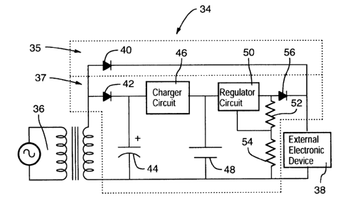
A preferred embodiment of a battery transfer circuit in accordance with the
present invention is shown in Figure 4.
The battery transfer circuit 34 is connected to a power supply 36 and to an
electronic device 38, or load. The battery transfer circuit 34 comprises a
first circuit 35, in
the form of a directly connected diode 40, and a second circuit 37, comprising
a charger
circuit 46 and regulating means in the form of a regulator circuit 50, a first
resistor 52, a
second resistor 54 and a regulator diode 56. The second circuit 37 may also
include a battery
48, an indirectly connected diode 42 and a capacitor 44.
It will be understood that under normal operating conditions, output from the
CA 02350435 2001-06-13
power supply 36 is directly supplied to the electronic device 38 via the first
circuit 35 for
powering the electronic device 38 and when a power failure occurs, the
electronic device 38
is automatically powered by the second circuit 37.
During normal operation, the power supply output is at least a minimum
supply voltage and is rectified by the directly connected diode 40. The power
supply output
varies depending on the AC line and load regulation characteristics of the
power supply 36.
For example, the power supply output could vary from 8 to 20 VDC. Apart from
the voltage
drop across the directly connected diode 40, powering of the electronic device
38 directly
results in efficient operation during the presence of AC input power due to
the lack of any
to intervening power conversion stages.
While the power supply output is powering the external electronic device 38,
the power supply output is also rectified by the indirectly connected diode 42
and filtered by
the capacitor 44 to produce a rectified and filtered output. The rectified and
filtered output is
supplied to the charger circuit 46 which then uses any one of a number of
efficient industry
standard power conversion techniques to provide a charge voltage to charge the
battery 48 to
an optimal charge voltage and an input to the regulator circuit 50. In the
present example,
with a power supply output of 8 to 20 VDC, the optimal charge voltage is 13.6
VDC but may
be adjusted to the requirements of any battery voltage. As mentioned above, by
isolating the
battery 48 from the electronic device 38, the preferred embodiment is
adaptable to various
2o power levels without having to provide a smaller or larger battery due to
charging rate
requirements.
The regulator circuit SO uses an electronically controlled series element,
such
as an industry standard three terminal regulator or equivalent circuit, along
with the resistors
52 and 54 to down-regulate the optimal charge voltage to pravide and set a
predetermined
voltage. The regulator diode 56 isolates the regulator circuit 50 and the
battery 48 to prevent
charging/discharging of the battery 48 by the power supply output. The
predetermined
voltage is set to coincide with the lower, or minimum limit of the supply
voltage, which in
the present embodiment is 8.0 V. Therefore, the output voltage threshold for
battery
operation can be precisely set and no battery charging current flows to the
electronic device
3o 38 until the power supply output drops to less than 8.0 VDC. When the power
supply output
drops below this minimum value, the predetermined voltage is immediately
applied to the to
the electronic device 38. The predetermined voltage is set such that it is
less than the
minimum supply voltage during the normal operating condition.
CA 02350435 2001-06-13
Turning to Figure 5, a second embodiment of the present invention is shown.
Along with the components of the preferred embodiment, the battery transfer
circuit 68
further comprises a sense circuit 70. The input of the sense circuit 70 is the
rectified and
filtered output while the output is connected to a base region 72 of a
transistor 74. The
collector region 76 of the transistor 74 is connected to the second resistor
54 and a capacitor
78.
In order to improve efficiency, the sense circuit 70 is used to turn off the
transistor 74 when a power failure, or disturbance, is sensed which, in turn,
has the effect of
turning the regulator circuit 50 fully ON. The power failure occurs when the
power supply
output drops below the minimum supply voltage value. This reduces the voltage
drop
experienced across the regulator circuit 50 thus increasing the voltage
supplied to the
electronic device 38 and consequently, battery run time. The capacitor 78 is
used to limit the
rate of rise of the predetermined voltage and to reduce transients to control
the load supplied
to the electronic device 38. Unlike prior art control circuits which govern
when the output is
switched from the power supply 36 to battery power, the timing of the sense
circuit 70 is not
critical since its function is to increase the efficiency of the battery
transfer circuit 68 during
prolonged power outages rather than supply instant battery operation in the
event of a power
failure or disturbance.
Yet another embodiment of the present invention is shown in Figure 6.
2o Along with the components of the second embodiment, the battery transfer
circuit 80 further
comprises a bypass sense circuit 82. Input of the bypass sense circuit 82 is
the rectified and
filtered output while the bypass circuit output 84 is connected to a relay or
electronic switch
86.
The bypass sense circuit 82 and the switch 86 operate to short out the
regulator circuit 50 and the regulator diode 56 when a power failure or
disturbance is sensed.
Although the addition of the bypass sense circuit 82 and the switch 86
produces an abrupt
change in the voltage and current supplied to the electronic device 38, the
efficiency of the
battery transfer circuit 80 is further increased by directly connecting the
battery 48 with the
electronic device 38. As with the second embodiment, the timing of the bypass
sense circuit
82 is not critical.
The bypass sense circuit 82 is configurable to provide a two step mode of
operation where the regulator circuit 50 is allowed to turn ON by switching
OFF the
transistor 74 and then turned OFF by turning the switch 86 ON to directly
connect the battery
48 to the electronic device 38. In this embodiment, the increase in the
voltage applied to the
CA 02350435 2001-06-13
7
electronic device during power failure conditions minimizes voltage and
current transients
which may disturb operation of the electronic device 38.
A fourth embodiment of the present invention is shown in Figure 7. Along
with the components of the first embodiment, the battery transfer circuit 88
further comprises
the bypass sense circuit 82 of Figure 6. Input of the bypass sense circuit 82
is the rectified
and filtered output while the output is connected to a base 90 of a transistor
92.
In this embodiment, the transistor 92 is configured to turn ON slowly when a
power failure or disturbance is sensed, such that the voltage drop across the
transistor 92
slowly decreases to a minimum value. Although the voltage drop across the
transistor 92 in
1o the fully ON state is typically higher than across an equivalent relay
circuit, the reduction in
efficiency and battery run time is offset by the elimination of voltage and
current transients
on the output which could disturb the normal operation of the electronic
device 38. This
embodiment is particularly useful in any application where transfer from one
DC power
source to another DC power source is required without switching delays.
It will be appreciated that, although various embodiments of the invention
have been described and illustrated in detail, various changes and
modification may be made.
One such modification is that although only a single diode is shown in each of
the
embodiments, any standard diode configuration could be used to provide a DC
output from
the AC output of the power supply 36. Similarly, the output of the power
supply 36 may be a
2o DC voltage, as in various wall adapter power supplies and therefore, a
standard diode bridge
circuit may be used to provide automatic polarity correction for the
electronic device 38 and
the regulator circuit 50. It will also be understood that the charger circuit
46 may be current
limited so that a maximum amount of power required to charge the battery does
not overload
the power supply 36. All such changes and modifications may be made without
departing
from the sphere and scope of the invention as defined by the claims appended
herein.