Note: Descriptions are shown in the official language in which they were submitted.
CA 02350486 2001-05-10
WO 99/59238 PCT/US99/09260
UNINTERRUPTIBLE POWER SUPPLY WITH PLURALITY OF INVERTERS
The present invention relates to an uninterruptible power supply and
especially to an
uninterruptible power supply (UPS) for use in communication systems or
networks,
particularly wide bandwidth systems and networks, such as cable TV and
telecommunications distribution systems, and to other applications in which
the power
sources of the UPS utilize an inverter for providing power to moderate and low
power loads,
i.e. under about 5 kva, although being applicable to uninterruptible power
supplies
generally.
BACKGROUND OF THE INVENTION
Back up power systems are available which are based on several different
topologies. While many of these are sometimes referred to as uninterruptible
power systems,
strictly speaking they are not. In these so called UPS systems, power from a
first source,
most typically an a.c. power line, powers the load either directly or through
a conditioning
or regulating device such as a ferroresonant transformer. Upon failure of the
first source, a
second source, typically an inverter powered by batteries, is actively
switched into the
circuit to supply the load. Sometimes the first and second sources share a
single
ferroresonant transformer so that the load is always powered by the
ferroresonant
transformer, which in turn is powered by either the first source or, upon
failure of the first
source, the second power source which is switched in to power the transformer.
Two factors
conspire to prevent such designs from providing truly uninterruptible power.
First, it is
necessary to monitor the first power source continuously, and quickly
determine that it has
failed. Given the inherent time variant nature of the sinusoidal wave form
typical of a.c.
power sources, this is very difficult to achieve. Further, once it has been
determined that the
first power source has failed, it is necessary to switch over to the second
power source and
to positively disconnect the first source to assure that power is not fed back
to the first
source from the second. Typically, this switch over and disconnect process is
accomplished
using an electromechanical relay or contactor, which is inherently a slow
device. Allowing
for the time required to first detect failure of the first power source and
then accomplish the
change over to the second source, the output power may be intemtpted for
several tens of
milliseconds. This is acceptable for some loads, but not others.
For sensitive loads, a full time inverter, i.e., a true UPS, is best. In this
known
topology, a single inverter converts d.c. power to a.c. power and supplies it
to the load on a
continuous basis. Generally, power is normally supplied from a first a.c.
power supply,
normally a power line, through a rectifier to provide a first d.c. source
which normally
supplies the d.c. power required by the inverter. This same rectifier keeps
charged batteries
which provide a second d.c. source of power. The second d.c. source is
connected to the
inverter in parallel with the first d.c. source. Upon failure of the first
d.c. source, the inverter
CA 02350486 2001-05-10
WO 99/59238 PCT/US99/09260
continues to be supplied with d.c. power from the batteries. Upon restoration
of the first d.c.
source, the rectifier once again powers the inverter and, at the same time,
recharges the
batteries. Because of the parallel connection of the first source and the
battery across the
input to the inverter, the inverter always supplies a.c. power to the load
with no disturbance
S or interruption of the a.c. output when the first source fails or is
restored.
The advantages of a true UPS include a continuously uninterrupted power output
to
the load, as well as an output whose frequency and wave form are independent
of the input.
This allows the UPS to serve as a frequency converter, for example, providing
stable and
accurate 60 Hz power from a 50 Hz power source, or from a power source having
an
unstable frequency such as an emergency generator. An additional advantage is
that no
switch is required to disconnect the input of the UPS from an a.c. source,
since the inverter
for inverting rectified power from the a.c. source will not feed power from
other power
supplies back through the rectifier.
This true UPS topology, using a dual conversion approach with the a.c. power
being
converted to d.c. power, and then back to a.c. power, is widely used in medium
and large
UPS systems, or those with output ratings above 20 kva or so, as well as small
systems used
in critical applications such as telecommunications.
The main disadvantage of this true UPS approach at lower power ratings has
been
poor e~ciency. The reason for the poor efficiency of the true UPS in smaller
sizes is the use
of batteries, or other power sources, with relatively low d.c. voltages.
Efficiency at low d.c.
voltage is poor, not only because of ohmic conduction losses, but also because
of losses in
the semiconductor switching devices of the rectifier and inverter which have a
relatively
constant on-state voltage drop. A typical 1.0 volt drop across a conducting
transistor, for
example, is an insignificant 0.25% loss in a 400 volt apparatus, but
represents a loss of
nearly 4.2% in a 24 volt system.
The d.c. voltage utilized in a UPS is typically dictated by the cost of the
batteries.
For a given level of stored energy, a string of relatively few large cells is
of significantly
lower cost than a string of relatively many small cells. At the power levels
typical of a
small, single phase UPS in the 1 kva range, for example, batteries are most
economical in
the 24 to 36 volt range, but significantly higher efficiency would be achieved
at a d.c.
voltage in the 400 volt range.
U.S. patent No. 5.010,469 issued on April 23, 1991 to Howard H. Bobry (the
inventor herein) discusses the advantages and the disadvantages of a "true
UPS". The patent
discloses a UPS in which the load is normally supplied with power from an a.c.
power line,
3$ with a battery supplying power upon failure of line power. The power line
is connected
2
CA 02350486 2001-05-10
WO 99/59238 PCTNS99/09Z60
through an isolation transformer to a rectifier which provides a relatively
high voltage d.c.
power source. This d.c. power source is connected to a single primary winding
of a
transformer through inverter circuitry having one input connected to the
relatively high
voltage d.c. power source and another input of the inverter circuitry
connected to a low
voltage d.c. power source, such as a battery, to effect a connection of the
low voltage source
through the inverter circuitry to a common portion of the transformer winding
which is
common to both d.c. sources. Operation of the inverter circuitry at the higher
one of the two
diverse input voltages is achieved through the use of taps on the single
primary winding of
the transformer and is such that the inverter circuitry operates to energize
the primary
winding from the relatively high voltage d.c. source as long as it maintains a
higher voltage
than that of the low voltage power source across the common part of the
primary winding.
Upon a failure of the high voltage source to maintain this higher voltage
across the common
portion of the primary winding, the low power source will supply the power to
the primary
winding until the high voltage power source again establishes a higher voltage
across the
common part of the primary winding .
While the UPS of this prior patent achieves operation at two different
voltages to
provide an increase in e~ciency, the isolation transformer, for the power
supply input to the
high voltage rectifier, adds to the size, weight, and cost of the system and
reduces overall
efficiency of the system. This isolation is needed because of the shared
inverter circuitry and
a common transformer primary winding. Thus an isolation transformer for the
high voltage
power source is required.
In addition, the change over voltage at which the UPS supplies power from a
lower
order voltage source is dictated by the voltage of the lower voltage power
source so that a
lower voltage source cannot be given preference over a higher voltage source
for supplying
power to the load. Moreover the UPS of the patent is not amenable to having
any additional
d.c. power source connected to the common inverter and common transformer
winding.
Among the various objects of the present invention, which will be apparent
from
the description of preferred embodiments, is the provision of a true UPS
topology which: ( 1 )
enables the use of one or more a.c. power supplies, including one or more high
voltage a.c.
power supplies, for establishing one or more high voltage d.c, power sources
for the UPS;
(2) enables the order of preference (priority) for d.c. power sources of the
UPS to be in
accordance with or different from the order of the voltage levels of the d.c.
sources and in
accordance with the magnitude of an effective voltage established for each
d.c. power
source; (3) enables the establishment of an order of preference for the
d.c.power sources
which have substantially the same voltage level; (4) enables an order of
preference for the
3
CA 02350486 2001-05-10
WO 99/59238 PCT/US99/09260
d.c. power sources to be established by effective voltages for the d.c. power
sources which
approximate a desired output voltage from the UPS; (5) enables the setting of
the effective
voltages to a voltage higher than a desired output voltage with the output
voltages being
regulated to the desired output voltage; (6) enables the easy addition of one
or more power
supplies to a UPS; (7) enables the maximizing of efficiency of the transistors
and the
inverters of the UPS as well as cost reduction in providing isolation for the
power supplies
from each other and the output of the UPS to thus maximize overall system
efficiency while
reducing costs.
SUMMARY OF THE INVENTION
The present invention provides a true uninterruptible power supply for
supplying
power to a toad from any one of a plurality of independent d.c. power sources
in a
predetermined sequence. The independent power supplies may comprise one or
more d.c.
sources which are established by a battery or a battery bank, and one or more
d.c. sources
which are established by rectifying a.c. power from a.c. power lines or from
other a.c. power
supplies.
The power sources are separately connected to the inputs of separate
inverters, one
for each power source. The outputs of the inverters are separately connected
to a voltage
converting means for converting the voltages of the inverter outputs to
selected different
predetermined effective a.c. voltages which determine the sequence in which
the power
sources are to supply power to the load, with the operating effective voltage
which is higher
than any other establishing a back biasing voltage for each power source which
produces a
lesser converted effective voltage whereby the power source and its inverter
providing the
higher than any other effective voltage supplies power for the load.
In the preferred embodiments of the invention, the output of each d.c. power
source
of the UPS is directly connected to a corresponding inverter, which is
separate from any
other inverter, and the outputs of the inverters are each connected to
energize a voltage
converter having separate transformer primary windings, one for each inverter,
to provide a
separate transformed secondary effective voltage for each inverter and its
corresponding
power source. The effective voltages have different predetermined magnitudes
which may
approximate the desired voltage for the load with the magnitudes of the
effective voltages
determining the order in which the d.c. power supplies are used to supply
power to the load,
the preferred source for normally supplying the power having an effective
voltage which is
higher than any other effective voltage.
In the preferred embodiments, the transformer primary windings for the
inverter
outputs have a common secondary configuration. The common secondary
configuration
4
CA 02350486 2001-05-10
WO 99/59238 PCT/US99/09260
may comprise, for example, a separate secondary winding for each of the
primary windings
with the secondary windings being connected in parallel with each other so
that the
secondary effective voltage higher than any other is established as the
secondary voltage for
al) secondary windings.
Instead of separate secondary windings for each primary winding which are
connected to provide a common secondary, the primary windings for the outputs
of the
inverters may have a common core with a single secondary for all primaries.
Any other
equivalent secondary or transformer structure to that described may be
utilized.
In accordance with the preferred embodiments, the desired magnitudes for
effective
voltages for the respective power sources are obtained by setting the primary
to secondary
turn ratios to provide effective voltages having relative magnitudes which
establish the
desired order in which the power sources are to be used to supply power to the
load. The
magnitude of the effective secondary voltage of each power source being such
that, when a
power source is supplying the load power, its secondary effective voltage
establishes a
primary voltage on the primary windings of the other power sources which is
sufficient to
back bias any power source with a lesser effective voltage against supplying
load power to
its corresponding inverter. When the back-biasing voltage on the primary
winding for any
power source drops to or slightly below the voltage output of the power source
to the
inverter for the winding, that power source will supply power to the load
until it is again
back biased by the operation of a higher order power source.
To provide the desired secondary effective voltages, the primary to secondary
turns
ratios for the transforming of the outputs of the inverters are set to
establish secondary
effective voltages with relative magnitudes corresponding to the desired order
in which the
d.c. sources are to be used to supply power to the load. The predetermined
magnitudes for
the effective voltages are also such that each is sufficient to establish the
back biasing of any
power source having a lesser effective voltage. When the secondary voltage of
the preferred
source drops to or slightly below the effective voltage of the next preferred
d.c. power
source, the next preferred power source will no longer be back biased and will
start
supplying the UPS power for the load.
In operation, all inverters of the UPS operate simultaneously. The effective
voltages
of the power sources preferably approximate each other to enable a following
source to
quickly assume the function of supplying the load when the preceding power
source is
failing.
The independent inverters, one for each power source, are synchronized and
operate
continuously and in parallel with each other.
5
CA 02350486 2001-05-10
WO 99/59238 PCT/US99/09260
In the illustrated embodiments of the invention, one uses two or more
transformers,
one for each of the inverters. Another embodiment has a single transformer
incorporating
two or more primary windings, one for each of the inverters.
These and other aspects and advantages of the present invention will be
readily
understood and appreciated by those skilled in the art from the following
description of the
preferred embodiments for practicing the invention in view of the accompanying
drawings.
BRIEF DESCRIPTION OF THE DRAWINGS
FIG. 1 is a schematic diagram on an uninterruptible power supply according to
one
embodiment of the invention.
FIG. 2 illustrates a pulse width modulated inverter wave form.
FIG. 3 is a schematic diagram of an uninterruptible power supply according to
another embodiment of the invention.
DESCRIPTION OF PREFERRED EMBODIMENTS
The preferred embodiments of the invention for an uninterrupted power supply,
are
described and illustrated using certain inverter designs for the preferred
modes of operation.
Those skilled in the art will fully understand from the structure and
operation of the
preferred embodiments disclosed and described, and will appreciate, that the
present
invention can be practiced using many different inverter designs which convert
d.c. power
to a.c. power. Such inverter designs include the H-bridge inverter as
illustrated herein, as
well as center tapped, parallel, half bridge, and other inverter designs as
are known in the art
or may be later developed. Similarly, while the use of field effect
transistors (FETs) is
shown, for simplification of the drawings, other switching devices such as
bipolar
transistors, insulated gate bipolar transistors (IGBT s), or any other device
having
appropriate characteristics for the intended application may be used.
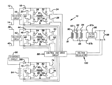
In the embodiment of Fig. l, a UPS apparatus 10 is shown as having two
independent a.c. power supplies. Power lines 12, 14 from a first a.c. power
supply provide
power input to a rectifier circuit 16 to provide a first d.c. power source.
The rectifier 16,
may be a conventional rectifier circuit such as a switchmode power supply, a
phase
controlled rectifier, a controlled ferroresonant rectifier, a power factor
controlled boost
circuit, or any other suitable rectifier known in the art. The rectifier need
not incorporate
isolation means, as isolation of the power supplies from each other and the
output will be
provided by the UPS apparatus of the invention as will be appreciated from the
further
description of the preferred embodiments.
The d.c. output current of rectifier 16 is conducted through diode 18 to the
input of
an inverter A comprised of transistors 20, 22, 24, and 26. Inverter A is of
conventional
6
CA 02350486 2001-05-10
WO 99/59238 PCTNS99/09260
design. In inverter A, transistors 20 and 26 are rendered conductive to
provide one half
cycle of an a.c. output of the inverter and transistors 22, 24 are rendered
conductive to
provide the alternate half cycle. The purpose of diode 18 is to prevent a
backwards, or
reverse, flow of current from the inverter to the rectifier, and may not be
necessary with
some rectifier designs. Where diode 18 is not required, it may simply be
omitted. Diodes 28,
30, 32, and 34 provide paths for reverse current flow through the inverter,
thus allowing
operation in all four quadrants so that the inverter may power reactive loads,
as is well
known and understood. These diodes may be separate and discrete components, or
may be
integrated with transistors 20, 22, 24, and 26.
The inverter A drives a transformer primary 36, which has an associated
transformer secondary 90. The primary 36 and the transformer secondary 90,
while shown
spaced in the schematic, as is conventionally done, have a common transformer
core 91, the
core being schematically shown along both the primary 36 and the secondary 90.
A second a.c. power supply comprises a.c. power lines 38, 40. In a manner
similar
to that described for the first power source, the power lines 38, 40 are
connected to the input
of a rectifier circuit 42 to provide a second d.c. power source. The output of
the rectifier
circuit 42, supplies d.c. current, through (optional) diode 44, to the input
of an inverter B
comprised of transistors 46, 48, 50, and 52, and diodes 54, 56, 58, and 60
which operate as
described for the corresponding transistors 20, 22. 24, and 26, and
corresponding diodes 28,
30, 32, and 34 of inverter A.
The output of the second inverter B drives a separate primary 62 of a second
transformer, the primary 62 having an associated transformer secondary 92. As
before, the
transformer primary winding and the transformer secondary winding have a
common
transformer core 93. This second transformer is separate and distinct from the
previously
described first transformer driven by the first inverter.
A third inverter circuit C follows the structure of the other inverters and is
comprised of transistors 70, 72, 74, and 76, and diodes 78, 80, 82, and 84.
The input to the
third inverter circuit C is connected to the output of a third power supply
comprising a
battery 64. The connection from the battery to the input of the inverter
circuit is shown as
having a diode 68. This inverter drives a third transformer primary ~6 of a
separate
transformer, the primary having a common core 95 with a transformer secondary
winding
94.
A battery charger circuit 66 maybe be connected across the diode 68 to be
powered
by current flowing from the primary winding 86 through the third inverter to
the battery
charger when the UPS is powered by either the first or the second a.c. power
source. As
7
CA 02350486 2001-05-10
WO 99/59238 PCT/US99/09260
explained in more detail hereafter, when the UPS supplies power through either
the first or
second inverter, the primary winding 86 will have a secondary to primary
transformed
voltage thereon which will back bias power flow from the battery. This back
biasing voltage
will also operate through the inverter C to supply power to the battery
charging circuit to
S keep the
battery charged. This powering of the battery charging circuit is such that it
does not
interconnect the inverters or their power supplies, nor does it affect the
isolation of the
inverters and the UPS output since the back biasing voltage is established on
the primary 86
by transforming the output voltage of the secondary as will be well
understood, from the
description herein and the drawings, by those in the art. As an alternate, a
separate battery
charger operating independently of the inverter circuits may be provided (not
shown).
All three inverter circuits are driven in synchronization with each other by a
control
and drive circuit 88 in a manner well known in the art so that each inverter
produces the
identical wave form as the other two inverters, differing only in magnitude.
The inverter
wave forms may be a simple square wave, or may be a pulse width modulated wave
form
which is controlled to provide a regulated output voltage and/or a desired
output wave
shape. A filter circuit 96 may be used to further control the shape of the
output wave form
produced at output terminals 98. The filter circuit may be a simple LC circuit
comprised of a
series inductor and a parallel capacitor, or may be a more complex circuit as
required by the
specific application. For some applications, the filter circuit may be
omitted.
The control and drive circuit 88 may be isolated from the inverters and the
UPS
output via the use of isolation transformers, optical couplers, or other
suitable means well
known in the art. Similarly, isolating means may be used to supply power to
the control and
drive circuit 88 from each of the power supplies for the UPS. As is
conventional practice,
connections (not shown) are made to the power lines 12, 14, and 38, 40 for the
rectifiers 16
and 42 and to the battery 64 to establish individual d.c. sources (not shown)
for powering
the control and drive circuit. The outputs of these d.c. sources are ORed in a
well known
manner to supply to the control and drive circuit whenever one or more of the
power
supplies for the UPS are available, i.e., are functional to supply power.
While inverters A, B, C, have been described as having the same design, and
operating in the same manner, it will be understood that the present invention
allows the
transistors and the inverter designs for the inverters to be different to
maximize the
efficiency of the respective inverters at the applied voltage.
In accordance with the present invention, the secondary transformed voltages
constitute effective voltages for the d.c. power sources and the
transformation ratios for the
8
CA 02350486 2001-05-10
WO 99/59238 PCT/US99/09260
primaries are such as to provide secondary effective voltages of magnitudes
which are different from each other and which approximate the desired output
voltage for
the UPS. The relative magnitudes of the effective voltages will determine the
order of
preference in which the respective d.c. power sources operate to supply load
power from the
UPS. The most preferred d.c. source, i.e. the one chosen for normally
supplying power from
the UPS, has a transformed voltage higher than that of any other and which
operates to reverse bias all other d.c.sources, with each other d.c. power
source assuming the
function of supplying power to the load through the UPS when its effective
voltage becomes
higher than any other and it will continue to supply power for the load until
a d.c. power
source of higher order reestablishes a higher effective voltage.
As noted above, the UPS output will, at any time, normally be powered by the
preferred inverter, when it is available, because it is the one having an
effective voltage
higher that any other d.c.power source. This effective voltage will cause all
other primaries
to reverse bias their power sources, whether rectifiers or batteries, or any
other type of d.c.
source, and prevent the power sources from supplying current to their
respective inverters. If
the preferred power source fails, another inverter and its power source
becomes the most
preferred and automatically and naturally, without any action by a control
circuit, provides
the power for the load. This operation is similar to the use of diodes to "OR"
d.c. power
sources together to supply power to an inverter so that the power source
having the highest
voltage will supply power to the load but upon failure of that voltage source
the voltage
source having the next highest voltage will assume the load. By using an
inverter for each
power supply and effectively OR-ing together the transformer outputs for the
inverters, the
power supplies or sources for the inverters may be isolated from each other as
well as from
the a.c. output of the UPS to allow, for example, the use of low voltage
batteries as one
power source which are safely isolated from a high voltage power line used as
another
voltage supply. As will be understood by those skilled in the art from the
foregoing, this
isolation may be accomplished since each primary winding is dedicated to one
d.c. power
source and the inverter for that power source and there need not be any
connections between
inverters. In addition, the rectifiers will block any feed back from the
primary windings
when a primary is back biasing its corresponding d.c. source.
As noted, adjustment of transforming ratios allows any desired order of
preference
for the power sources to be set by design, even to render as the most
preferred power source,
one which has a lower voltage than a lesser preferred power source. For
example, a most
preferred power source may be from a first a.c. power line which is of lower
voltage than a
second a.c, power line of higher voltage but which is preferred only as an
alternate to the
9
CA 02350486 2001-05-10
WO 99/59238 PCT/US99/09260
first power line.
It will also be understood that the voltage of a d.c. power source may be
changed,
for example, by boosting the voltage when rectifying a.c. power, to change the
secondary
effective voltage for the d.c. power source. This provides flexibility not
only when
designing a UPS in accordance with the present invention, but also facilitates
later
modifying the order of preference in the UPS as well as the addition of power
sources,
particularly when using power supplies of substantially the same voltage. An
example may
provide useful clarification of circuit operation. Assume that the first
rectifier circuit 16
produces a regulated d.c. output of 400 volts, (the rectifier may provide d.c.
power either
lower or higher than the a.c. supply). Further assume that the UPS output is
to be a 60 volt
square wave, typical of that required for powering broad band communications
networks
over coaxial cable. The inverter comprised of transistors 20, 22, 24, and 26
will provide a
400 volt square wave across transformer primary 36, while a 60 volt square
wave is desired
across transformer secondary 90. This is accomplished by setting the primary
to secondary
turns ratio in accordance with the transformer equation:
V~s = ~S~
where V is voltage and subscript P indicates primary, s indicates secondary, R
is turns ratio
and ps indicates primary to secondary turns ratio. Accordingly the Rps for the
first
transformer with 400 volts on the primary, and a secondary voltage of 60
volts, will be
400/60, or 6.66/1.
Assume that the second rectifier circuit 42 produces a regulated d.c. output
of 360
volts. The turns ratio between the second transformer primary 62 and the
second transformer
secondary 92 should be 360/60, or 6.00/1. Similarly, given the nominal voltage
of the
battery 64 as 36 volts, the turns ratio between the third transfonmer primary
86 and the third
transformer secondary 94 should be 36/60, or 0.60/1 so that a 60 volt output
can be supplied
from the 36 volt battery.
It will be recognized that all three transformer secondaries, 90, 92, and 94
are
connected in parallel across the secondary output connections 97a, 97b, and
thus all have the
same voltage, i.e. the secondary effective voltage which is higher than any
other. With the
first a.c. power supply available, the first rectifier circuit 16 provides a
400 volt d.c. source
for the first inverter, which in turn produces a 400 volt a.c. square wave
across transformer
primary 36, resulting in a 60 volt a.c. square wave across all three
transformer secondaries.
With a secondary voltage of 60 volts across the secondary winding of the
second
transformer, the voltage across the primary 36 of the second transformer, as
given by the
above equation, will be 60 x RQS or 360 volts, the assigned primary to
secondary turns ratio
CA 02350486 2001-05-10
wo ms9~g pc~r~s99ro9~o
having been 6.00/1, Thus, with the assigned turns ratio the voltage will be
the same voltage
as its d.c. source, i.e. the rectifier circuit 42. A slight difference in
voltage at either the first
rectifier circuit 16 or the second rectifier circuit 42 would determine which
of the two
sources would supply the load, but it is preferred that the first power source
supply power
for the load when it is available. This can be assured by adjusting the turns
ratio of our
second transformer slightly. By making the turns ratio 6.10/1, rather than
6.00/1, the
secondary voltage for 360 volts on the primary 62 will be 360/ 6.10, or 59
volts. This is
lower than the 60 volts of the first transformer but when the first power
source supplies the
power, the secondary voltage of 60 volts of the first transformer, is now
transformed by the
second transformer with a secondary to primary turns ratio of 1/6.1, and the
above equation
now becomes VP = 60 x 6.1, and a voltage of 366 volts is established across
the primary for
the second power source. This exceeds the 360 volt level of the output of the
second
rectifier circuit 42, so no current will flow from this second rectifier
circuit. All of the power
required will be supplied by the first power source, as desired. If the first
power source fails,
power will then flow from the second power source, via second rectifier
circuit 42. With the
primary/secondary turns ratio of the second transformer now at 6.10/1, the
secondary
effective voltage of the second power source will be 360/6.10, or 59 volts and
the second
power source will operate to supply power for the load when the voltage on its
secondary is
59 volts. This does not provide the 60 volts desired for the load, but we will
discuss this in
more detail later.
Similarly, the 60 volt level from the first transformer, when it is available,
will be
across the third transformer secondary 94. With the assumed battery voltage of
36 volts and
an assigned primary to secondary ratio of .60/1, 60 volts on the secondary of
the third
transformer would transform to 36 volts
across the primary winding for the battery, which is again the same as the
assumed nominal
voltage of the d.c. power source, i.e. the battery . This again needs to be
adjusted slightly to
prevent power flow from the battery at 36 volts as was done for the second
power source.
By making the primary to secondary turns ratio 0.62/1, the secondary voltage
from the
battery will be 58 volts. With this primary/secondary turns ratio, when the
secondary for the
battery transformer has 60 volts across it from the first transformer, the
voltage across the
third transformer primary 86 will be transformed with a transformation factor
of .62 to
provide 37.2 volts across its primary. When the voltage across the secondaries
is from the
second power source, 59 volts, the voltage on the primary for the battery will
be 36.6 volts.
Either voltage would block current flow from the battery to its primary
winding.
11
CA 02350486 2001-05-10
WO 99/59238 PCTNS99/09260
Thus far the circuit of Fig. 1 provides an output voltage which will vary from
58
volts (battery) to 60 volts (first source), depending upon the power source.
This is
satisfactory for many applications. However, some applications need a better
regulated
output voltage including those which require adjustments for the nominal 36
volt battery
which thus far has been assumed to be operating at 36 volts. This battery will
not operate at
a constant 36 volts. Battery voltage will, in fact, typically vary from about
42 volts at full
charge to about 32 volts when fully discharged. A feature of the present
invention, is that the
turns ratios may be further adjusted so that the third transformer will have
no power flow
from the battery when its voltage is as high as 42 volts, and the voltage
across transformer
secondaries 90, 92, and 94 is as low as 59 volts.
This adjustment results in a turns ratio for the third transformer of 0.72/1.
With this
turns ratio, operation from a fully charged battery at 42 volts would result
in a secondary
voltage of 58.3 volts. However, when operating from a discharged battery at 32
volts this
would result in a secondary voltage of 44.4 volts. The output voltage of the
UPS could thus
vary from 60 volts to 44.4, depending on which power source is being used and
the state of
the battery.
A regulated output, constant regardless of the power source or state of charge
of the
battery, may be provided through a voltage regulator. The UPS of Fig. 1
utilizes a voltage
regulator 100 which utilizes pulse width modulation. Using pulse width
modulation in a
well known manner, the voltage regulator circuit 100 monitors the output
voltage of the
UPS and controls the duty cycle of the inverters to maintain a constant and
well regulated
output voltage.
Fig. 2 illustrates the inverter voltage wave forms resulting from the use of
pulse
width modulation. As is conventional, each half cycle of the wave form may be
comprised
of a single pulse, either positive or negative on alternating half cycles with
the instantaneous
voltage of the inverter being controlled by changing the width of the pulse
whereby the
instantaneous voltage during each half cycle of the inverter is either
positive or negative, or
zero as shown in Fig. 2.
With reference to Fig. 2, a voltage wave form 110 as shown would appear across
transformer secondaries 90, 92, and 94 when the UPS is operating from battery
64 at its low
voltage, such as 32 volts in the given example. Wave form 112 of Fig.2 is a
typical voltage
wave form which would appear across the transformer secondaries when the >.JPS
is
operating from the second power source, and wave form 114 is a typical voltage
wave form
which would appear across the transformer secondaries when the UPS is
operating from the
first power source. While the three voltage wave forms shown in Fig. 2 differ
in shape,
12
CA 02350486 2001-05-10
WO 99/59238 PCT/US99/09260
voltage regulator circuit 100 is used to adjust pulse width so as to maintain
a constant
voltage output at terminals 98. Such regulator circuits are well known and no
further
description is necessary to those working in the art. Filter circuit 96 will
function to assure
that the output voltage wave form approximates a square wave, or a sinusoidal
wave form,
or such other wave form as may be desired in a specific application. It will
be understood by
those versed in the art that the desired regulation by pulse width modulation
may also be
achieved by varying the widths of multiple pulses per half cycle, as is well
known.
Returning to our example, the turns ratio for the battery 64 based on a fully
charged battery
was adjusted to 0.72/1 to have no power flow from a fully charged battery
voltage of 42
volts. However, with the ratio of 0.72/1, the battery 64 at its minimum
voltage of 32 volts,
and the wave form 110 of maximum pulse width, as shown in Fig. 2, the UPS
output voltage
will be 44.4 volts. The output voltage when operating from either the first or
second power
source could be regulated down to that same 44.4 volt figure by the use of
pulse width
modulation of Fig. Z. But this would provide a regulated 44.4 volt UPS output
when a 60
volt output is specified. This can be achieved by making a further adjustment
to the
transformer turns ratios to boost the UPS output voltage to 60 volts. To do
this, all of the
turns ratios are adjusted by dividing them by a factor of 60/44.4, i.e. I .35.
This factor is the
desired output voltage for the UPS (60 volts) divided by the effective voltage
of 44.4 for the
battery when operating at a low charge (32 volts) with a transformer
primary/secondary
turns ratio of 0.72/1), which is the turns ratio set for the battery at full
charge (42 volts).
Dividing all the turns ratio by 1.35, the turns ratio of 6.66/1 for the first
transformer is now
4.93/1; the ratio 6.10/1 for the second transformer is now 4.52/1 and the
third transformer
ratio 0.72/1 is now 0.53/1. This sets the primary turns ratios for all power
supplies lower to
provide higher than the 60, 59, and 58 volts for the secondary voltages of the
first and
second sources, and the battery when operating at 42 volts, the effective
voltage for a
battery operating at 32 volts being slightly above the desired 60 volts for
the secondary
voltage.
The secondary voltages for the transformers will now be about 81.1 for the
first
transformer, about 79.7 for the second transformer, and about 79.3 for the
third transformer
with the battery operating at 42 volts and about 60.4 volts when the battery
is operating at
32 volts. It will be noted that the effective secondary voltage for the second
transformer is
more than one volt lower than that of the first transformer and only 0.3 volt
higher than that
of the battery effective voltage when at 42 volts. Depending on the voltage
regulation of the
first and second d.c. power sources it may be advantageous to use a 4.5/1
turns ratio for the
primary of the second transformer for the second power source to provide an
effective
13
CA 02350486 2001-05-10
WO 99/59238 PCTIUS99/09Z60
voltage of 80 volts which is about 1.1 volts below that for the first power
source and about
0.7 volt higher than that for the battery source when operating at 42 volts.
These effective voltages, all of which exceed the desired 60 volts for the
UPS, are,
by using voltage regulation as described, regulated down to the desired 60
volts to maintain
the desired output voltage for the UPS for all power sources. The order of the
magnitudes
for the effective voltages of the power sources are maintained so that the
order of preference
for supplying power from the UPS apparatus is also maintained. It will be
noted that for the
voltage regulation described, the power source which is the less preferred of
all power
sources is assigned an effective voltage which is less than any other
effective voltage and
the primary/secondary turns ratios are set so that the power source which is
preferred less
than any other has an effective secondary voltage which is a little higher
than the desired
load voltage, with all effective voltages higher than the desired load voltage
being regulated
down to the desired voltage.
Figure 3, illustrates a modification of the UPS of Figure 1 and is a preferred
embodiment of the present invention. The embodiment utilizes the same power
supplies,
rectifiers inverters and diodes of the embodiment of Fig. 1. These function as
in
Fig. 1 to energize an individual primary for each inverter. Accordingly, the
circuitry has
been given the same reference as in Fig. 1. However, the three transformer
primaries 36, 62,
and 86 shown in Fig. 1 are replaced with three transformer primaries 102, 104,
and 106.
Whereas the three transformer primaries of Fig. 1 are each closely coupled
magnetically to
an individual one of associated transformer secondaries 90, 92, and 94
respectively using
three separate transformer cores, the three transformer primaries of Fig. 3
are closely
coupled magnetically to each other with a single transformer core 107 having a
single
transformer secondary 108 constituting a common secondary for the primary
windings. The
secondary 108 is connected to the filter circuit 96 and thence to the output
terminals 98. All
components of the embodiment of Fig. 3 operate in the same manner as in Fig.
1, but have a
common core 107 for the primary and secondary windings with a single secondary
108
replacing the three parallel connected secondary windings of the first
embodiment, this
being the full equivalent to the parallel connected secondaries as is well
known by those in
the art. The turns ratios for the primary windings and voltage regulation are
the same in both
embodiments.
The transformer secondary of the embodiment of Fig.3 need not be closely
coupled
magnetically to the transformer primaries. The transformer may in fact
comprise a
fen oresonant transformer, or a controlled ferroresonant transformer, both
well known in the
art, in which case the functions of the filter circuit 96 and the voltage
regulator circuit 100
14
CA 02350486 2001-05-10
WO 99/59238 PCT/US99I09260
are provided by the transformer, so the separate filter circuit and voltage
regulator circuit
may be omitted. As an alternate, the voltage regulation circuit may be
retained for use with a
ferroresonant transformer, thus regulating the primary voltage of the
transformer and
enhancing its efficiency.
Further, it is understood that a UPS according to the present invention may be
operated to provide any output frequency, voltage, or wave form suitable for
the intended
application, and with the addition of a bridge rectifier across the output
terminals 98, as is
well known, a d.c. output may be obtained.
While UPS embodiments comprising three inverters have been described, it is
understood that these are exemplary of the best modes, and that any number of
inverters
greater than one may be used. Most typically, a UPS according to the present
invention
would use two inverters, one operating from a first power source such as the
commercial
power line, and the other operating from a second power source such as a
battery. It is
understood that additional power sources, either a.c. or d.c., may be
incorporated using a
I S separate inverter and transformer primary for each added power source. A
UPS may, for
example, be comprised of a first inverter for operation from a first power
source such as an
a.c. power line, a second inverter for operation from a second power source
such as an a.c.
generator, a third inverter for operation from a third power source such as a
fuel cell, a
fourth inverter for operation from a fourth power source such as an array of
photo voltaic
cells, a fifth inverter for operation from a fifth power source such as a
battery, and so on.
Preferably, for efficiency, the UPS will be set to naturally and automatically
select the
available power source which allows operation via the inverter having the
highest input
voltage available, thus resulting in maximum efficiency at all times
consistent with the
power sources available. The apparatus can be designed such that it is of
modular
construction, allowing additional inverters and primary windings to be added
as additional
power sources are made available, and allowing inverters to be removed for
maintenance or
as power sources become unavailable.
The present invention thus provides a true uninterruptible power supply having
a
plurality of inverters for operation from a plurality of power sources, the
power sources
being selected naturally and automatically to operate the UPS from available
power sources
in a sequential predetermined order of preference which may differ from the
sequential
order of the voltage magnitudes of the power sources, with the order of
preference being
typically determined so as to maximize efficiency. It will be understood from
the foregoing
that the separate outputs of the inverters are connected to a common power
output by
circuitry which establishes an effective voltage for each inverter with the
effective voltages
CA 02350486 2001-05-10
WO 99/59238 PCTNS99/09260
being of different magnitudes and preferably approximating the desired voltage
for the load.
In the described circuitry, the output from the parallel connected secondary
windings of Fig.
1 and the single secondary winding of Fig. 3 each provide a common power
output for the
preferred embodiment.
It is also to be understood that the effective voltages described herein are
those
voltages which would actually exist from an operating power source at the
common output
of the transformer secondary if there is no modification as by voltage
regulation. However,
the effective voltages can differ from the desired load voltage within the
range of voltage
regulation as illustrated in the example in which the turns ratios are
adjusted to provide a
desired effective secondary voltage for a battery at its fully charged voltage
and a different
desired effective voltage at its fully discharged voltage, with all effective
voltages being
regulated down to the desired load voltage. Moreover, the effective voltage,
which is that
determined by the primary to secondary turns ratio for a given voltage of the
d.c. source,
will vary with voltage variations of the d.c. source. Preferably, the primary
to secondary
turns ratios for the effective voltages are set to accommodate the normal
voltage variations
of the d.c sources for supplying power and to provide the described back
biasing voltages
for lower order power sources.
It can also be seen from the foregoing that the present invention ORs the
separate
simultaneously operating inverters for the separate power supplies to
establish one of the
inverters as the inverter for supplying power to a load. This ORing is
accomplished by
providing separate inverters for the power sources and connecting the outputs
of the
inverters to separate transformer primaries to establish different effective
secondary voltages
for the inverters, the secondary voltages having a common secondary for ORing
the
inverters so as to supply load power from one inverter, i.e., the inverter
with an effective
secondary voltage higher than any other inverter with an operative power
supply, the other
operable power supplies of lower order being back biased by the higher
effective secondary
voltage. It may also be seen that by using separate inverters for the power
sources and
separately transforming the outputs of the separate inverters, the UPS of the
present
invention maintains isolation between the power sources and between the power
sources and
the load.
Various aspects of the invention will also be appreciated from the foregoing
description of preferred embodiments. Among others, it will be appreciated
that the present
invention enables the use of one or more a.c. power supplies in a UPS having
an a.c. output,
including one or more high voltage a.c. sources. Further, it enables the order
of preference,
or priority, for the d.c. power sources of the UPS to be different from the
order of the
16
CA 02350486 2001-05-10
WO 99/59238 PCTIUS99/09260
voltage levels of the d.c. sources. It also enables an order of preference for
d.c.power
sources having substantially the same voltage level to be established.
Moreover, it enables
each d.c. power source to establish an effective secondary voltage which
approximates the
desired voltage for the load. And with voltage regulation, the effective
voltages may be set
sufficiently higher than the desired output from the secondary, as described
herein, to effect
voltage regulation to the desired secondary output voltage for all
d.c.sources. It also reduces
the cost of and losses in the UPS system by reducing isolation costs and loses
associated
there as well as enabling the inverters to be designed for the voltages of the
individual
power sources.
Moreover the present invention also provides an improved method of supplying
continuous uninterruptible power to a load. In the method, load power is
supplied from one
of a plurality of independent d.c. sources which have nominal voltages and
which are to be
used in a predetermined order initially and on power failure.. In the method
of the preferred
embodiments, a primary to secondary transforming ratio is established for each
power
source for transforming the inverted voltage from the power source to an
effective
secondary voltage with the primary to secondary transfon~nation ratios for the
power sources
being such that the effective voltages of the power sources have different
magnitudes with
the magnitudes defining a sequential order corresponding to the sequential
order in which
the d.c. power sources are to be used to supply power to the load, and the
magnitudes of the
effective voltages for the power sources are such that each power source
higher in the order
of preference than another has an effective secondary voltage of a magnitude
which will
back bias the next lower order power source against supplying power, thereby
establishing
the operative d.c. power source having a secondary effective voltage higher
than any other
as the power source which supplies load power.
It will be understood that the effective secondary voltage for a power source
and its
inverter and primary is the secondary voltage which would be produced using
primary to
secondary turns ratios as described. If there is no voltage regulation, the
secondary output
voltage is the effective secondary voltage for each power source when it is
supplying the
power.
As will be understood by those in the art, when pulse width modulated voltage
regulation as described is used to regulate the secondary output of the
transformers to a
desired load voltage, the regulated secondary voltages contain instantaneous
voltages of the
magnitude of the effective voltages so that the instantaneous voltages of the
effective
voltage higher than any other will establish the back biasing of the lower
order power
sources. Other known voltage regulators equivalent to that described may also
be used.
17
CA 02350486 2001-05-10
WO 99/59238 PCT/US99/09260
As generally used, high voltage power sources are generally power sources
having a
voltage of at least about 170 volts, but normally 200 volts or over, with a
low voltage source
having a voltage of up to about 70 volts and a moderate voltage source being
between the
high and low voltage sources.
While the invention has been shown and described with respect to specific
embodiments thereof, it has been for the purpose of illustration rather than
limitation, and
other variations and modifications of the specific embodiments herein shown
and described
will be apparent to those skilled in the art and within the scope of the
invention claimed.
18