Note: Descriptions are shown in the official language in which they were submitted.
CA 02350705 2001-05-11
1
Specif ication
NON-CONTACT DATA CARRIER AND IC CHIP
BACKGROUND OF THE INVENTION
Field of the Invention
The present invention relates to a non-contact data carrier
having an antenna coil and an IC chip and an IC chip used for
the same and more particularly to a non-contact data carrier and
an IC chip for surely realizing continuity between the antenna
coil and the IC chip.
Description of the Related Art
A non-contact data carrier having an antenna coil and an IC
chip is conventionally used in the distribution system. Such a
non-contact data carrier is used, for example, by attaching to
a shipping box of a product or a product itself.
The non-contact data carrier generally has a resin substrate,
a metallic antenna coil installed on the resin substrate, and
an IC chip connected to the antenna coil.
When electromagnetic waves are sent to the non-contact data
carrier from the reader side, an induced current is generated
in the antenna coil and operates the IC chip.
The non-contact data carrier, as mentioned above, generally
has a metallic antenna coil installed on a resin substrate and
an IC chip connected to the antenna coil. The IC chip has an IC
bump in contact with the antenna coil and is fixed to the antenna
coil by an ACF (anisotropic conductive film) or an inter-metal
joint by ultrasonic vibration.
An aluminum antenna coil is at a low cost compared with a
copper one, though an aluminum oxide film is formed on its surface,
so that the continuity between the antenna coil and the bump may
be disturbed. It may be considered to additionally provide a
deposit layer composed of a continuity material on the antenna
coil surface so as to suppress generation of an aluminum oxide
film. However, the plating step for forming a deposit layer is
required and the manufacturing step is complicated, resulting
in an increase in cost.
CA 02350705 2007-02-07
, R
2
SUMMARY OF THE INVENTION
The present invention has been developed in consideration of
the aforementioned problems and is intended to provide a non-
contact data carrier and an IC chip for simplifying the
manufacturing step and surely realizing continuity between the
antenna coil and the IC chip even if low-cost aluminum is used.
One aspect of the present invention relates to a non-contact
data carrier comprising: a substrate, a metallic antenna coil on
the substrate, and an IC chip having an IC chip body and a
plurality of bumps connected to the antenna coil, wherein each bump
of the IC chip has a projection piercing in and connected to the
antenna coil and an IC chip to be used in a non-contact data
carrier having a metallic antenna coil comprising an IC chip body
and a plurality of bumps connected to the IC chip body, wherein
each bump has a projection piercing in and connected to the antenna
coil.
According to the present invention, each bump of the IC chip
is connected to the antenna coil by piercing its projection into
the antenna coil.
Another embodiment of the present invention sets forth a
non-contact data carrier comprising a resin film substrate, a
metallic antenna coil provided on said resin film substrate, and an
insulating adhesive provided on said metallic antenna coil. The
non-contact data carrier further includes an IC chip having an IC
chip body, circuit wiring, and a plurality of bumps connected to
said antenna coil, wherein each bump of said IC chip has a
projection connected to said antenna coil. The projection has a
triangular cross section that comes to a point and the projection
pierces through said insulating adhesive and said antenna coil to
reach said resin film substrate.
CA 02350705 2007-02-07
. =
2a
BRIEF DESCRIPTION OF THE DRAWINGS
Fig. 1 is a side cross sectional view showing an embodiment of
a non-contact data carrier of the present invention.
Fig. 2 is an external view showing bumps.
Fig. 3 is an enlarged side view showing an antenna coil and an
IC chip.
Fig. 4 is a drawing showing a manufacturing method of the non-
contact data carrier.
Fig. 5 is a drawing showing another embodiment of the non-
contact data carrier.
Fig. 6 is an enlarged plan view showing an antenna coil and an
IC chip.
DESCRIPTION OF THE PREFERRED EMBODIMENTS
The embodiments of the present invention will be explained
hereunder with reference to the accompanying drawings. Figs.
1 to 4 are drawings showing a non-contact data carrier and an IC
CA 02350705 2001-05-11
3
chip of the present invention.
As shown in Figs. 1 to 4, for example, a non-contact data
carrier 10, such as an IC card or an IC tag, has a resin substrate
11 made of PET, a metallic antenna coil 13 made of aluminum formed
by etching, and an IC chip connected to the antenna coil 13. The
etching of the coil 13 is performed by using a resist layer formed
almost overall the resin substrate 11 by gravure printing, screen
printing, or flexographic printing or a photoresist layer (not
shown in the drawing).
The non-contact data carrier 10 having such a constitution
is used, for example, by attaching to a shipping box of a product
or to a product itself. The IC chip 20 is operated by
electromagnetic waves from a reader of a distribution system not
shown in the drawing.
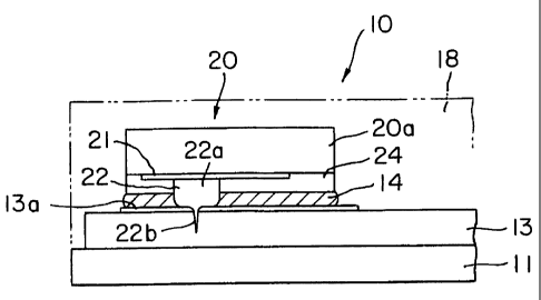
Next, the IC chip 20 will be explained by referring to Figs.
1 and 3. As shown in Figs. 1 and 3, the IC chip 20 has an IC chip
body 20a, a circuit wiring 21 on the bottom of the IC chip body
20a, and a passivation film 24 covering the circuit wiring 21.
Metallic bumps 22 connected to the aluminum antenna coil 13 is
provided on the circuit wiring 21 of the IC chip 20
The IC chip 20 has three bumps 22 (Fig. 4), and a pair of
bumps 22 among them are connected to the antenna coil 13 as a
continuity bump, and the other bump 22 is not connected to the
antenna coil 13 and used as a support bump for supporting the
IC chip 20.
As mentioned above, the pair of continuity bumps and one
support bump, that is, the three bumps 22 in total support the
IC chip 20 on the antenna coil 13, thereby the IC chip 20 can
be supported stably at the three points free of shaky.
The antenna coil 13 is formed in a coil-shape as shown in
Figs. 4(c) and 4(d) and has a pair of ends. The IC chip 20 is
loaded on the antenna coil 13 in a state that a pair of continuity
bumps 22 are connected to the pair of ends of the antenna coil
13 and the IC chip 20 is adhered to the antenna coil 13 as a whole
via an insulating adhesive (nonconductive paste) 14.
Furthermore, the antenna coil 13 and the IC chip 20 are covered
with a protective layer 18 made of resin.
CA 02350705 2001-05-11
4
Each bump 22 has an almost similar shape and as shown in Figs.
2(a) and 2(b), has the base 22a positioned on the side of the
IC chip body 20a and a projection 22b connected to the base 22a
via a shoulder 22c. The projection 22b is held by the base 22a
and piercing in and connected to the antenna coil 13.
Generally, an aluminum oxide film 13a is formed on the surface
of the aluminum antenna coil 13, and the projection 22b of each
bump 22 at least passes through the aluminum oxide film 13a and
is connected to the antenna coil 13. Therefore, the continuity
between the bump 22 and the antenna coil 13 will not be disturbed
by the aluminum oxide film 13a whose continuity is reduced ( Figs .
1 and 3).
In this case, as shown in Figs. 2( a) and 2( b), the projection
22b of the bump 22 is tapered toward its top so as to easily pierce
into the antenna coil 13 and the shoulder 22c is in contact with
the aluminum oxide film 13a of the antenna coil 13. Therefore,
the bump 22 can be fixed onto the aluminum oxide film 13a stably
by the shoulder 22c.
Further, the projection 22b of each bump 22 may be formed
in two stages (Fig. 2(a)) and the bump 22 may be formed in one
stage (Fig. 2(b)).
Such a bump 22 can be formed by pressing a metal wire against
the IC chip body 20a by wire bonding and then pulling up and
breaking the same immediately.
Next, the material and shape of each unit will be explained.
The resin substrate 11 is made of PET and has a thickness of 38
pm. As the substrate 11, in addition to PET, polypropylene ( PP ),
polyethylene, ABS, styrene, polyimide, glass epoxy, PETG,
polycarbonate, paper, PVC, or acrylic resin can be used.
The aluminum antenna coil 13 has a thickness of 30 pm and
the aluminum oxide film 13a generally has a thickness of about
500 A. Therefore, it is desirable that the base 22a of the bump
22 has a height of 10 pm to 100 pm and the projection 22b has
a height of 50 pm to 150 pm.
The insulating adhesive 14 is made from, for example, epoxy,
acrylic resin, cyanoacrate, or urethane.
Next, the manufacturing method of the non-contact data
CA 02350705 2001-05-11
carrier 10 will be explained by referring to Figs. 4(a), (b),
(c), and (d).
Firstly, as shown in Fig. 4(a), the circuit wiring 21, the
bumps 22, and the passivation film 24 are formed on a semiconductor
5 wafer 30. Next, as shown in Fig. 4(b), respective IC chips 20
are separated from the semiconductor wafer 30. On the other hand,
the resin substrate is prepared beforehand and the antenna coil
13 is formed on the resin substrate 11 by the etching method using
a photoresist layer (Fig. 4(c)). In this case, reinforcement
parts 26 and 27 formed of the same material as that of the antenna
coil 13 are installed in the neighborhood of the IC chip 20. The
pair of ends of the antenna coil 13 are respectively arranged
inside and outside the antenna coil 13 on the resin substrate
11, in order to reinforce the strength of the IC chip 20 when
pressing it against the antenna coil 13 and prevent the resin
substrate 11 from contraction.
Next, the insulating adhesive 14 is coated on the pair of
ends of the antenna coil 13 by an adhesive coating machine 31
and the IC chip 20 is loaded on the pair of ends of the antenna
coil 13 with the bumps 22 being directed downward.
Next, as shown in Figs. 4( b) and 6, a compressor 32 is pressed
onto the top of the IC chip 20 and the IC chip 20 is contact-bonded
on the antenna coil 13 by the compressor 32. In this case, the
projection 22b of each bump 22 of the IC chip 20 pierces into
and passes through the aluminum oxide film 13a of the antenna
coil 13 and the shoulder 22c is in contact with the aluminum oxide
film 13a. As a result, the bump 22 can be stably fixed onto the
aluminum oxide film 13a by the shoulder 22c.
After the IC chip 20 is loaded and fixed to the antenna coil
13 in the above manner, the protective layer 18 for covering and
protecting the antenna coil 13 and the IC chip 20 is provided
on the antenna coil 13 and the IC chip 20.
In the embodiment aforementioned, an example that the antenna
coil 13 is directly formed on the resin substrate 11 by the IC
chip is indicated. However, the present invention is not limited
to this manner. As shown in Fig. 5, the antenna coil 13 may be
adhered and installed on the resin substrate 11 via a heat seal
CA 02350705 2001-05-11
6
layer 12. In Fig. 5, the projection 22a of each bump 22 of the
IC chip 20 may pass fully through the antenna coil 12 and reach
the resin substrate 11. When the projection 22a of each bump 22
passes fully through the antenna coil 12, the bump 22 and the
antenna coil 13 can be connected more surely.
Further, an example that the IC chip 20 has three bumps 22
is indicated. However, it may have more than three bumps, for
example, four or five bumps.
As mentioned above, according to the present invention, the
IC chip bumps are connected to the antenna coil by piercing their
projections into the antenna coil, so that even if an oxide film
is formed on the antenna coil surface, the continuity between
the bumps and the antenna coil can be surely realized. Therefore,
a non-contact data carrier which is satisfactorily conductive
and highly precise can be provided.