Note: Descriptions are shown in the official language in which they were submitted.
CA 02351808 2001-06-26
Doc. No. 10-341 CA Patent
A METHOD AND APPARATUS FOR DEMt1LTIPLEXING HIGH BIT RATE
OPTICAL SIGNALS ON A DENSE WAVELENGTH GRID
Field of the Invention
[01] The present invention relates to a method and an apparatus for
demultiplexing
high bit rate optical signals on a dense wavelength grid.
Background of the Invention
[02] In optical communications, wavelength division multiplexing (WDM) is used
for
increasing the transmission capacity of a single optical fibre. The vast
expansion in
demand for communications bandwidth is pushing fibre transmission technology
to its
physical limits. Increased transmission capacity is obtained by increasing the
transmission data rate through the i-ibre. Current transmission data rates are
approaching
the limits of opto-electronic components. Increased transnlission capacity is
also
obtained by reducing the channel frequency spacing in a WDM optical fibre
link. Such
WDM links are referred to as DWI)M (Dense Wavelength Division Multiplexing)
because the density of the wavelength channels per unit wavelength is higher
than in
conventional WDM. The use of both higher data rates and closer channel spacing
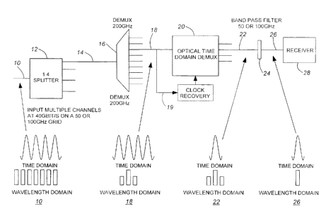
puts
severe demands on the performance of the optical demultiplexer which can limit
the
optical capacity of the transmission link. For example, in current WDM links,
the optical
signals are transmitted at 10 Gbit/s on wavelength channels spaced at
frequency intervals
of 100 GHz. It is planned to increase the data rate to 40 Gbit/s, which
concomitantly
increases the bandwidth of the wavelength channel. The result is that in the
wavelength
domain, the linewidths of adjacent wavelength channels overlap making it
difficult to
demultiplex the individual wavelength channels withotit incurring an
unacceptable loss in
data information.
CA 02351808 2001-06-26
Doc. No. 10-341 CA Patent
[03] To better appreciate the problems consider the following. As the
modulation bit
rate is increased from 10 GHz to 40 CiHz, the bandwidth AB of a channel signal
increases; the relationship between the light pulse width At and signal
bandwidth AB is At
= 1/AB. In the case of a 40 GHz signal using a RZ (return to zero) modulation
format,
the separation between the pulses is 25 ps, but the pulse width, At, is only
12.5ps and
consequently, the modulation bandwidth AB is 80 GHz. The minimum modulated
bandwidth of these signals is 60 GHz. Thus theoretically, wavelength channels
transmitting data at 40 GHz could be multiplexed together onto a DWDM link in
which
the frequency separation is only 100 GHz. However, the theoretical capacity of
the
WDM link is limited by the band pass and the environmental stability of the
optical
filters used in demultiplexing. "I'he available filter pass-band is determined
by the figure
of merit, which is defined as the bandwidth at the 0.5 dB point divided by the
bandwidth
at the 25 dB point and this is typically 0.4 to 0.5. Thus a high quality
optical filter that
could be used to demultiplex the I)WDM signals have a measured pass bandwidth
of 50
GHz and net bandwidth of only 25 GHz. Misaligtunent of the filter wavelength
to the
signal wavelengths due to manufacturing tolerances and environmental factors
such as
ageing will reduce the available bandwidth even further. Thus, demultiplexing
this
optical signal using prior art techniques would result in unacceptable error
rates and data
loss.
[04] It is an object of the invention to provide a deinultiplexer capable of
demultiplexing high bit-rate optical signals.
[05] It is a further object of the invention to provide a demultiplexer
capable of
2f, demultiplexing optical signals in which the linewidths of adjacent
channels overlap in the
wavelength domain.
[06] It is a further object of the invention to provide a low loss high bit-
rate
demultiplexer.
2
CA 02351808 2001-06-26
Doc. No. 10-341 CA Patent
[07] It is another object of the invention to provide a high bit-rate
demultiplexer
having a low error rate.
`> Summary of the Invention
[08] In accordance with the invention there is provided an optical
demultiplexer for
demultiplexing an optical signal having a pluralityo of channels at a
predetermined
channel spacing comprising demultiplexing means having a frequency spacing
larger
than the predetermined channel spacing for receiving the optical signal and
for dividing
the optical signal by wavelength into a plurality of wavelength streams
broader than the
predetermined channel spacing, time domain demultiplexing means for receiving
one of
the plurality of wavelength streams and for dividing the one of the plurality
of
wavelength streams into a plurality of time domain demultiplexed wavelength
streams,
and optical filtering means for dernultiplexing one of the plurality of time
domain
demultiplexed wavelength streams into a single channel.
[09] In accordance with an embodiment of the invention the optical
demultiplexer
further comprises splitting means for splittirig the optical signal into at
least two sub-
signals before launching one of the sub-signals into the demultiplexing means.
[10] In accordance with another embodiment of the present invention the
optical
demultiplexer further comprises cilock recovery means for obtaining a clock
signal from
the one of the plurality of wavelength streanis and for providing the clock
signal to the
2_41 time domain demultiplexing meanis for dividing the one of the plurality
of wavelength
streams into a plurality of time dovnain demultiplexed wavelength streams in
dependence
upon the clock signal.
[11] The invention further provides an optical demultiplexer for
demultiplexing a
multiplexed N channel optical signal comprising splitting means for splitting
the
multiplexed N channel optical signal into a plurality of multiplexed N channel
optical
3
CA 02351808 2001-06-26
Doc. No. 10-341 CA Patent
sub-signals, first demultiplexing rneans for coarse wavelength demultiplexing
the
plurality of multiplexed N channel optical sub-signals into M sub-signals,
second
demultiplexing means for time demultiplexing the M sub-signals into R sub-
signals, and
third demultiplexing means for wavelength demultiplexing the R sub-signals
into N
;i single channels.
[12] In accordance with an embodiment of the invention M is a smaller number
than
N.
[13] In accordance with a further embodiment of the invention, the plurality
of
multiplexed N channel optical sub-signals and the M sub-signals have a data
rate B. The
R sub-signals have a data rate C which is a lower than data rate B. Data rate
B is equal to
the sum of the data rates C of all the R sub-signals of one of the plurality
of multiplexed
N channel optical sub-signals or the M sub-signals.
1141 In accordance with another aspect of the invention there is provided a
method for
demultiplexing a high bit-rate sigrial on a dense optical grid comprising the
steps of
providing the high bit-rate signal including a plurality of wavelength
channels at a
predetermined channel spacing to a coarse wavelength demultiplexer, performing
a
coarse wavelength demultiplexing for dividing the high bit-rate signal into
wavelength
streams broader than the predetermined channel spacing, performing an optical
time
domain demultiplexing for dividir.tg at least one of the wavelength streams
into a plurality
of time demultiplexed streams, and filtering at least one time dernultiplexed
stream
through a wavelength filter for obtaining at least one individual wavelength
channel.
[15] The present invention has developed a method and an apparatus for
demultiplexing very high bit rate signals which are multiplexed at close
channel spacing.
The invention has found that a dernultiplexing method combining time and
wavelength
demultiplexing can be achieved within the practical limits of optical and
electronic
technology.
4
CA 02351808 2001-06-26
Doc. No. 10-341 CA Patent
[16] In accordance with the present invention there is provided a method for
demultiplexing a high bit rate sigrial comprising a first coarse optical
frequency
demultiplexing step for separating; signals of groups of channels, followed by
a
subsequent time domain demultiplexing step for providing sufficient signal
separation
within each group of channels to perform a third optical frequency domain
demultiplexing step separating indlividual channel signals.
[17] A preferred method in accordance with the present invention comprises a
method
for demultiplexing a high bit rate signal on a dense optical grid comprising
the steps of :
providing a signal including a plurality of wavelength channels having a
predetermined channel spacing;
performing a coarse wavelength demultiplexing of wavelength streams broader
than the predetermined channel spacing;
identifying a timing signal from the wavelength streams;
performing an optical time domain demultiplexing for at least one of the
wavelength streams with respect to the timing signal;
filtering the at least one time deniultiplexed stream through a filter to
obtain an
output signals having the predetermined channel spacing.
[18] The method is further improved by initially splitting the signal into at
least two
streams and providing each stream into a separate coarse wavelength
demultiplexer of
different but overlapping wavelerigth ranges.
Brief Description of the Drawings
[19] Exemplary embodiments of the invention will now be described in
conjunction
with the drawings in which:
[20] Fig. 1 a is a flow chart to surnmarize the invention of demultiplexing a
high bit-
rate optical signal by triple stage dernultiplexing;
[21] Fig. 1 is a schematic illustration of the invention shown in an exemplary
scale;
5
CA 02351808 2001-06-26
Doc. No. 10-341 CA Patent
[22] Fig. 2 is a graph illustrating exemplary signals at 40 Gbits/s and a
filter response
(for demonstration only) of intensity versus wavelength following a first
wavelength
demultiplexing step;
[23] Fig. 3 is a graph illustrating exenlplary signals at 40 Gbits/s of
intensity versus
time;
[24] Fig. 4 is a graph illustrating the signal of Fig. 3 following the time
domain
demultiplexing step; and,
[25] Fig. 5 is a graph illustrating the signal and the filter response of Fig.
2 following a
final wavelength demultiplexing step.
Detailed Description of Preferred Embodiments
[26] Reference is now made to Fig. 1 a presenting a flow chart to summarize
the
invention of demultiplexing a high bit-rate optical signal by demultiplexing
in three
stages. The first and the third stage are optical frequency domain
demultiplexers and the
second stage is an optical time domain demultiplexer. A multiplexed signal 1
having a
plurality of wavelength channels k I to a, õ is split into a number of data
streams and each
one is launched into a coarse wavelength demultiplexer 2. The number of data
streanls
required depends on the ratio of the frequency spacing of the coarse
demultiplexer to the
frequency spacing of the high bit-rate optical signal. The frequency spacing
of the
demultiplexer can be an integer or non-integer multiple of the channel
spacing, but
advantageously, the frequency spacing is some integral number i.e. twice the
channel
spacing of the high bit-rate signal. Furthermore, conveniently, the channel
spacing has
frequency spacing according to a standardized International Telecommunications
Union
(ITU) frequency grid and the demultiplexer demultiplexes the optical signal
according to
the standardized ITU frequency grid. In this first stage of the
demultiplexing, only those
wavelength channels at the coarse demultiplexer frequency spacing are selected
and
demultiplexed from the input optical signal. The wavelength channels that lie
in between
the coarse demultiplexer frequency spacing at=e recovered by demultiplexing
the other
data streams obtained by splitting thie input signal befor=e entering the
coarse
6
CA 02351808 2001-06-26
Doc. No. 10-341 CA Patent
demultiplexer 2. The coarse wavelength demultiplexer 2 also has a
demultiplexing
bandwidth that is larger than the frequency spacing of the optical signal.
This is
necessary so that a bandwidth of the 40 GHz signal is not reduced in the
demultiplexing
process and all the information in the signal is retained. As a result, the
signal outputs
:i from the coarse wavelength demultiplexer 2 are not purely one wavelength
channel, but a
demultiplexed light output contains significant aniounts of the light from
adjacent
wavelength channels on either side of the demultiplexed channel. Each
wavelength
channel output from the coarse demultiplexer 2 is then passed through an
optical time
domain demultiplexer 3 which divides the high bit-rate wavelength streams into
a number
of time domain demultiplexed streams having lower bit-rates (sub-bit-rates).
The
wavelength streams can be divided into any number of sub-bit-rates, however,
the sum of
the sub-bit-rates is equal to the bit-rate of the wavelength stream send into
the time
domain demultiplexer 3. The signal output from the time domain demultiplexer
still
contains light at the channel wavelength and the adjacent channels, however,
the process
of time domain demultiplexing has reduced the bit rate so that the data
information is
contained in a smaller bandwidth. The time domain demultiplexed streams can
now be
passed through a narrow band wavelength filter 4 having a linewidth that is
narrower than
the frequency spacing between the channels of the high bit rate optical signal
but
sufficiently broad to capture all the data infoimation. In this way the
wavelength-time
domain demultiplexer demultiplexes the high bit rate DWDM optical signal into
its
separate individual wavelength channels k i to k n, as denoted by reference
numeral 5, with
each wavelength channel comprising several lower bit rate channels.
[27] A demultiplexer in accordance with the present invention is shown
schematically
2`> in Fig. 1. At 10 a signal of multiple wavelength channels at 40 Gbits/s
spaced on a 50
GHz or 100 GHz optical network grid is divided by a 1:4 splitter 12 in the
case of a 50
GHz channel spacing or a 1:2 splitter in the case of a 100 GHz channel
spacing. As
shown in Figure 2, the linewidths of the individual wavelength channels of the
optical
signal overlap adjacent channels iin the wavelength domain due to a high
modulation rate
of the optical signals. Figure 3 shows the 40 Gbit/s signal in the time
domain; the optical
pulses are spaced at 25 ps intervals and have a pulse width of 12.5 ps for a
return-to-zero
7
CA 02351808 2001-06-26
Doce No, 10-341 CA Patent
(RZ) modulation format. In the following description of this embodiment of the
invention, the channel spacing of the input signal 10 is taken as 100 GHz. An
output
signal 14 from the splitter 12 (1:2 in this case) is routed to a 200 GHz
coarse wavelength
demultiplexer 16. The coarse wavelength demultiplexer 16 demultiplexes every
second
wavelength channel from the optical signal input thereby producing at the
outputs of'the
demultiplexer a sequence of wavelength channels spaced by 200 GHz. A typical
200
GHz demultiplexer has a measured bandwidth of 120 GHz and a net bandwidth of
80
GHz. Figure 2 shows the bandwidth of a typical filter in comparison to the
linewidths of
the wavelength channels. Since the bandwidth of the demultiplexer 16
approaches the
100 GHz channel spacing of the optical signal 10, each wavelength channel at
the output
of the demultiplexer 16 contains light not only at the channel wavelength but
also light
from the adjacent channels spaced at 100 GHz on either side. In the wavelength
domain,
the output from the coarse wavelength demultiplexer 16 appears as a single
wavelength at
demultiplexed channel wavelength with smaller sidebands at wavelengths 100 GHz
on
either side of the channel wavelength. It is estimated that the 200 GHz
demultiplexer
attenuates the adjacent channels by only 5 to 10 dB which is insufficient
isolation for the
data to be detected with a low error rate.
[28] Since the coarse wavelength demultiplexer 16 provides only one half of
the
wavelength channels contained in the input WDM optical signal 10, a second
coarse
wavelength demultiplexer, not shown in Fig. 1, connected to the other output
from the
optical splitter 12 is used to provide the wavelength channels located in
between the
channel frequencies of the coarse wavelength demultiplexer.
[29] Each output signal 18 from the coarse wavelength demultiplexer 16 is
routed to
an optical time domain demultiplexer 20. Figure 3 shows the optical signal in
the time
domain before entering the optical time domain demultiplexer. A number of
technologies exist for realizing the optical time domain demultiplexer
function, such as
LiNbO3 modulators and semiconductor optical amplifier switches. Before
entering the
time domain demultiplexer 20, a portion of the signal 18 is tapped off in
order to provide
a means to recover the clock frequency 19 for the 40 Gbit/s signal. Although
the signal-
8
CA 02351808 2001-06-26
Doc. No. 10-341 CA Patent
to-noise ratio in the tapped light signal is too low to permit an error free
recovery of the
data, it is sufficiently high to permit the recovery of the clock frequency,
which is used to
trigger the optical time domain demultiplexer 20. The time domain
demultiplexer 20
demultiplexes the input signal or wavelength strearn 18 into several time
domain
`> demultiplexed wavelength streams having a lower bit-rate than the input
wavelength
stream 18. The sum of the bit-rates of these lower bit rate channels equals
the bit-rate of
the input data stream 18 to the time domain demultiplexer 20. For example, the
40 Gbit/s
data stream shown in Fig. 3 is deniultiplexed into four 10 Gbit/s data
streams, i.e. the
time domain demultiplexed wavelength streams. One of these lower bit-rate 10
Gbit/s
data streams is shown in Fig. 4; the pulse width is still 12.5 ps, but the
pulse separation is
now 100 ps. In the wavelength domain, the bandwidth of one of'these 10 GHz
data
streams still has a 80 GHz bandwidth at the channel wavelength and residual
side bands
spaced at 100 GHz on either side of the channel wavelength. However, because
the data
rate is now onlyl0 Gbit/s (RZ sigrial bandwidth 20 GHz) as compared to 40
Gbit/s data
rate (RZ signal bandwidth 80 GHz), the adjacent channels can be removed using
a
narrow band filter 24 without losing any data. Therefore the output signal 22
from the
optical time domain demultiplexer 20 is passed through a narrow band optical
band pass
filter 24 having a bandwidth sufficiently small to remove the optical signal
in the adjacent
channels. This filtering action is illustrated in Fig. 5. The demultiplexed
signal 26 from
each filter 24 passes to a receiver 28 where the data is recovered without any
loss of
information.
9