Note: Descriptions are shown in the official language in which they were submitted.
CA 02352062 2001-05-28
WO 00/36666 PCT/US99/29789
METHOD FOR PRINTING OF TRANSISTOR
ARRAYS ON PLASTIC SUBSTRATES
Related Applications
This invention claims priority to provisional application U.S.S.N. 60/112,330
filed on
December 15, 1998 and is a continuation-in-part of utility application
U.S.S.N. 09/289,036 filed
on April 9, 1999, the entire disclosure of each application is incorporated
herein by reference.
Field of ~he Invention
This invention generally relates to methods of manufacturing electronic
devices, and
more specifically to methods of manufacturing non-linear devices for
addressing electronic
displays.
Background of the Invention
Microencapsulated, particle-based displays can be made highly reflective,
bistable, and
optically and electrically efficient. To obtain a high resolution display,
however, individual
pixels of a display must be addressable without interference from adjacent
pixels. One way to
achieve this objective is to provide an array of nonlinear elements, such as
transistors, diodes, or
varistors, where one or more nonlinear elements are associated with each
pixel.
Most examples of nonlinear elements to date have been fabricated using vacuum-
deposited silicon on glass. This process is costly in addition to being
complex. The complexity
prevents large area devices from being readily constructed. In addition; it is
difficult to create
silicon transistors on plastic or other flexible film.
CA 02352062 2001-05-28
WO 00/36666 PCTNS99/29789
-2-
Recently, there has been significant development in the area of organic
semiconducting
polymers and molecules. Thin film transistors have been made out of
semiconducting polymers.
See Bao et al., Soluble and Processable Regioregular Poly(3-hexylthiophene)
for Thin Film
Field Effector Transistor Applications with High Mobility, Appl. Phys. Lett.
69(26), 4108
(December 1996); and Bao et al., High-Performance Plastic Transistors
Fabricated by Printing
Techniques, Chem. Mater. 1997, 9, 1299. U.S. Patent No. 5,574,291 describes
addressing liquid
crystal displays with transistors made out of semiconducting polymers. While
remarkable
advances have been made in the performance of organic-based transistors, the
mobility
characteristics of many organic semiconductor materials and devices are
insufficient to
successfully drive many types of liquid crystal or emissive displays.
Therefore, many organic-
based transistors are not suitable for use with liquid crystal displays.
In addition, liquid crystals can degrade the transistors when they come in
contact with the
transistors. Many organic semiconductor materials can be swollen by, or
dissolved by, liquid
crystalline fluids because those fluids are good solvents. This solvent
compatibility makes it
challenging to design systems in which organic transistor devices can remain
stable while in
contact with or close proximity to liquid crystalline solvents, limiting their
viability.
Many organic-based transistors have been made using a screen printing
technology, in
which the organic material is squeezed through an opening in a mesh to produce
fine lines.
Lines having a pitch as small as about 250 microns have been printed using the
screen printing
technology. While this line spacing is adequate for some applications, it is
preferable to
construct transistors with much smaller features, a goal not readily reached
using screen printing.
CA 02352062 2001-05-28
WO 00/36666 PCT/US99/29789
-3-
In addition, the solvent carrier used for supporting screen printable
materials must have a
certain range of viscosity and surface energy characteristics. Such solvent
carriers can
potentially interfere with the electrical characteristics of the semiconductor
material of the
transistors. Finding proper solvent carriers, therefore, is difficult.
Summary of the Invention
The invention relates to a method of manufacturing an electronic device. In
one aspect,
an electronic device is manufactured in accordance with the following steps.
An ink jet printing
system is provided. The ink jet printing system includes a print head and a
transfer member. A
substrate is provided. A plurality of ink drops are dispensed from the print
head to a surface of
the transfer member forming an ink pattern corresponding to at least a
component of the
electronic device. The plurality of ink drops can include a conductive
material and/or a
semiconductive material. The ink pattern is transferred from the transfer
member to the
substrate, thereby forming the component of the electronic device.
In one embodiment, the ink drops include an organic conductive material and/or
an
organic semiconductive material. In another embodiment, the ink drops include
a colloidal
inorganic conductive material and/or a colloidal inorganic semiconductive
material, or
organometallic material. In one embodiment, the ink drops further includes an
insulating
material.
In one embodiment, the ink drops form an ink pattern corresponding to at least
a
component of a transistor, such as a source electrode, a drain electrode, a
dielectric layer, a
semiconductor layer, or a gate electrode.
CA 02352062 2001-05-28
WO 00/36666 PCT/US99/29789
-4-
In one embodiment, the ink jet printing system further includes an applicator
for applying
a release material to the transfer member. For example, the release material
can be applied to a
surface of the transfer member and the plurality of ink drops can be dispensed
adjacent the
release material.
In one embodiment, the substrate is provided between the transfer member and a
pressure
applying member. The substrate can be provided on a conveyor belt.
Alternatively, a plurality
of substrates can be provided for a batch process. The substrate can be
flexible.
In one embodiment, an electronic display media is provided and assembled with
the
electronic device. The electronic display media can include a plurality of
microcapsules, where
each capsule includes particles dispersed in a fluid. Alternatively, each
microcapsule can include
a bichromal sphere.
Brief Description of the Drawings
The foregoing and other objects, features and advantages of the present
invention, as well
as the invention itself, will be more fully understood from the following
description of preferred
1 S embodiments, when read together with the accompanying drawings, in which:
Figure 1 a shows a cross-section view of a transistor according to one
embodiment of the
present invention.
Figure lb shows a cross-section view of a transistor according to one
embodiment of the
present invention.
Figure 2 shows a cross-section view of a diode according to one embodiment of
the
present invention.
CA 02352062 2001-05-28
WO 00/36666 PCT/US99/29789
-5-
Figure 3 illustrates ink jet printing according to one embodiment of the
present invention.
Figure 4 illustrates ink jet printing according to one embodiment of the
present invention.
Figure 5 illustrates ink jet printing using a transfer member according to one
embodiment
of the present invention.
Figure 6 illustrates ink jet printing using a transfer member according to one
embodiment
of the present invention.
Figure 7a shows a cross-section view of an electronic display according to one
embodiment of the present invention.
Figure 7b shows a cross-section view of an electronic display according to one
embodiment of the present invention.
Figure 7c shows a top view of the electronic display of Figure7b with the
display media
and the first electrode removed.
Figure 8 shows a cross-section view of a transistor according to one
embodiment of the
present invention.
Figure 9 shows a cross-section view of an electronic display according to one
embodiment of the present invention.
Figure 10 shows a cross-section view of an electronic display according to one
embodiment of the present invention.
Figure 11 a shows a partial cross-section view of an electronic ink according
to one
embodiment of the present invention.
CA 02352062 2001-05-28
WO 00/36666 PCT/US99/29~89
-6-
Figure 11 b shows a partial cross-section view of an electronic ink according
to one
embodiment of the present invention.
Figure 11 c shows a partial cross-section view of an electronic ink according
to one
embodiment of the present invention.
Figure 11 d shows a cross-section view of an electronic ink according to one
embodiment
of the present invention.
Figure 12 illustrates a method of assembling an electronic display according
to one
embodiment.
Detailed Description of Preferred Embodiments
Referring to Figure 1 a, an organic-based field effect transistor 10 includes
a substrate 12,
a gate electrode 14 provided on the substrate 12, a dielectric layer 16
provided on the gate
electrode 14, an organic semiconductor 18 provided on the dielectric layer 16,
and a source
electrode 20 and a drain electrode 22 provided on the organic semiconductor
18.
The substrate 12 can be flexible. For example, the substrate 12 can be made of
an
insulating polymer, such as polyethylene terephthalate (PET), polyester,
polyethersulphone
(PES), polyimide film (e.g. Kapton, available from Dupont [Wilminton, DE];
Upilex available
from Ube Corporation [Japan]), or polycarbonate. Alternatively, the substrate
12 can be made of
an insulator such as undoped silicon, glass, or other plastic material. The
substrate 12 can also
be patterned to serve as an electrode. The substrate 12 can further be a metal
foil insulated from
the gate electrode 14 by a non-conducting material. The substrate 12 can also
be a woven
material or paper, planarized or otherwise modified on at least one surface by
a polymeric or
other coating to accept the other structures.
CA 02352062 2001-05-28
WO 00!36666 PCTNS99/29789
_ '7 _
The gate electrode 14, the source electrode 20, and the drain electrode 22,
for example,
can comprise a metal such as aluminum or gold. The electrodes 14, 20, 22 can
also comprise a
conductive polymer such as polythiophene or polyaniline. The electrodes 14,
20, 22 can further
include a printed conductor such as a polymer film comprising metal particles
such as silver or
nickel, a printed conductor comprising a polymer film containing graphite or
some other
conductive carbon material, or a conductive oxide such as tin oxide or indium
tin oxide.
The dielectric layer 16, for example, can comprise a silicon dioxide layer.
Alternatively,
the dielectric layer 36 can comprise an insulating polymer such as polyimide
and its derivatives,
poly-vinyl phenol, polymethylmethacrylate, polyvinyldenedifluoride, an
inorganic oxide such as
metal oxide, an inorganic nitride such as silicon nitride, or an
inorganic/organic composite
material such as an organic-substituted silicon oxide, or a sol-gel
organosilicon glass. The
dielectric layer 36 can also comprise a bicylcobutene derivative (BCB)
available from Dow
Chemical (Midland, MI), spin-on glass, or dispersions of dielectric colloid
materials in a binder
or solvent.
The semiconductor layer 18 can be an organic polymer. In one embodiment, the
organic
semiconductor comprises a polymeric or oligomeric semiconductor. Examples of
suitable
polymeric semiconductors include, but are not limited to, polythiophene,
poly(3-
alkyl)thiophenes, alkyl-substituted oligothiophene, polythienylenevinylene,
poly(para-
phenylenevinylene) and doped versions of these polymers. An example of
suitable oligomeric
semiconductor is alpha-hexathienylene. Horowitz, Organic Field Effect
Transistors, Adv.
Mater., 10, No. 5, p. 365 (1998) describes the use of unsubstituted and alkyl-
substituted
oligothiophenes in transistors. A field effect transistor made with
regioregular poly(3-
hexylthiophene) as the semiconductor layer is described in Bao et al., Soluble
and Processable
CA 02352062 2001-05-28
WO 00/36666 PCTNS99/29789
_g_
Regioregular Poly(3-hexylthiophene) for Thin Film Field Effect Transistor
Applications with
High Mobility, Appl. Phys. Lett. 69 (26), p. 4108 (December 1996). A field
effect transistor
made with a-hexathienylene is described in U.S. Patent No. 5,659,181.
In another embodiment, the organic semiconductor 18 comprises a carbon-based
compound. Examples of suitable carbon-based compounds include, but are not
limited to,
pentacene, phthalocyanine, benzodithiophene, buckminsterfullerene or other
fullerene
derivatives, tetracyanonaphthoquinone, and tetrakisimethylanimoethylene. The
materials
provided above for forming the substrate, the dielectric layer, the
electrodes, or the
semiconductor layer are exemplary only. Other suitable materials known to
those skilled in the
art having properties similar to those described above can be used in
accordance with the present
invention.
Referring to Figure lb, an organic-based field effect transistor 30 includes a
substrate 32,
a gate electrode 34 disposed adjacent the substrate 32, a dielectric layer 36
disposed adjacent the
gate electrode 34, an organic semiconductor 38 disposed adjacent the
dielectric layer 36, and a
source electrode 40 and a drain electrode 42 disposed adjacent the dielectric
layer 36 and in
contact with the semiconductor layer 38.
The field effect transistor configurations provided in Figures la and lb are
exemplary
only. Other transistor designs known to those skilled in the art can be used
in accordance with
the present invention. For example, a top gate structure in which the source
and drain electrodes
are placed adjacent the substrate, covered by the semiconductor layer, which
in turn is covered
by the dielectric and gate electrode, can also be used in accordance with the
present invention.
CA 02352062 2001-05-28
WO 00/36666 PCTNS99/29789
-9-
Back-to-back diodes may also be used as a non-linear element in an electronic
display.
Referring to Figure 2, a back-to-back organic-based diode 50 includes a
substrate 51, a patterned
stack of a first conductive layer 52 provided on the substrate 51, a layer 54
of p-type
semiconducting material provided on the first conductive layer 52, a layer of
n-type 56
semiconducting material provided on the p-type semiconducting layer 54, a
second layer of p-
type semiconducting material 54' provided on the n-type semiconducting layer
56, and a second
conductive layer 58 provided adjacent the second p-type semiconducting layer
54'. In another
embodiment, the back-to-back diode is formed by depositing a stack consisting
of a first
conducting layer, a semiconducting layer, a second conducting layer
characterized by a different
work function than the first conducting layer, a second semiconducting layer,
and a third
conducting layer with the same work function as the first conducting layer.
For example, gold
and aluminum are known to have markedly different work functions and thus can
be used as the
first conducting layer and the second conducting layer. The diode
configuration provided in
Figure 2 is exemplary only.
The substrate 51 can be flexible and be made of various materials discussed
above in
connection with Figure l a, and the conductors 52, 58 can be made of various
materials such as
conductive polymers or dispersions of conductive particles as discussed above.
The
semiconducting layers can be made from the organic semiconductors discussed
above. Both n-
type and p-type organic semiconductors are known to those skilled in the art.
Other diode
designs known to those skilled in the art can be implemented using the present
invention.
According to the present invention, one or more constituent layers of non-
linear
electronic devices such as the transistors of Figures 1 a and 1 b and the
diode of Figure 2 can be
manufactured by ink jet printing.
CA 02352062 2001-05-28
WO 00/36666 PCT/US99/29789
-10-
Refernng to Figure 3, an ink jet printer 60 includes a print head 62 coupled
to a control
assembly (not shown). In one embodiment, the print head 62 includes a
plurality of orifices for
dispensing one or more fluids onto a desired media. For example, one sub-group
of orifices can
be connected to a reservoir that contains a conducting fluid solution, a
second sub-group of
orifices can be connected to a reservoir that contains a semiconducting fluid
solution, and a third
sub-group of orifices can be connected to a reservoir that contains an
insulating fluid solution.
In one embodiment, the print head 62 can further include a fourth group of
orifices
connected to a reservoir that contains a solution comprising a precursor
material. The precursor
material advantageously affects subsequent deposition of the semiconducting
material. The
precursor material can be selected from a wide spectrum of available materials
including, but not
limited to, surface active agents such as octadecyltrichlorosilane (OTS). By
modifying the
dielectric surface chemistry, the surface active agents can improve the
performance of a
completed thin film transistors.
In another embodiment, a plurality of print heads, each capable of printing
only one
constituent material, can be used to deposit each of the materials used to
build electronic devices.
In operation, the control assembly applies the necessary control signals to
each of the
orifices to control the sequence of printing of the various ink materials. The
ink drops 61 are
dispensed on the substrate 63 through the openings in the print head 62. The
print head 62
preferably uses a pulse-on-demand method, and can employ one of the following
methods to
dispense the ink drops 61: piezoelectric, magnetostrictive, electro-
mechanical, electropneumatic,
electrostatic, rapid ink heating, magnetohydrodynamic, or any other technique
well known to
those skilled in the art. The ink drops 61 dispersed on the substrate 61 form
an ink pattern which
CA 02352062 2001-05-28
WO 00/36666 PCTNS99/Z9789
-11-
corresponds to a constituent layer of an electronic device. The ink patterns
undergo a curing step
or another processing step before subsequent layers are applied.
Referring to Figure 4, the substrate 63 can be provided on a transport 64
which includes a
stage 65 and a pair of rollers 66. The rollers 66 provide continuous movement
of the substrate 63
relative to the print head 62 resulting in a continuous printing process.
Alternatively, multiple
substrates can be processed as a batch.
In one embodiment, an electronic device can be manufactured using an ink jet
printer of
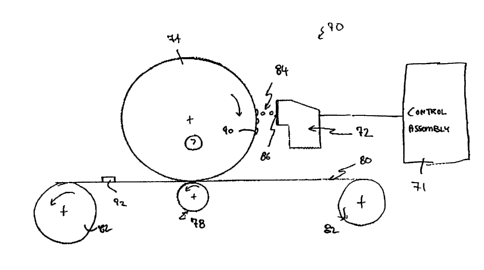
Figure 5. The ink jet printer 70 includes a control assembly 71, a print head
72, a transfer
member 74, a tensioner 78, and a transport 82. The control assembly 71
includes sufficient
driving electronics to allow for independent control of the dispensing of
fluid drops from each of
the orifices. The control assembly also regulates the speed at which the
transfer member 74 and
substrates 80 move through the printer 70.
The transfer member 74 can be a drum. Alternatively, the transfer member 74
can have
another configuration sufficient for receiving ink drops to form an ink
pattern and for transfernng
the ink pattern to a substrate 80. The transfer member 74 can include surface
material which aids
transfer of the ink pattern to the substrate 80. For example, the transfer
member 74 can be coated
with a thin film of an oil-based material to facilitate the transfer of
aqueous-based ink drops from
the surface of the transfer member 74. In one embodiment, the transfer member
74 is constructed
of a rigid body and a surface material comprising a resilient polymeric
material. In another
embodiment, the surface of the transfer member 74 can be coated with a non-
sticking layer such
as silicone, silicone rubber or teflon. In one example, the transfer member 74
is made of an
aluminum base material and a surface layer is made from silicon rubber doped
with carbon filler
CA 02352062 2001-05-28
WO 00/36666 PCT/US99/29789
-12-
to prevent charge accumulation. The transfer member 74 can be rigid or
flexible. The transfer
member 74 can also be made of a woven material. The material for the transfer
member 74 can
be chosen on the basis of several parameters, including precision of transfer,
mechanical
properties, surface properties, durability, and cost.
The tensioner 76 can be a backing roller which, together with the transfer
member 74,
provides pressure to the substrate 80. Alternatively, the tensioner 76 can
have another
configuration sufficient to support and provide pressure to the substrate 80.
Alternatively, other
means of transporting the substrate 80 relative to the transfer member 74
and/or providing
pressure to the substrate 80 can be used in accordance with the present
invention. The transport
I O 82 can include a pair of rollers as shown in Figure 5.
In one embodiment, the ink jet printer 100 further includes a planzarizer for
planzarizing
the ink pattern provided on the substrate 80.
In operation, a substrate 80 is provided between the transfer member 74 and
the tensioner
78. The substrate 80 is delivered to the transfer member 74 through the
rollers 82, which
15 continuously move the substrate 80 relative to the transfer member 74.
The control assembly 71 provides appropriate control commands (e.g. voltages)
to the
print head 72 to cause the print head 72 to dispense droplets of ink. The
control assembly 71
produces an independent output signal for each orifice 86 on the print head
72. The signal
waveform is selected based upon the print head design, and upon the fluid
mechanical properties
20 (e.g. density, viscosity, surface tension) of the ink material. The control
assembly also
synchronizes the advance speed of the transfer member 74 or the substrate 80
with the print rate.
CA 02352062 2001-05-28
WO 00/36666 PCT/US99/29789
-13-
The print head 72 dispenses ink drops 84 on a surface of the transfer member
74 through
the orifices 86. The ink drops 84 can include a semiconductor material, a
conductor material
and/or an insulator material to form an electronic device. The ink drops can
be organic material
based or colloidal inorganic material based. The ink drops 84 form an ink
pattern 90, which
corresponds to a portion of the electronic device, on the surface of the
transfer member 74. The
transfer member 74 rotates relative to the substrate 80 until the portion of
the transfer member 74
having the ink pattern 90 comes in contact with the substrate 80. The ink
pattern is transferred
from the transfer member 74 to the substrate 80 as the transfer member 74
contacts the
substrate 80. The ink pattern transferred to the substrate 80 can subsequently
be cooled, cured,
or treated further to convert the ink material into a component of the
electronic device. These
steps are repeated until all the necessary components of an electronic device
are printed on the
substrate 80. Thereafter, electronic device 92 is formed on the substrate 80.
For some ink
materials, it is preferable to cure the ink material after deposition on the
transfer member 74, but
before transferring it to the substrate 80.
Alternatively, electronic devices can be manufactured using the ink jet
printer 100 of
Figure 6. The ink jet printer 100 of Figure 6 is substantially similar to the
ink jet printer 70 of
Figure 5. In addition to the features of the ink jet printer 70 of Figure 5,
the ink jet printer 100
further includes a release agent applicator 102, a blade 106, and a stripper
104.
The release agent applicator 102 can be a squeegee roller which rotates in the
direction
opposite that of the transfer member 74. The squeegee roller, along with the
blade 106, provide a
controlled thin coating of a release agent to be provided on a surface of the
transfer member 74
prior to dispensing the ink drops on the transfer member 74. The release agent
aids transfer of
the ink pattern 90 to the substrate 80. The desirable properties of the
release agent depend
CA 02352062 2001-05-28
WO 00/36666 PCTNS99/29789
- 14-
intimately upon the chemistry of the material in the ink drops. It is
desirable for the release agent
to have the following properties: ( 1 ) the ink material should be insoluble
in the release agent; (2)
the difference between the surface tension of the release agent and the
surface tension of the ink
material should be such that a contact angle of the at-rest ink drop is less
than 90 degrees; (3) the
ink drop should be transferred to a substrate without leaving any significant
residue on the
surface of the transfer member.
The ink jet printers provided in Figures 5 and 6 are exemplary only. Ink jet
printers
having other variations known to those skilled in the art can also be used in
accordance with the
present invention.
The ink jet printer which uses the transfer member improves the quality of
printing,
making the printed image more precise. For example, it reduces blurring of the
printed image
which results from the wicking of the ink into the substrate due to the flow
of the liquid based
ink. Also, the transfer member's surface may be of much higher quality
(smaller surface
roughness and more carefully controlled surface chemistry) than that of the
substrate. Therefore,
the ink pattern transferring from the transfer member to the substrate can be
more precise.
According to the present invention, small drops of conductor or semiconductor
can be deposited
in precise locations on a substrate to create fine lines having width smaller
than 50 microns, with
precisely controlled spaces between the lines.
Using this technique, one or more non-linear devices can be fabricated. For
example, a
transistor can be constructed as follows. First, a conductive ink solution is
deposited in the
desired pattern onto the transfer member, transferred to a substrate, and
cured or further
processed to form a transistor gate. Second, an insulating ink solution is
deposited in the desired
CA 02352062 2001-05-28
WO 00/36666 PCTNS99/29789
-IS-
pattern onto the transfer member, transferred to the substrate adjacent the
transistor gate, and
cured or further processed to form the gate dielectric. Third, a
semiconducting ink solution is
deposited in the desired pattern onto the transfer member, transferred to the
substrate adjacent the
gate dielectric, and cured to form the semiconducting thin film. Finally, the
conductive ink
solution is again applied in the desired pattern onto the transfer member,
transferred to the
substrate adjacent the semiconducting thin film, and cured or further
processed to form the
source and drain structures. This technique may be used to create any of a
wide number of thin
film transistor structures known to those skilled in the art. Means of curing
printed materials to
make them solvent resistant are well known to those skilled in the art. Such
curing methods
include, but are not limited to, heating, photochemical reaction, and solvent
evaporation. Diodes
and other electronic devices can be manufactured through ink jet printing in a
manner similar to
that described with respect to a transistor.
The transistors and other electronic devices made in accordance with the
present
invention and as described above can be used in addressing an electronic
display. Referring to
Figure 7a, an electronic display 110 includes a display media 112, a first
electrode 1 I6, a second
electrode 118, an array of transistors 120, an array of row electrodes 117,
and an array of column
electrodes 115. The first electrode 116 is disposed on a first surface I 11 of
the display media
112. In one embodiment, the first electrode 116 comprises a transparent,
continuous electrode.
The second electrode 118 disposed on a second surface 113 of the display media
112 comprises
an array of patterned pixel electrodes 118. Each patterned electrode 118
defines a pixel of the
display 110. The transistors I20 are located underneath the pixel electrodes
118. Each transistor
120 is electrically connected to a pixel electrode 118 to address a pixel. A
row electrode 117 is
CA 02352062 2001-05-28
WO 00/36666 PCTNS99/29789
-16-
electrically connected to all the transistors 120 in that row. A column
electrode 115 is
electrically connected to all the transistors 120 in that column.
In the display 110 of Figure 7a, the transistors 120 are located on the
backside of the
display 110 from the standpoint of the viewer 119. Alternatively, the
transistors 120 can be
located on the front side of the display 110. . In this embodiment,
transparent pixel electrodes
would be positioned on the first surface 111 of the display media 112, while
the continuous
electrode would be positioned on the second surface 113 of the display media
112. The
continuous electrode need not be transparent.
In one embodiment, the electronic display 110 can be reflective. In this
embodiment, the
size of the transistors 120 positioned on the backside of the display 110 does
not affect the ability
of the viewer 119 to view the display 110. Therefore, the size of the
transistor 120 can be
determined based on manufacturing considerations and transistor performance.
The size of the
transistor 120 can be in the range from about 1 % to about 100% of the area of
the pixel the
transistor 120 addresses. In another embodiment, the electronic display 110
can be transmissive.
1 S In this embodiment, the transistors 120 can impede the ability of the
viewer 119 to view the
display 110. Therefore, the transistors 120 are made as small as possible. In
one embodiment,
the size of the transistor 120 is less than 50% of the area of the pixel
addressed by the transistor
120. In a preferred embodiment, the size of the transistor 120 is less than
20% of the area of the
pixel addressed by the transistor 120. In a more preferred embodiment, the
size of the transistor
120 is less than 5% of the area of the pixel addressed by the transistor 120.
Referring to Figures 7b and 7c, an electronic display 110' includes a display
media 112'
having a plurality of pixels defined by the second electrodes 118'. The
display 110' further
CA 02352062 2001-05-28
WO 00/36666 PCT/US99I29789
- 17-
includes the first electrode 116', the transistors 120', the row electrodes
117', the column
electrodes 115', and an insulator 121. In this embodiment, the transistors
120' are positioned
adjacent the pixel electrodes 118'.
In one embodiment, an organic-based field effect transistor is protected by a
barrier layer.
The barrier layer protects the transistor from air, water, light or other
environmental factors to
which the transistor can be sensitive. The barrier Iayer also protects the
transistor from the
solvent of the display media, if necessary. Where the solvent of the display
media has a different
polarity from the transistor material, contact between the solvent and the
transistor may not affect
the transistor properties. However, where the solvent would affect the
properties of the transistor
upon contact, the barrier layer segregates the solvent and the transistor. In
one embodiment, the
barrier layer is opaque. In one embodiment, the barrier layer comprises a
metal film such as an
aluminum film. In another embodiment, the barrier layer comprises a metal
oxide coating such
as Indium Oxide, Tin Oxide, Indium Tin Oxide, Silicon Monoxide, or Silicon
Dioxide coatings.
A metal film layer or a conducting oxide film layer may require additional
insulating layers to
prevent unwanted electrical connections between transistor components. In
another embodiment,
the barrier layer comprises a polymeric film containing fluorine. In another
embodiment, the
barrier layer comprises a polymeric film containing absorbing particles or
dyes. In still another
embodiment, the barrier layer comprises multiple layers of materials including
metal and/or
insulator. For example, the barrier layer can comprise a mufti layer polymer
composite film.
Referring to Figures 8 and 9, each transistor 130 is individually protected
from the
display media 132 by a barrier layer 134. Each transistor 130 is positioned
adjacent a pixel
electrode 136 on a substrate 138. The column electrode 140, and the row
electrode (not shown)
are also provided on the substrate 138. The barrier layer 134 is positioned
over at least the
CA 02352062 2001-05-28
WO 00/36666 PCT/US99/29789
-18-
semiconductor layer 142 of the transistor 130 which would otherwise be exposed
to the display
media 132. Alternatively, the barrier layer 134 can protect the entire
transistor 130. The source
electrode 146 is connected to the column electrode 140. The drain electrode
148 is connected to
the pixel electrode 136. The gate electrode 150 is connected to the row
electrode (not shown).
Referring to Figure 10, an array of transistors 230 are protected from the
display media
232 with a first barrier layer 233. The array of transistors 230 are
positioned on a substrate 235
and placed underneath the pixel electrodes 234. The substrate 235 also
functions as a second
barrier layer, protecting the transistors 230 from the environment. The edges
of the first barrier
layer 233 and the second barrier layer 235 are sealed, thereby forming a
barrier capsule 236
encapsulating the array of transistors 230. The barrier capsule 236 also
encapsulates the column
electrodes 238 and the row electrodes (not shown). The first barner layer 233
includes a
plurality of vias for providing an electrical contact between a transistor 230
and its adjacent pixel
electrode 234. The vias can be made by etching the first barrier layer 233 to
provide a plurality
of opening and providing a conductive material inside the openings, thereby
providing electrical
contact between the drain electrode 237 of the transistor 230 and the pixel
electrode 234.
In one embodiment, the display is addressed in the following manner. While a
voltage is
applied to the gate electrodes on a row, different voltages are applied to
each column electrode so
that each pixel in that row is driven to a unique state. The characteristics
of the transistors
prevent pixels on other rows from responding to the column voltages. Each row
electrode (gate
line) is then scanned in sequence, so that an image can be built up across the
entire display. In
another embodiment, the electronic display comprises an irregular grouping of
pixels and
electrodes, rather than a regular x-y grid of electrodes and pixels.
CA 02352062 2001-05-28
WO 00/36666 PCTNS99/29789
-19-
An electronic display comprising a microencapsulated particle-based display
media and
an organic-based field effect transistor offer numerous advantages.
First, the display can be made inexpensively using a simple manufacturing
process. For
example, both the organic-based field effect transistor and the display media
can be printed.
Commonly owned U.S. Patent Application Serial No. 09/140,856 filed on August
27, 1998,
incorporated herein by reference, describes an electronic display which is
printed in its entirety.
Since the entire display can be printed, the display can be made large. The
display can possess a
large number of pixels addressed in a row and column (also known as XY)
addressing scheme.
The display can also be made using flexible substrates.
Second, the performance requirements for the organic-based field effect
transistor when
used in this particle-based display is not stringent. Because of low current
requirements of the
particle-based encapsulated display media, transistors having moderate
performance
characteristic (i.e., transistor mobility of less than 10-'cm2/Vs) can be
suitable for driving such
display.
Third, since a microencapsulated particle-based display is truly reflective,
the underlying
substrate need not be transparent. This offers significant design advantages
for the combination
of organic-based transistors and microencapsulated particle-based displays.
For example, the
transistor can be as large as the pixel itself.
Fourth, since the microencapsulated particle-based electrophoretic display can
be bistable
and require updating only occasionally, the organic transistor need not
address the display
continuously, which will extend the life of the transistor.
CA 02352062 2001-05-28
WO 00/36666 PCTNS99/29789
-20-
Fifth, a microencapsulated particle-based display media prevents fluid from
the display
media from coming in contact with the transistor device, and provides
additional stability for the
transistor.
In one embodiment, the display media used in forming the electronic display of
Figures
7a-7c, 8-10 and 1 la-1 Ic comprises a particle-based display media. In one
detailed embodiment,
the particle-based display media comprises an electronic ink. An electronic
ink is an
optoelectronically active material which comprises at least two phases: an
electrophoretic
contrast media phase and a coating/binding phase. The electraphoretic phase
comprises, in some
embodiments, a single species of electrophoretic particles dispersed in a
clear or dyed medium,
or more than one species of electrophoretic particles having distinct physical
and electrical
characteristics dispersed in a clear or dyed medium. In some embodiments the
electrophoretic
phase is encapsulated, that is, there is a capsule wall phase between the two
phases. The
coating/binding phase includes, in one embodiment, a polymer matrix that
surrounds the
electr~ophoretic phase. In this embodiment, the polymer in the polymeric
binder is capable of
being dried, crosslinked, or otherwise cured as in traditional inks, and
therefore a printing
process can be used to deposit the electronic ink onto a substrate.
The optical quality of an electronic ink is quite distinct from other
electronic display
materials. The most notable difference is that the electronic ink provides a
high degree of both
reflectance and contrast because it is pigment based (as are ordinary printing
inks). The light
scattered from the electronic ink comes from a very thin layer of pigment
close to the top of the
viewing surface. In this respect it resembles an ordinary, printed image.
Also, electronic ink is
easily viewed from a wide range of viewing angles in the same manner as a
printed page, and
such ink approximates a Lambertian contrast curve more closely than any other
electronic
CA 02352062 2001-05-28
WO 00/36666 PCT/US99/29789
-21 -
display material. Since electronic ink can be printed, it can be included on
the same surface with
any other printed material, including traditional inks. Electronic ink can be
made optically stable
in all display configurations, that is, the ink can be set to a persistent
optical state. Fabrication of
a display by printing an electronic ink is particularly useful in low power
applications because of
this stability.
Electronic ink displays are novel in that they can be addressed by DC voltages
and draw
very little current. As such, the conductive leads and electrodes used to
deliver the voltage to
electronic ink displays can be of relatively high resistivity. The ability to
use resistive
conductors substantially widens the number and type of materials that can be
used as conductors
in electronic ink displays. In particular, the use of costly vacuum-sputtered
indium tin oxide
(ITO) conductors, a standard material in liquid crystal devices, is not
required. Aside from cost
savings, the replacement of ITO with other materials can provide benefits in
appearance,
processing capabilities (printed conductors), flexibility, and durability.
Additionally, the printed
electrodes are in contact only with a solid binder, not with a fluid layer
(like liquid crystals).
This means that some conductive materials, which would otherwise dissolve or
be degraded by
contact with liquid crystals, can be used in an electronic ink application.
These include opaque
metallic inks for the rear electrode (e.g., silver and graphite inks), as well
as conductive
transparent inks for either substrate. These conductive coatings include
conducting or
semiconducting colloids, examples of which are indium tin oxide and antimony-
doped tin oxide.
Organic conductors (polymeric conductors and molecular organic conductors)
also may be used.
Polymers include, but are not limited to, polyaniline and derivatives,
polythiophene and
derivatives, poly3,4-ethylenedioxythiophene (PEDOT) and derivatives,
polypyrrole and
derivatives, and polyphenylenevinylene (PPV) and derivatives. Organic
molecular conductors
CA 02352062 2001-05-28
WO 00/36666 PCT/US99/29789
-22-
include, but are not limited to, derivatives of naphthalene, phthalocyanine,
and pentacene.
Polymer layers can be made thinner and more transparent than with traditional
displays because
conductivity requirements are not as stringent.
Figure 11 a shows an electrophoretic display 430. The binder 432 includes at
least one
capsule 434, which is filled with a plurality of particles 436 and a dyed
suspending fluid 438. In
one embodiment, the particles 436 are titania particles. When a direct-current
electric field of the
appropriate polarity is applied across the capsule 434, the particles 436 move
to the viewed
surface of the display and scatter light. When the applied electric field is
reversed, the particles
436 move to the rear surface of the display and the viewed surface of the
display then appears
dark.
Figure l lb shows another electrophoretic display 440. This display comprises
a first set
of particles 442 and a second set of particles 444 in a capsule 441. The first
set of particles 442
and the second set of particles 444 have contrasting optical properties. For
example, the first set
of particles 442 and the second set of particles 444 can have differing
electrophoretic mobilities.
In addition, the first set of particles 442 and the second set of particles
444 can have contrasting
colors. For example, the first set of particles 442 can be white, while the
second set of particles
444 can be black. The capsule 441 further includes a substantially clear
fluid. The capsule 441
has electrodes 446 and 446' disposed adjacent it. The electrodes 446, 446' are
connected to a
source of voltage 448, which may provide an alternating-current (AC) field or
a direct-current
(DC) field to the capsule 441. Upon application of an electric field across
the electrodes 446,
446', the first set of particles 442 move toward electrode 446', while the
second set of particles
444 move toward electrode 446.
CA 02352062 2001-05-28
WO 00/36666 PCT/US99/29789
- 23 -
Figure l l c shows a suspended particle display 450. The suspended particle
display 450
includes needle-like particles 452 in a transparent fluid 454. The particles
452 change their
orientation upon application of an AC field across the electrodes 456, 456'.
When the AC field
is applied, the particles 452 are oriented perpendicular with respect to the
display surface and the
display appears transparent. When the AC field is removed, the particles 452
are randomly
oriented and the display 450 appears opaque.
The electrophoretic displays provided in Figures 11 a-11 c are exemplary only,
and other
electrophoretic displays can be used in accordance with the present invention.
Other examples of
electrophoretic displays are described in commonly owned, copending U.S.
Patent Application
Serial Numbers 08/935,800 and 09/140,792 which are incorporated herein by
reference.
The successful construction of an encapsulated electrophoretic display
requires the proper
interaction of a binder for binding the capsules to a substrate,
electrophoretic particles, fluid (for
example, to surround the electrophoretic particles and provide a medium for
rnigration), and a
capsule membrane (for example, for enclosing the electrophoretic particles and
fluid) must all be
chemically compatible. The capsule membranes may engage in useful surface
interactions with
the electrophoretic particles, or may act as an inert physical boundary
between the fluid and the
binder. Polymer binders may set as adhesives between capsule membranes and
electrode
surfaces.
Various materials may be used to create electrophoretic displays. Selection of
these
materials is based on the functional constituents of the display to be
manufactured. Such
functional constituents include, but are not limited to, particles, dyes,
suspending fluids,
stabilizing/charging additives, and binders. In one embodiment, types of
particles that may be
CA 02352062 2001-05-28
WO 00/36666 PCT/US99/Z9789
-24-
used to fabricate suspended particle displays include scattering pigments,
absorbing pigments
and luminescent particles. Such particles may also be transparent. Exemplary
particles include
titania, which may be coated in one or two layers with a metal oxide, such as
aluminum oxide or
silicon oxide, for example. Such particles may be constructed as corner cubes.
Luminescent
particles may include, for example, zinc sulfide particles. The zinc sulfide
particles may also be
encapsulated with an insulative coating to reduce electrical conduction. Light-
blocking or
absorbing particles may include, for example, dyes or pigments. Types of dyes
for use in
electrophoretic displays are commonly known in the art. Useful dyes are
typically soluble in the
suspending fluid, and may further be part of a polymeric chain. Dyes may be
polymerized by
thermal, photochemical, and chemical diffusion processes. Single dyes or
mixtures of dyes may
also be used.
A suspending (i.e., electrophoretic) fluid may be a high resistivity fluid.
The suspending
fluid may be a single fluid, or it may be a mixture of two or more fluids. The
suspending fluid,
whether a single fluid or a mixture of fluids, may have its density
substantially matched to that of
the particles within the capsule. The suspending fluid may be halogenated
hydrocarbon, such as
tetrachloroethylene, for example. The halogenated hydrocarbon may also be a
low molecular
weight polymer. One such low molecular weight polymer is
poly(chlorotrifluoroethylene). The
degree of polymerization for this polymer may be from about 2 to about 10.
Furthermore, capsules may be formed in, or later dispersed in, a binder.
Materials for use
as binders include water-soluble polymers, water-dispersed polymers, oil-
soluble polymers,
thermoset polymers, thermoplastic polymers, and uv- or radiation-cured
polymers.
CA 02352062 2001-05-28
WO 00/36666 PCT/US99/29789
- 25 -
While the examples described here are listed using encapsulated
electrophoretic displays,
there are other particle-based display media that also should work well,
including encapsulated
suspended particles and rotating ball displays. Other display media, such as
liquid crystals and
magnetic particles, also can be useful.
In some cases, a separate encapsulation step of the process is not necessary.
The
electrophoretic fluid may be directly dispersed or emulsified into the binder
(or a precursor to the
binder material) to form what may be called a "polymer-dispersed
electrophoretic display." In
such displays, the individual electrophoretic phases may be referred to as
capsules or
microcapsules even though no capsule membrane is present. Such polymer-
dispersed
electrophoretic displays are considered to be subsets of encapsulated
electrophoretic displays.
In an encapsulated electrophoretic display, the binder material surrounds the
capsules and
separates the two bounding electrodes. This binder material must be compatible
with the capsule
and bounding electrodes and must possess properties that allow for facile
printing or coating. It
may also possess barrier properties for water, oxygen, ultraviolet light, the
electrophoretic fluid,
or other materials. Further, it may contain surfactants and cross-linking
agents, which could aid
in coating or durability. The polymer-dispersed electrophoretic display may be
of the emulsion
or phase separation type.
In another detailed embodiment, the display media can comprise a plurality of
bichromal
spheres shown in Figure 11 d. A bichromal sphere 460 typically comprises a
positively charged
hemisphere 462 of a first color and a negatively charged hemisphere 464 of a
second color in a
liquid medium 466. Upon application of an electric field across the sphere 460
through a pair of
CA 02352062 2001-05-28
WO 00/36666 PCT/US99/29789
-26-
electrodes 468, 468', the sphere 460 rotates and displays the color of one of
the two hemispheres
462, 464.
In one embodiment, an electronic display is created by printing the entire
display or a
portion of the display. The term "printing" is intended to include all forms
of printing and
coating, including: premetered coating such as patch die coating, slot or
extrusion coating, slide
or cascade coating, and curtain coating; roll coating such as knife over roll
coating, forward and
reverse roll coating; gravure coating; dip coating; spray coating; meniscus
coating; spin coating;
brush coating; air knife coating; screen printing processes; electrostatic
printing processes;
thermal printing processes; and other similar techniques. In a preferred
embodiment, the entire
display or a portion of the display is ink jet printed using a transfer
member.
Referring to Figure 12, step 1, the display media 500 can be ink jet printed
on a
substrate 502 comprising a top electrode 504. In one embodiment,
microcapsules, with each
capsule comprising electrophoretic particles 508 dispersed in a fluid 510, and
a binder 512 can be
provided in the print head of an ink jet printer. The microcapsules 506 and
the binder S 12 can be
dispensed as ink drops on the transfer member of the ink jet printer to form
an ink pattern. The
ink pattern is subsequently contact transferred to a substrate 502 comprising
a top electrode 504.
In another embodiment, the top electrode 504, itself, is ink jet printed to
form a thin
conductive film on the substrate 502 prior to ink jet printing the
microcapsules 506. The ink
used to coat the substrate 502 may be a nanocrystalline suspension of indium
tin oxide (ITO), or
may be selected from a range of electrically conducting polymers.
Alternatively, the display
media 500 can be prepared using other printing methods or other appropriate
non-printing
methods known to those skilled in the art.
CA 02352062 2001-05-28
WO 00/36666 PCT/US99/29789
-27-
Referring to Figure 12, step 2, column electrodes 520, row electrodes (not
shown), and
pixel electrodes 522, as well as organic-based transistors 524 can be ink jet
printed on a
substrate 526 using a transfer member as discussed above. The conductor for
forming the
electrodes can be any one of the following materials: organic conductor,
molten metal,
conductive polymer, ITO, and polymer film comprising metal or other conductive
particles.
Alternatively, the electrodes can be provided using another printing method,
evaporation,
deposition or other suitable processing methods, while the transistors are ink
jet printed.
Referring to Figure 12, step 3, the display media 500 provided on the
substrate 502 and
the electronics 530 provided on the substrate 526 can be assembled to form an
electronic display
600. For example, the display media 500 and the electronic 530 can be
laminated and sealed for
protection.
While the invention has been particularly shown and described with reference
to specific
preferred embodiments, it should be understood by those skilled in the art
that various changes in
form and detail may be made therein without departing from the spirit and
scope of the invention
as defined by the appended claims.
What is claimed is: