Note: Descriptions are shown in the official language in which they were submitted.
CA 02352228 2001-05-28
WO 00/38284 PCT/SE99/02377
1
METHOD FOR WAVELENGTH COMPENSATION IN SEMICONDUCTOR
MANUFACTURING
Technical Field
The present invention relates to a method for wavelength
compensation in a photonic device manufactured on a
semiconductor substrate using selective area growth. The
invention further relates to an integrated circuit comprising
a photonic device manufactured by this method.
Background to the invention
There exists what is known as selective area growth (SAG)
technique that utilises insulating film patterning masks in
integrally fabricating, on the same semiconductor substrate,
such semiconductor photonic devices as semiconductor laser,
optical modulator, optical switch, photo detector and optical
amplifier of different functions. The selective area growth
technique involves primarily forming insulating film
patterning masks over the semiconductor substrate so as to
permit vapour phase growth of semiconductor crystals in
unmasked areas, i.e. exposed areas of the substrate. During
manufacture of target semiconductor photonic devices, the
width of the insulating film mask and that of the exposed area
over the semiconductor substrate are varied in the light
transmission direction of these devices, and vapour phase
growth of an alloy semiconductor is effected. This causes
alloy semiconductor layers of different growth layer
compositions and of different layer thickness to be formed
automatically in the same process and in accordance with the
width of the insulating film mask and that of the exposed
area. This is because the density gradient in vapour phase of
various materials that contains the atoms constituting alloy
CA 02352228 2001-05-28
WO 00/38284 PCT/SE99/02377
2
semiconductor crystals, and the effective diffusion length
involved, vary from material to material.
The effective diffusion length mainly consists of two
mechanisms, surface diffusion and re-diffusion. An atom, e.g.
indium (In), that comes in contact with the surface of the
mask, may be subject to the surface diffusion mechanism where
the atom migrate along that surface until it finds a suitable
substance to attach to, e.g. indium phosphide (InP). The atom
may, on the other hand, be subject to the re-diffusion
mechanism where the atom re-diffuses from the surface and
float around until the atom collide with another atom. This
collision causes the atom to drop to the surface again where
it will attach if there is a suitable substance, as described
earlier, or be subject to the surface diffusion or re-
diffusion mechanism again. The re-diffusing mechanism is the
important part in SAG.
The average distance an atom moves before it attach is called
diffusion length. The diffusion length on a substrate of InP
is approximately 1 um for surface diffusion and approximately
10 to 100 ~m for re-diffusion, dependent on pressure during
SAG.
Different atoms belonging to the same group of element, e.g.
group III element, may have different diffusion lengths, for
instance, gallium (Ga) has a considerable longer diffusion
length, approx. 110 um, compared to indium (In), approx. 15
um. These values is temperature and pressure dependent, but
the ratio between them is more or less constant. The
difference in diffusion length will cause a change in the
composition of an epitaxially grown material, consisting of
atoms belonging to the same group of element with different
diffusion lengths, close to the masks. Further more, an
CA 02352228 2001-05-28
WO 00/38284 PCT/SE99/02377
3
increased amount of material will appear close to each mask
due to diffusion from the surface of the mask.
US Patent 5,543,353 by Makoto et al. disclose a method for
manufacturing devices, such as a laser and a modulator, in a
single step using a single mask having different mask widths
in the light transmission direction of these devices.
During selective area growth in a reactor, variations in the
composition of a grown layer may appear due to the type of
reactor used, for instance with an AIXTRON reactor equipment.
A large variation will occur when the substrate is fixedly
mounted in a reactor chamber and the gases, used for epitaxial
growth of a waveguide layer, for instance, InGaAsP or InGaAs,
are introduced in the chamber from one direction. The
variations can be detected and measured by photo luminescence
measuring techniques, where a variation in band-gap energy of
the waveguide layer is detected and presented as a wavelength
variation across the substrate. An example of this wavelength
variation is shown in Fig. 1 and is described in more detail
below.
When manufacturing photonic devices, such as a laser and a
modulator, in different steps and in the same or different
reactor, the difference in wavelength between the photonic
devices may vary dependent of the position of the photonic
device on the substrate. This results in a low yield of
functioning devices on the substrate, since the wavelength
difference, so called detuning, between the laser and the
modulator is important.
CA 02352228 2001-05-28
WO 00/38284 PCT/SE99/02377
4
Summary of the invention
It is an object with the present invention to provide a method
for manufacturing a plurality of semiconductor photonic
integrated circuit which overcomes the prior art problems.
In achieving the foregoing and other objects of the invention,
there is provided a method of manufacturing a plurality of
semiconductor photonic integrated circuits on a single
semiconductor substrate, each of said integrated circuits
comprising at least a first and a second photonic device
connected optically one another, said method comprising the
steps of: (i) growing a first set of layers, comprising at
least a first waveguide layer, to form said first photonic
device on said substrate, (ii) providing an insulating film
mask comprising masking parts covering each of said first
photonic devices so as to define covered and exposed areas on
said substrate, (iii) removing said first set of layers from
said exposed areas, (iv) selecting an area for each second
photonic device adjacent to and in a light transmission
direction of each of said first photonic devices, and (v)
growing a second set of layers, comprising at least a second
waveguide layer, to form said second photonic device by use of
a selective area growth process, wherein said method further
comprises the steps of: (a) measuring variations in band-gap
energy, across the substrate, in a waveguide layer
corresponding to the second waveguide layer on a reference
substrate, prior to step (ii), said variations resulting from
the selective area growth process, which in turn causes a
variation in detuning between the first and the second
photonic device across the substrate, due to said variations
in band-gap energy in the second waveguide layer, (b)
providing said insulating film mask in step (ii) with at least
CA 02352228 2001-05-28
WO 00/38284 PCT/SE99/02377
one additional masking part adjacent to each of said areas,
each additional masking part having a selected length and a
selectable width, and being placed substantially parallel to
the light transmission direction of each respective first
5 photonic device, and (c) selecting the width of each
additional masking part, to correspond to said measured
variations in band-gap energy, to at least partially
compensate the variations in band-gap energy in the second
waveguide layer across the substrate, thereby reducing the
variation in detuning between the first and the second
photonic device across the substrate.
An advantage with the present invention is that an apparatus
used for selective area growth processes resulting in a varied
growth across the substrates still may be used with an
increased yield.
Another advantage with the present invention is that the
compensation of the difference in band-gap energy is easily
obtained at very low cost.
The invention is further described in the following with
reference to the accompanying drawings.
Brief description of drawings
Fig. 1 shows a top view of a wafer illustrating a waveguide
layer in a modulator having varied band-gap energy.
Fig. 2 shows a top view of an insulating film mask layout
according to the present invention.
Fig. 3a and 3b shows a cross-section along A-A in Fig. 2
according to different implementations of the present
invention.
CA 02352228 2001-05-28
WO 00/38284 PCT/SE99/02377
6
Fig. 4a and 4b shows a comparison between a normal and a
compensated waveguide layer in a modulator according to the
present invention.
Detailed description on preferred embodiments
Fig. 1 shows a top view of a wafer 1 illustrating an optical
waveguide layer in a modulator having variations in band-gap
energy across the wafer. This variation is due to the type of
reactor used in manufacturing the layer. As described before
this occurs in a reactor where the wafer is fixedly mounted
during the epitaxial growth process and the used gases are
introduced from one direction 2. The variations are measured
with a photo luminescence measuring apparatus and the result
is presented in decreasing wavelength compared to a highest
wavelength, which is obtained at a reference point 3, near the
top middle of the wafer. The increasing wavelength difference
is divided into intervals of 5 nm, where each line 9 indicates
a 5 nm drop from the previous line counting from the reference
point 3. The variations across the wafer 1 is in this example
more than 45 nm, which is unacceptable when manufacturing a
modulator that is working with a semiconductor laser, having a
fixed emitting wavelength, i.e. a fixed band-gap energy.
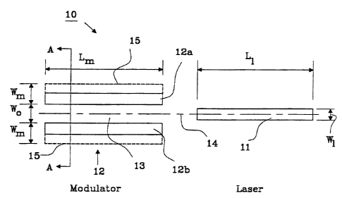
Fig. 2 shows a part of an insulating mask layout consisting of
a plurality of circuit masks 10 for manufacturing a laser and
a modulator according to the present invention. The circuit
mask 10 comprises two masking parts, a laser part 11, which
covers and protects a first set of layers, forming the laser,
during subsequent manufacturing steps, and a modulator part
12, which defines an area 13 where a second set of layers
forming the modulator is to be manufactured. The area 13 being
in a light transmission direction of the laser, illustrated
with a line 19.
CA 02352228 2001-05-28
WO 04/38284 PCT/SE99/02377
7
The dimensions, length L1 and width W1 of the laser masking
part 11, are substantially equal across, dependent on the type
of the implemented laser, to protect the laser when the
modulator is manufactured. The mask dimensions for a
distributed feedback laser having a band-gap energy
corresponding to a wavelength of approximately 1550 nm may, as
an non-limited example, be L~ ~400um and W1 ~l2um.
The modulator masking part 12 consists in this example of two
separate parts 12a and 12b, having essentially equal
dimensions and being arranged on equal distances to the line
14 with a fixed intermediate distance W". Each mask having a
selected length Lm, arranged in parallel with the line 14, and
a selectable width W", preferably in the interval 0-20 um. The
dashed line 15 indicating the upper limit of the width.
The selectable width is used for changing the composition and
the thickness of grown layers close to the masks, especially
in the area 13, during a selective area growth process. As is
described earlier, in the background to the invention, an
increase of substances with a shorter diffusion length will
occur close to the masks, as well as a general increase of
material. A preferred intermediate distance W~, between the
modulator masking parts 12a, 12b is in the range of 1 to 3
times of said shorter diffusion length, and may obtain a good
composition of an optical waveguide layer in the modulator and
good pace in epitaxial growth.
The semiconductor substrate is preferable made of indium
phosphide (InP), and the optical waveguide layer in the
modulator is preferable made of indium gallium arsenide
phosphide InxGal_.,AsyPi-y, where x, y have a value ranging from 0
3U to l, InGaAsP in short.
CA 02352228 2001-05-28
WO 00/38284 PCT/SE99102377
8
A certain increase in the width of the modulator masking part
corresponds to an increased wavelength close to said modulator
masking part 12, when growing a waveguide layer.
When a plurality of photonic devices, comprising a laser and a
modulator, are to be implemented on the same substrate, where
the first set of layers for the laser is manufactured in a
first step and the optical waveguide layer for the modulator
have been found out to have the variations shown in Fig. 1,
the composition of the waveguide layer in all areas intended
to be used as modulators may need to be compensated. This
compensation is performed by selecting the width of the
modulator masks to correspond to the wavelength compensation
needed dependent on the position on the substrate.
Fig. 3a and 3b are cross-sections along line A-A in Fig. 2
according different implementations of the present invention
using the mask in Fig. 2 as non-limited examples where:
an intermediate distance - W~, = 20 um, and
a modulator mask width - Wn, = 10 um.
In Fig. 3a, the inventive mask M is arranged directly on a
semiconductor substrate 30. This can be achieved by forming
the first photonic device, providing a protective insulating
film mask over said device, and etching the substrate clean
from any material not protected by said insulating masks.
In Fig. 3b, the inventive mask M is arranged on layers of
material L, remains of the laser fabrication, at the same time
as the protective insulating film is arranged on top of the
first set of layers forming the laser. The areas not covered
by the inventive mask M or the protective mask is etched down
to the substrate 30.
CA 02352228 2001-05-28
WO 00/3$284 PCT/SE99/02377
9
Thus, both of these implementations creates an equivalent
modulator during the selective area growth process described
below.
During selective area growth of a modulator, using the above
masking particulars, a number of layers are obtained
consisting, for instance, of n-InP/InGaAsP/p-InP on a
semiconductor substrate 30 of n-InP, where n-InP is an indium
phosphide layer doped with a surplus of electrons and p-InP is
an indium phosphide layer with a surplus of holes.
lU The first layer 31 of n-InP is called a spacer, which is used
to make the surface under the next layer 32, waveguide layer,
as free of defects as possible. If the substrate is of a very
high quality this layer may be omitted.
Increased thickness of the deposited material 34 can be seen
at the edges of the mask due to surface diffusion. This
variation in thickness is negligible since only a narrow
portion of the material between the masks is used for
manufacturing the modulator. Furthermore there is an increase
in the modulator height Hm compared to the overall height H~"
2U which is due to the shorter diffusion length of indium, which
in turn gives an enrichment of indium close to the masks.
Fig. 4a and 4b shows a comparison between a normal and a
compensated waveguide layer in a modulator according to the
present invention, where the overall increased wavelength
clearly can be seen as well as the compensating effect of the
variable width of the modulator masks.
Fig. 4a shows values of a measurement of wavelength ~, as a
function of y-axis of the modulator waveguide layer. The
values are presented along the y-axis crossing the centre of
CA 02352228 2001-05-28
WO 00/38284 PCT/SE99/02377
the substrate (x=0). The lower line 40 represents a normal
substrate without any compensating masks during the selective
area growth process. The values of the wavelength are
decreasing when going from right to left, as shown in Fig. 1
5 going from the top to the bottom. On the other hand, the upper
line 41, which represent a compensated waveguide layer, shows
only a variation of 10-11 nm over the same distance as the
lower line varies almost 40 nm.
Fig. 4b shows values of a measurement of wavelength ~, as a
10 function of x-axis of the modulator waveguide layer. The
values are presented along the x-axis crossing the centre of
the substrate (y=0). The lower line 42, representing the same
normal substrate as measured in Fig. 4a, have a maximum at
x=0, and decreases when going to the right and the left, as
shown in Fig. 1. On the other hand, the upper line 43, which
represents the compensated waveguide layer, only shows a
variation of 10-11 nm over the same distance as the lower line
varies almost 25 nm. ,
The result of these measurements shows that a compensated
waveguide layer may be manufactured to obtain a considerable
lower variations in wavelength variations across a wafer,
where the selective area growth process, without any
compensating masks, achieve a large variation in wavelength,
i.e. band-gap energy.
A fundamental part of the inventive method is to characterise
the variations in band-gap energy across the substrate on a
reference substrate, to be able to select the desired width of
the compensating masks. This characterisation can be done by
forming a plurality of a first photonic device on a reference
substrate, cover said first device and then form a second
photonic device, as described in the preamble of claim l, and
CA 02352228 2001-05-28
WO 00/38284 PCTlSE99/02377
7. 1
thereafter measure the wavelength in the selected area for the
second photonic device, by photo luminescence measuring
techniques.
The inventive method may naturally fully compensate the
S wavelength in the waveguide layer of the modulator, so as the
difference in wavelength, the so called detuning, between the
laser and the modulator is reduced to an acceptable level, for
instance approximately 60 nm.