Note: Descriptions are shown in the official language in which they were submitted.
07/19/01 15:31 FAX 418 882 7881 CA 02352241 2001-05-22 f~,
.. . - . ~002/O11
Pressure sensor
The invention refers to a non-capsulated housingless pressure sensor for
measuring the pressure in a liquid or gaseous medium and, in particular, to
a pressure sensor with a resistance unit of strip conductors arranged on a
substrate in the form of a semiconductor chip.
In measuring liquid pressure, e.g. blood pressure within a blood vessel, it
is known to use a pressure sensor within a catheter, which comprises a
semiconductor chip having a resistance unit provided thereon. Below the
resistance unit, the semiconductor chip forming the substrate is provided
with a recess so that a very thin wall thickness is given at the measuring
site.
Due to the action of the pressure, the thin wall is bent, whereby different
degrees of extension occur in the resisters of the resistance unit. Thus, it
is possible to determine the pressure acting on the substrate from the voltage
change measured at the resistance unit. The substrate is adhered tv a support
wall which may in turn be situated in a catheter, the resistance unit being
located on the side ofthe substrate averted from the support wall. Since this
side is exposed to the medium whose pressure is to be measured, ft is coated
with an additional passivation layerthat prevents contact between the medium
and the resistance unit or the substrate, respectively. It is true that all
electric
components of the pressure sensor are covered, but electrocorrvsion can
occur, in particular when the pressure sensor is operated in electrically
conductive liquids, which electrocorrvsion may cause a loss of the sensor or
an inherent sensor drift. Moreover, possible damages ofthe passivation layer
have a direct effect on the functional behavior of the sensor. Finally, the
use
ofsuch pressure sensors in the blood circulation poses certain problems, since
fluid-related erroneous measurements and deposition of blood components
may occur.
From DE 39 37 522 Al, a semiconductor pressure sensor is known that has
a support wall and a semiconductor substrate. A pressure transmission opening
is provided in the substrate. The opening is formed as a recess in the
substrate
07/19/01-'15:31 FAX_ 418 882 7861 ~ pp352241.2001-05-22 -__ _ _ ..~003/O11
2
and delimited by a membrane. The resistance unit is located on the side of
the substrate that abuts on the support wall. Between the substrate and the
support wall, an elastomer seal is provided. However, the latter does not
extend
over the membrane region.
It is the object ofthe present invention to provide a non-capsulated
housingless
pressure sensor that is insensitive to damage and which can, in particular,
be used as a small-sized high precision sensor.
According to the present invention, the object is solved with the features of
claim 1.
In the present pressure sensor, the side ofthe substrate on which the
resistance
unit is provided faces the support wall, with an elastic intermediate layer
being
provided between the support wall and the substrate. With this pressure
sensor,
the electric components provided on the substrate are protected between
the substrate and the support wall. Should external influences cause damages
to the sensor, these remain non-critical for the function because only the
top surface of the substrate or the chip is affected. Because of the protected
ZO accommodation ofthe resistance unit, the sensor can be operated in
electrically
conductive liquids, without electrocorrosion causing sensor loss or an
inherent
sensor drift. In as far as insulating layers are required, these can be kept
extremely thin. The present housingless pressure sensor design results in
a small-sized and flat arrangement and can be integrated in a thin support
wall of a few tenths of a millimeter without protruding. The support wall may
be planar or bent at a tube. Further, the pressure sensor is insensitive to
light,
since the electrically and possibly photogalvanically active surtace is
arranged
in a light-tight manner between the substrate and the support wall. The
present
invention provides for an extremely flat sensor means without any additional
sensor housing, the sensor means even being adapted to measure pressures
in electrically conductive media. The insulating intermediate layer between
07/19/01 15:52 FAX 418 882 7881 CA 02352241 2001-05-22 _ _ -_ X004/011
3
the support wall and the substrate is elastic. This means that this
intermediate
layer allows for certain movements of the sensor relative to the support wall
so that the substrate is held on the support wall in a floating manner, so to
speak. Thereby, the sensor is mechanically decoupled from the support wall
and it is made sure that mechanical or temperature-related deformations
of the support wall cause no substantial electrical signals. Preferably,
silicone
material is used for the intermediate layer.
According to a preferred embodiment of the invention, the resistance unit
is provided on a thin membrane of the substrate which is flush with the
substrate surface facing the support wall, a recess being provided behind
the membrane. The diameter of the recess is in the order of 0.1 to 0.6 mm
so that the recess is too small to reach and damage the sunk-in thin membrane
with usual tools such as pincers.
1~
Another advantage is that wires connected to the bottom surface of the
substrate can be glued or cemented directly to the support wall, whereby
stress relief is obtained at the connection site. Further, the connection area
whose insulation is critical, is mechanically protected due to its being
arranged
20. between the substrate and the support wall.
The present pressure sensor may be designed as an absolute pressure sensor.
Here, the recess in the substrate is evacuated and covered with a vacuum-tight
layer. On the other hand, it is possible to design the pressure sensor as a
25 differential pressure sensor, where both sides of the support wall, and
thus
also both sides of the thin membrane, are subjected to different pressures.
The following is a detailed description of embodiments of the invention with
reference to the drawings.
In the Figures:
07/19/01 15: a2 FAX 418 882 7881 ~ 02352241 2001-05-22 I~,
_. ~005/O11
4
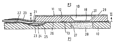
Fig. 1 is a sectional view through a first embodiment ofthe pressure sensor
designed as an absolute pressure sensor,
Fig. 2 is a bottom view on the substrate from the direction of the arrow
II-II in Fig. 1, and
Fig. 3 is a sectional view of a pressure sensor designed as a differential
pressure sensor.
The pressure sensor of Figs.1 and Z has a support wall 10 that forms a barrier
between a pressure PI on one side of the support wall and the environment.
It is assumed that the pressure P2 prevails in the environment. The support
wall 10, preferably only a few tenths of a millimeter in thickness, is made
of a rigid gas-tight material, in particular of metal. It may be planar, yet
it
is also possible to provide a cylindrical or otherwise shaped member.
A chip li is provided on the support wall 10, comprising a substrate 12 with
an electrical resistance unit 14 on the bottom surface 13 facing the support
wall 10, as illustrated in Fig. 2. The substrate 12 is made ofhighly pure
silicon
and has a thickness of about 200 Nm. In the present case, it is a rectangular
disc of 1,x+00 Nm x 600 ~m in size. The substrate lz is provided with strip
conductors 15 applied using the deposition and etch processes conventional
with semiconductor production. Together with the strip conductors 15, contact
surfaces 16 are formed that may be connected to external wires. The strip
conductors 15 are further connected to resistor bridges 17 tv farm a bridge
circuit. In the present case, four resistor bridges 17 are provided, forming
a conventional bridge circuit. The resistor bridges 17 comprise narrow, and
thus high-ohmage sections of the strip conductors 15. The resistance bridges
17 are provided in the region ofa membrane I8. This membrane 18 comprises
a thin wall of the substrate 12 left in the region of a recess 19. The recess
i9 corresponds to a truncated pyramid with inclined flanks 20. The length
07/19/01 15:32 FAX 418 _882 7681 ca, o2s5224i 2ooi-o5-22 _ 1~J008/O11
S
of the edges is 250 Nm. The thickness of the membrane 18 is about 10 Nm.
The membrane 18 extends on the bottom surface of the substrate 12 so that
this lower side is smooth overall, i.e. it presents no indentations or
protrusions.
S The conductors 21 of sensor wires 22 are planarly bonded or connected to
contact surtaces I6. These sensor wires 22 have their insulations fixed on
the support plate 10 by means of an epoxy adhesive 23. In the support plate
10, a cutout 24 is provided into which the conductors 21 enter so that their
ends are accommodated below the substrate 12. The cutout 24 is filled with
an insulating and elastic plastics mass 2S similar to that of the elastic
intermediate layer 26.
Between the bottom surface 13 of the chip l I and the support wall 10, another
elastic intermediate layer 26 of silicon material is provided. This layer Z6
extends
iS over the entire bottom face ofthe substrate 12, including the membrane 18.
The chip I1 is supported floating on the intermediate layer 26.
In the support plate 10, a pressure transmitting opening 27 is provided below
the membrane 18 that extends through the entire thickness of the support
plate. The pressure transmitting opening 27 is filled with a filling 28
consisting
ofthe material of the intermediate Payer 26 or ofa pressure transmitting gel.
The bottom side of the filling 28 is flush with the bottom side of the support
wall 10. As a result, the medium delimited by the support wall 10 cannot enter
the pressure transmitting opening 27 and cannot deposit there. Moreover,
high flew rates at the bottom side of the support plate cannot lead to
pressure
artefacts because of the step-less transition between the support plate and
the filling 28.
The top surface of the chip 11 that forms the rear side, is covered with a
vacuum-tight layer 29 that may also be made of silicon. This layer 29 closes
the recess 19 off to the outside. The recess 19 is evacuated. The pressure
07/19/01 15:52 FAX 418 882 7881 ~ 02352241 2001-05-22 _ ~007/O11
G
acting vn the membrane 18 via the filling 28 is the pressure P1 and the
deformation of the membrane 18 depends exclusively on this pressure P1.
Accordingly, the pressure sensor is an absolute pressure sensor.
Fig. 3 illustrates the embodiment of Fig. 1 in a modified form as a
differential
pressure sensor. Here, the layer 29 has been omitted so that the pressure
P1 acts on one side of the membrane and the pressure P2 acts on the rear
side of the membrane. The differential pressure sensor thus measures the
difference P1 minus P2. Here, the recess 1.9 may be filled with a pressure
transmitting gel 30 or with silicone.