Note: Descriptions are shown in the official language in which they were submitted.
CA 02352521 2001-07-06
TITLE OF THE INVENTION
Phosphor Thin Film, Preparation Method, and EL Panel
BACKGROUND OF THE INVENTION
Technical Field
This invention relates to a light-emitting layer for
use in inorganic EL devices, and more particularly, to a
phosphor thin film used as a light-emitting layer and an EL
panel using the same.
Background Art
In the recent years, active research works have been
made on thin-film EL devices as small-size and large-size,
lightweight flat displays. A monochromatic thin-film EL
display using a phosphor thin film of manganese-doped zinc
sulfide capable of emitting yellowish orange light has
already become commercially practical as a dual insulated
structure using thin-film insulating layers 2 and 4 as
shown in FIG. 2. In FIG. 2, a predetermined pattern of
lower electrodes 5 is formed on a substrate 1, and a first
insulating layer 2 is formed on the lower electrodes 5. On
the first insulating layer 2, a light-emitting layer 3 and
a second insulating layer 4 are successively formed. On
the second insulating layer 4, a predetermined pattern of
upper electrodes 6 is formed so as to construct a matrix
circuit with the lower electrodes 5.
Thin-film EL displays must display images in color in
order that they find use as computer, TV and similar
monitors. Thin-film EL displays using sulfide phosphor
thin films are fully reliable and resistant to environment,
but at present regarded unsuitable as color displays
because EL phosphors required to emit light in the
primaries of red, green and blue have poor characteristics.
Engineers continued research on SrS:Ce (using SrS as a
-1-
CA 02352521 2001-07-06
matrix material and Ce as a luminescent center) and ZnS:Tm
as a candidate for the blue light-emitting phosphor, ZnS:Sm
and CaS:Eu as a candidate for the red light-emitting
phosphor, and ZnS:Tb and CaS:Ce as a candidate for the
green light-emitting phosphor.
These phosphor thin films capable of emitting light
in the primaries of red, green and blue suffer from
problems of emission luminance, emission efficiency and
color purity. Thus color EL panels have not reached the
commercial stage. Referring to the blue color among
others, a relatively high luminance is achieved using
SrS:Ce. However, its luminance is still short as the blue
color for full-color displays and its chromaticity is
shifted toward green. There is a desire to have a better
blue light-emitting layer.
To solve the above problem, thiogallate and
thioaluminate base blue phosphors such as SrGaZS4:Ce,
CaGaZS4 : Ce , and BaAIZS4 : Eu were developed as described in
JP-A 7-122364, JP-A 8-134440, Shinshu Univ. Technical
Report, EID 98-113, pp. 19-24, and Jpn. J. Appl. Phys.,
Vol. 38 (1999), pp. L1291-1292. From the BaAlZS4:Eu
phosphor, light of CIE1931 chromaticity coordinates (0.12,
0.10) is obtained. However, there is a need for a blue
phosphor having a higher color purity. If blue light
having a higher purity, especially blue light having
CIE1931 chromaticity coordinates of x < about 0.2 and y
0.10, that is, NTSC blue of (0.14, 0.08) is developed, then
a display of better quality becomes available.
SUNll~IARY OF THE INVENTION
An object of the invention is to provide a phosphor
thin film eliminating a need for filters, having a
satisfactory color purity and useful as the blue color in
full-color EL displays, a method for preparing the same,
and an EL panel.
This and other objects are attained by the present
-2-
CA 02352521 2001-07-06
invention which is defined below as (1) to (6).
(1) A phosphor thin film formed of a matrix material
comprising barium thioaluminate as a main component and
having europium added thereto as a luminescent center, said
matrix material further containing magnesium.
(2) The phosphor thin film of (1) wherein magnesium
is added in such an amount as to give an atomic ratio
Mg/(Ba+Mg) between 0.05 and 0.8.
(3) The phosphor thin film of (1) or (2) which emits
blue light having chromaticity coordinates of x < 0.2 and y
< 0.10.
(4) An EL panel having the phosphor thin film of any
one of (1) to (3).
(5) A method for preparing the phosphor thin film of
any one of (1) to (3) by an evaporation process,
placing at least an aluminum sulfide source, a barium
sulfide source having a luminescent center added thereto,
and a magnesium metal source in a vacuum chamber, and
evaporating aluminum sulfide, barium sulfide and
magnesium metal from the respective sources and depositing
the evaporated substances on a substrate while binding the
substances together, thereby forming a sulfide phosphor
thin film.
(6) A method for preparing the phosphor thin film of
any one of (1) to (3) by an evaporation process,
placing at least a barium thioaluminate source having
a luminescent center added thereto and a magnesium metal
source in a vacuum chamber, and
evaporating barium thioaluminate and magnesium metal
from the respective sources and depositing the evaporated
substances on a substrate while binding the substances
together, thereby forming a sulfide phosphor thin film.
BRIEF DESCRIPTION OF THE DRAWINGS
FIG. 1 is a schematic cross-sectional view showing an
exemplary construction of the apparatus to which the method
-3-
CA 02352521 2001-07-06
of the invention is applicable or the manufacturing
apparatus of the invention.
FIG. 2 is a partially cross-sectional, perspective
view showing an exemplary construction of the inorganic EL
device which can be manufactured by the method and
apparatus of the invention.
DESCRIPTION OF THE PREFERRED EMBODIMENTS
Several embodiments of the invention are described in
detail.
The invention provides a means of adding magnesium to
a barium thioaluminate-base EL material for further
improving the luminance and blue color purity thereof.
The phosphor thin film of the invention is formed of
a barium thioaluminate-base matrix material having europium
added thereto as a luminescent center and further having
magnesium added thereto.
Examples of the barium thioaluminate used in the
phosphor thin film of the invention include Ba5AlzSe,
Ba4AlZS, , Ba2A1zS5 , BaA12S4 , BaAl4S, , Ba4Al14Sz5 , BaA18S13 , and
BaAl12S19. The matrix material may use these compounds alone
or in admixture of two or more and take an amorphous state
where a distinct crystalline structure is absent.
Also oxygen may substitute for sulfur in barium
thioaluminate to convert it to barium aluminate. Also
acceptable is an oxysulfide intermediate barium aluminate
and barium thioaluminate.
The phosphor thin film of the invention is arrived at
by adding magnesium to the above-described matrix material
and is preferably represented by the compositional formula:
( Ba , Mg ) xAlYOZSW : Eu .
In the formula, x, y, z and w denote molar ratios of
elements Ba, A1, O and S, and are preferably in the ranges
of
x = 1 to 5 ,
y = 1 to 15,
-4-
CA 02352521 2004-02-27
z = 0 to 30, and
w = 3 to 30.
Preferably magnesium is added in such an amount that
the atomic ratio of Mg to Ba in the barium thioaluminate
_ 5 matrix material, as expressed by Mg/(Ba+Mg), may fall in
the range between 0.05 and 0.8, especially between 0.3 and
0.6.
Magnesium is effective for shifting the EL emission
spectrum to the shorter wavelength side. When magnesium is
added to barium thioaluminate, the matrix material is
increased in band gap so that the europium added may
undertake effective transition within the compound crystal
field, producing Light emission of shorter wavelength.
The amount of europium added as a luminescent center
is preferably 0.5 to 10 atom% based on (Ba+Mg) atoms.
The phosphor thin film of the invention can emit
light of blue color having a high purity, that is, CIE1931
chromaticity coordinates of x < 0.2, especially x = 0.1 to
0.2, and y < 0.10, especially y = 0.02 to 0.1. That is,
emission of blue light approximate to the NTSC blue (0.14,
0.08) is possible. The emission of blue light having such
a high purity eliminates a need for filters, contributing
to the manufacture of applied devices of improved quality
and reduced cost.
The phosphor thin film is preferably prepared, for
example, by an evaporation process to be described below.
More particularly, a barium thioaluminate pellet
having europium added is prepared. The pellet is
evaporated in a vacuum chamber by irradiating electron
beams, and at the same time, magnesium metal is evaporated
by resistive heating for thereby adding magnesium. The
amount of Mg added is adjusted by previously measuring the
deposition rates of vapor substances from the EB source and
the resistive heating source, and controlling the powers to
the respective sources on the basis of the measured rates.
HZS gas may be admitted during the evaporation.
-5-
CA 02352521 2001-07-06
Alternatively, a multi-source reactive deposition
process is employable. Exemplary is a ternary evaporation
process using a barium sulfide pellet having europium added
thereto, aluminum sulfide and magnesium. More
specifically, a sulfide phosphor thin film is formed by
placing at least an aluminum sulfide source, a barium
sulfide source having a luminescent center added thereto,
and a magnesium metal source in a vacuum chamber, and
evaporating aluminum sulfide, barium sulfide and magnesium
metal from the respective sources and depositing the
evaporated substances on a substrate while binding the
substances together.
Europium added to the source substance may take the
form of metal, fluoride, oxide or sulfide. Since the
amount of europium added varies depending on the source
substance and the thin film to be deposited, the
composition of the source substance is adjusted so as to
achieve an appropriate dosage.
During the evaporation, the temperature of the
substrate may be at room temperature to 600°C, preferably
300 to 500°C. If the substrate temperature is too high,
the thin film of matrix material may have more asperities
on its surface and contain pin holes therein, giving rise
to the problem of current leakage on EL devices. Also the
thin film can be colored brown. For this reason, the
aforementioned temperature range is preferable. Also
preferably, the film deposition is followed by annealing.
The preferred annealing temperature is 600°C to 1,000°C,
and more preferably 600°C to 800°C.
The oxide phosphor thin film thus formed is
preferably a highly crystalline thin film. Crystallinity
can be evaluated by x-ray diffraction, for example. To
promote crystallinity, the substrate temperature is set as
high as possible. It is also effective to anneal the thin
film in vacuum, N2, Ar, air, sulfur vapor or HzS after its
-6-
CA 02352521 2001-07-06
formation.
It is also preferred to carry out anneal treatment on
the Mg-added barium thioaluminate thin film in an oxidizing
atmosphere such as oxygen or air after its formation and in
combination with the anneal treatment. For example, once a
thin film is formed by a binary reactive deposition process
using a barium sulfide pellet having Eu and Mg added
thereto, an aluminum sulfide pellet and hydrogen sulfide
(HzS) gas, it may be annealed in air.
Further, it is preferred to produce the phosphor thin
film of the invention by alternately forming magnesium
sulfide films and barium thioaluminate films, and annealing
the multilayer structure into a Mg-added barium
thioaluminate thin film.
Still further, it is preferred to produce the
phosphor thin film of the invention by alternately forming
magnesium thioaluminate films and barium thioaluminate
films, and annealing the multilayer structure.
When annealed at 400 to 800°C, magnesium diffuses
through the multilayer structure to promote crystallization
and achieve a blue shift of the emission spectrum.
The aforementioned annealing treatment is effective
for outstandingly increase the EL light emission luminance
of the phosphor thin film. The annealing treatment
promotes crystallization of the EL thin film and introduces
oxygen into the alkaline earth thioaluminate. In addition,
the rare earth added as the luminescent center possesses
effective transition within compound crystals, producing
light emission at a high luminance. For example, where Eu
is the luminescent center, Euz+ contributing to blue light
emission is stabilized in the EL thin film.
The light emitting device has a lifetime in that the
luminance drops with the lapse of light emitting time. The
composition in which sulfur and magnesium are co-present
with oxygen improves the lifetime performance and prevents
the luminance from dropping. As compared with the matrix
CA 02352521 2001-07-06
material of pure sulfide, the matrix material having
magnesium or an oxygen compound incorporated therein is
stable in air. This is probably because the stable oxide
component protects the sulfide component in the film from
oxygen. Therefore, according to the inventors'
investigation, an optimum value exists between the sulfide
and magnesium and optionally, oxide composition.
The contents of sulfur and oxygen in the matrix
material may be adjusted at the stage of the raw material
composition or by forming the thin film and then effecting
anneal treatment on the thin film under controlled
conditions.
No particular limits are imposed on the thickness of
the light emitting layer. However, too thick a layer
requires an increased drive voltage whereas too thin a
layer results in a low emission efficiency.
Illustratively, the light emitting layer is preferably
about 100 to 2,000 nm thick, especially about 150 to 700 nm
although the thickness varies depending on the identity of
the fluorescent material.
The pressure during evaporation is preferably
1 . 33x10-4 to 1 . 33x10-1 Pa ( 1x10⁻⁶ to 1x10⁻³ Torr) . When a gas
such as HZS is introduced, the pressure may be adjusted to
6. 65x10-3 to 6 . 65x10-2 Pa ( 5x10⁻⁵ to 5x10⁻⁴ Torr) . If the
pressure exceeds the range, the operation of the electron
gun becomes unstable, and composition control becomes very
difficult. The rate of gas feed is preferably 5 to 200
standard cubic centimeters per minute (SCCM), especially 10
to 30 SCCM although it varies depending on the power of the
vacuum system.
If desired, the substrate may be moved or rotated
during evaporation. By moving or rotating the substrate,
the deposited film becomes uniform in composition and
minimized in the variation of thickness distribution.
When the substrate is rotated, the number of
revolutions is preferably at least about 10 rpm, more
_g_
CA 02352521 2001-07-06
preferably about 10 to 50 rpm, and especially about 10 to
30 rpm. If the rotational speed of the substrate is too
high, there may arise a problem of seal upon admission into
the vacuum chamber. If the rotational speed of the
substrate is too low, compositional gradation may occur in
the thickness direction within the chamber so that the
characteristics of the light emitting layer may become
poor. The means for rotating the substrate may be any
well-known rotating mechanism including a power source such
as a motor or hydraulic rotational mechanism and a power
transmission/gear mechanism having a combination of gears,
belts, pulleys and the like.
The means for heating the evaporation source and the
substrate may be selected, for example, from tantalum wire
heaters, sheath heaters and carbon heaters, as long as they
have the predetermined thermal capacity, reactivity or the
like. The temperature reached by the heating means is
preferably in the range of about 100 to about 1,400°C, and
the precision of temperature control is about ~1°C,
preferably about ~0.5°C at 1,000°C.
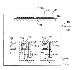
FIG. 1 illustrates one exemplary construction of the
apparatus for forming the light emitting layer according to
the invention. Reference is made to an embodiment wherein
Mg-added barium aluminate:Eu is produced by using aluminum
sulfide, barium sulfide and magnesium as the evaporation
sources and admitting HZS during evaporation. In the
illustrated embodiment, a substrate 12 on which the light
emitting layer is to be deposited, EB evaporation sources
14 and 15, and a resistive heating evaporation source 16
are disposed within a vacuum chamber 11.
In the resistive heating evaporation source 16 having
a heater (not shown) mounted therearound, a metal
(magnesium) 16a is contained to constitute the magnesium
evaporation source.
The electron beam (EB) evaporation sources 14 and 15
serving as means for evaporating aluminum sulfide and
_g_
CA 02352521 2001-07-06
barium sulfide include crucibles 40 and 50 which contain
barium sulfide 14a having a luminescent center added
thereto and aluminum sulfide 15a, and electron guns 41 and
51 having electron emitting filaments 41a and 51a built
therein, respectively. Built in the electron guns 41, 51
are mechanisms for controlling electron beams. To the
electron guns 41, 51 are connected ac power supplies 42, 52
and bias power supplies 43, 53. The electron guns 41, 51
produce electron beams alternately at predetermined powers
in a controlled manner, for evaporating the barium sulfide
14a having a luminescent center added thereto and the
aluminum sulfide 15a in a predetermined ratio. Although
the evaporation sources are controlled by two electron guns
in the illustrated embodiment, multi-source simultaneous
evaporation using a single electron gun is also possible.
The evaporation process of the latter is known as multi-
source pulse evaporation process.
In the illustrated embodiment, the evaporation
sources 14, 15, 16 are depicted, for the convenience of
illustration, at positions corresponding to discrete local
areas of the substrate. Actually, the evaporation sources
are located such that the deposited film may become uniform
in composition and thickness.
The vacuum chamber 11 has an exhaust port 11a through
which the chamber is evacuated to establish a predetermined
vacuum in the chamber. The vacuum chamber 11 also has an
inlet port 11b through which a reactant gas such as
hydrogen sulfide is admitted into the chamber.
The substrate 12 is fixedly secured to a holder 12a.
The holder 12a has a shaft 12b which is rotatably held by
an outside rotating shaft mount (not shown) so that the
vacuum may be maintained in the chamber 11. The shaft 12b
is adapted to be rotated at a predetermined number of
revolutions by a rotating means (not shown). A heating
means 13 in the form of a heater wire is closely secured to
the substrate holder 12a so that the substrate may be
-10-
CA 02352521 2001-07-06
heated and maintained at the desired temperature.
Using the illustrated apparatus, vapors of barium
sulfide, aluminum sulfide and magnesium are evaporated from
the EB evaporation sources 14, 15 and resistive heating
source 16 and deposited on the substrate 12 where they are
bound together to form a magnesium-added barium
thioaluminate fluorescent layer. By rotating the substrate
12 during the evaporation process if desired, the light
emitting layer being deposited can be made more uniform in
composition and thickness distribution.
There have been described the fluorescent thin film
material and the method of manufacture by evaporation
according to the invention, by which a phosphor thin film
having a higher luminance and a further improved color
purity of blue can be easily formed.
Using the phosphor thin film of the invention as a
light emitting layer 3, an inorganic EL device is
manufactured, for example, to the structure shown in FIG.
2. Between the substrate l, electrodes 5, 6, thick-film
insulating layer 2 and thin-film insulating layer 4, there
may be disposed intermediate layers such as a layer for
enhancing bond, a layer for mitigating stress, and a layer
for preventing reaction. The thick film may be improved in
smoothness as by polishing its surface or using a smoothing
layer.
FIG. 2 is a partially cross-sectional, perspective
view showing an exemplary construction of the inorganic EL
device using the light emitting layer of the invention. In
FIG. 2, a predetermined pattern of lower electrodes 5 is
formed on a substrate 1, and a first thick insulating layer
(or thick-film dielectric layer) 2 is formed on the lower
electrodes 5. On the first insulating layer 2, a light-
emitting layer 3 and a second insulating layer (or thin-
film dielectric layer) 4 are successively formed. On the
second insulating layer 4, a predetermined pattern of upper
electrodes 6 is formed so as to construct a matrix circuit
-11-
CA 02352521 2001-07-06
with the lower electrodes 5.
Any desired material may used as the substrate as
long as the substrate has a heat resistant temperature or
melting point of at least 600°C, preferably at least 700°C,
especially at least 800°C so that the substrate may
withstand the thick-film forming temperature, the forming
temperature of the EL fluorescent layer and the annealing
temperature of the EL device, the substrate allows
deposition thereon of functional thin films such as a light
emitting layer by which the EL device can be constructed,
and the substrate maintains the predetermined strength.
Illustrative examples include ceramic substrates of glass,
alumina (A1z03), forsterite (2MgO~SiOz), steatite
( Mg0 ~ Si02 ) , mullite ( 3A1z03 ~ 2Si02 ) , beryllia ( Be0 ) , aluminum
nitride (AlN), silicon nitride (SiN), and silicon carbide
(SiC+Be0) as well as heat resistant glass substrates of
crystallized glass or the like. Of these, alumina
substrates and crystallized glass substrates having a heat
resistant temperature of higher than about 1,000°C are
especially preferable. Where heat transfer is necessary,
berillia, aluminum nitride, silicon carbide and the like
are preferred.
Also useful are quartz, heat oxidized silicon wafers,
etc. as well as metal substrates such as titanium,
stainless steel, Inconel and iron base materials. Where
electro-conductive substrates such as metal substrates are
used, a structure in which a thick film having an internal
electrode is formed on a substrate is preferred.
Any well-known thick-film dielectric material may be
used as the thick-film dielectric material (first
insulating layer). Materials having a relatively high
permittivity are preferred.
For example, lead titanate, lead niobate and barium
titanate based materials can be used.
The dielectric thick film has a resistivity of at
-12-
CA 02352521 2001-07-06
least 108 S2 ~ cm, especially about 101° to 1018 S2 ~ cm. A
material having a relatively high permittivity as well is
preferred. The permittivity s is preferably about 100 to
10,000. The preferred thickness is 5 to 50 Vim, especially
10 to 30 Vim.
The insulating layer thick film is formed by any
desired method. Methods capable of relatively easily
forming films of 10 to 50 ~m thick are useful, and the sol-
gel method and printing/firing method are especially
preferred.
Where the printing/firing method is employed, a
material is fractionated to an appropriate particle size
and mixed with a binder to form a paste having an
appropriate viscosity. The paste is applied onto a
substrate by a screen printing technique, and dried. The
green sheet is fired at an appropriate temperature,
yielding a thick film.
Examples of the material of which the thin-film
insulating layer (second insulating layer) is made include
silicon oxide (SiOz), silicon nitride (SiN), tantalum oxide
( TaZ05 ) , strontium titanate ( SrTi03 ) , yttrium oxide ( Y203 ) ,
barium titanate (BaTi03), lead titanate (PbTi03), PZT,
zirconia (Zr02), silicon oxynitride (SiON), alumina (A1203),
lead niobate, PMN-PT base materials, and multilayer or
mixed thin films of any. In forming the insulating layer
from these materials, any of conventional methods such as
evaporation, sputtering, CVD, sol-gel and printing/firing
methods may be used. The insulating layer preferably has a
thickness of about 50 to 1,000 nm, especially about 100 to
500 nm.
The electrode (lower electrode) is formed at least on
the substrate side or within the first dielectric. As the
electrode layer which is exposed to high temperature during
formation of a thick film and during heat treatment along
with the light emitting layer, there may be employed a
-13-
CA 02352521 2001-07-06
customary metal electrode containing as a main component
one or more elements selected from palladium, rhodium,
iridium, rhenium, ruthenium, platinum, tantalum, nickel,
chromium and titanium.
Another electrode layer serving as the upper
electrode is preferably a transparent electrode which is
transmissive to light in the predetermined emission
wavelength region because the emitted light often exits
from the opposite side to the substrate. When the
substrate is transparent, a transparent electrode may also
be used as the lower electrode because this permits the
emitted light to exit from the substrate side. Use of
transparent electrodes of ZnO, ITO or the like is
especially preferred. ITO generally contain Inz03 and Sn0
in stoichiometry although the oxygen content may deviate
somewhat therefrom. An appropriate proportion of Sn02
mixed with Inz03 is about 1 to 20~, more preferably about 5
to 12~ by weight. For IZO, an appropriate proportion of
Zn0 mixed with Inz03 is generally about 12 to 32~ by
weight.
Also the electrode may be a silicon-based one. The
silicon electrode layer may be either polycrystalline
silicon (p-Si) or amorphous silicon (a-Si), or even single
crystal silicon if desired.
In addition to silicon as the main component, the
electrode is doped with an impurity for imparting electric
conductivity. Any dopant may be used as the impurity as
long as it can impart the desired conductivity. Use may be
made of dopants commonly used in the silicon semiconductor
art. Exemplary dopants are B, P, As, Sb, Al and the like.
Of these, B, P, As, Sb and A1 are especially preferred.
The preferred dopant concentration is about 0.001 to 5 ate.
In forming the electrode layer from these materials,
any of conventional methods such as evaporation,
sputtering, CVD, sol-gel and printing/firing methods may be
used. In forming a structure in which a thick film having
-14-
CA 02352521 2001-07-06
an internal electrode is formed on a substrate, the same
method as used in forming the dielectric thick film is
preferred.
The electrode layer should preferably have a
resistivity of up to 1 S2~cm, especially about 0.003 to 0.1
S2~cm in order to apply an effective electric field across
the light emitting layer. The preferred thickness of the
electrode layer is about 50 to 2,000 nm, especially about
100 to 1,000 nm.
Although the light emitting layer of the invention is
applied to inorganic EL devices in the illustrated
embodiment, it may be applied to another type of device as
long as the phosphor thin film of the invention can be used
therein, and especially to blue light emitting devices,
which can be applied to full-color display panels.
EXAMPLE
Examples are given below for illustrating the
invention in more detail.
Example 1
An exemplary evaporation chamber which can be used in
the manufacturing method of the invention is illustrated in
FIG. 1. There were used a two-point controlled gun and a
resistive heating source.
An EB source 15 containing BaS powder having 5 mold
of Eu added, another EB source 14 containing A12S3 powder,
and a resistive heating source 16 containing Mg were placed
in a vacuum chamber 11. The materials were simultaneously
evaporated from the respective sources, and deposited on a
rotating substrate heated at 150°C, forming a
(Ba,Mg)A12S3:Eu layer. The rates of evaporation from the
respective sources were adjusted so as to provide a
deposition rate of 1 nm/sec for (Ba,Mg)A12S3:Eu. During
evaporation, HZS gas was admitted at 10 SCCM. After the
thin film was formed, it was annealed at 750°C for 10
-15-
CA 02352521 2001-07-06
minutes in an Ar atmosphere.
The ( Ba, Mg ) A12S3 : Eu thin film formed on a Si
substrate as a monitor was analyzed for composition by x-
ray fluorescence to find an atomic ratio of Ba:Mg:Al:S:O:Eu
- 5.32:4.16:22.15:12.02:56.17:0.17. It was a barium
thioaluminate film containing a substantial amount of
oxygen.
Using this light emitting layer, an EL device of the
structure shown in FIG. 2 was fabricated.
For both the substrate and the thick-film insulating
layer, a BaTi03 base dielectric material having a
permittivity of 5,000 was commonly used. A Pd electrode
was used as the lower electrode. The device was fabricated
by furnishing a sheet for the substrate, and forming the
lower electrode and thick-film insulating layer on the
sheet by a screen printing technique to form a green sheet,
followed by co-firing. The surface was polished, yielding
a substrate bearing a thick-film first insulating layer of
30 ~m thick.
On this substrate, a phosphor thin film (light
emitting layer) was formed to 300 nm by the same procedure
as above.
Then a second insulating layer thin film was formed
on the phosphor thin film. Taz05 was used for the second
insulating layer thin film, and a Taz05 film of 200 nm
thick was formed. By RF magnetron sputtering technique
using an ITO oxide target, a transparent ITO electrode of
200 nm thick was formed on the second insulating layer thin
film at a substrate temperature of 250°C, completing the EL
device.
When an electric field having a frequency of 1 kHz
and a pulse width of 50 ~S was applied across the
electrodes, the EL device emitted blue light having a
luminance of 200 cd/m2 and CIE1931 chromaticity coordinates
(0.1347, 0.0789). The spectrum of light emission had a
peak wavelength of 464 nm.
-16-
CA 02352521 2001-07-06
An EL device, which was similarly fabricated without
addition of Mg, emitted blue light having CIE1931
chromaticity coordinates (0.1197, 0.1366), and the spectrum
of light emission had a peak wavelength of 474 nm. It is
evident that the addition of Mg leads to blue light of
higher purity.
Example 2
(Ba,Mg)A12S3:Eu was formed as in Example 1 except
that an EB gun was used instead of the two-point controlled
gun, and a resistive heating source containing an Eu-doped
barium thioaluminate pellet and Mg was used. Four light
emitting layers were formed in which the atomic ratio
Mg/(Mg+Ba) was changed from 0 to 0.1, 0.3 and 0.5. The
resulting EL devices were evaluated in terms of blue light
emission.
The spectrum of light emission of the EL devices in
which the atomic ratio Mg/(Mg+Ba) was 0, 0.1, 0.3 and 0.5
had a wavelength of 472 nm, 471 nm, 470 nm and 460 nm,
respectively. The addition of Mg shifts the spectrum to
the shorter wavelength side. The EL device having an
atomic ratio Mg/(Mg+Ba) of 0.5 produced blue light of a
high purity close to the NTSC blue.
The phosphor thin film of the invention offers a
phosphor thin film material capable of emitting blue light
having a high color purity without a need for filters and a
high luminance.
BENEFITS OF THE INVENTION
The invention provides a phosphor thin film
eliminating a need for filters, having a satisfactory color
purity and useful as the blue color in full-color EL
displays, a method for preparing the same and an EL panel.
-17-