Note: Descriptions are shown in the official language in which they were submitted.
CA 02353140 2001-07-16
1
OPTICAL CONNECTOR ADAPTER
BACKGROUND OF THE INVENTION
1. Field of the Invention
The present invention relates to optical connectors and,
more particularly, to an, adapter for connecting optical
connectors to another member.
2. Brief Description of Prior Developments
U.S. Patent 5,873,746 discloses a backpanel connector
with a spring biased housing moveable in a Z direction.
U.S. Patent 4, 432, 604 discloses a self-adjusting
fiberoptic connector assembly having optical fiber plugs
connected to a backplane by movable brackets. U.S.
Patent 5,828,805 discloses a multifiber optical connector
plug. U.S. Patent 4,361;372 disc:Loses a connector panel
for an electronic cabinet having apring-loaded cells for
a floating plate on a connector panel. Fig. 5 show a
conventional optical connector adapter available from FCI
USA, Inc. of Etters, Pennsylvania as part number 86144.
The adapter comprises two plastic pieces 2,3 connected to
each other by two retaining springs 4. The retaining
springs 4 have barbs 5. The member 2 also has board
contact surfaces 6. When the adapter is inserted into a
through-hole of a printed circuit :board or backplane, the
contact surfaces 6 and the barbs 'i are adapted to locate
portions of the backplane thE:rebetween to thereby
stationarily attach the adapter to the backplane.
Problems exist with conventional optical fiber connector
adapters in that alignment is sometimes unsatisfactory
and latching of optical connectors to the adapter is
CA 02353140 2001-07-16
2
sometimes unsatisfactory. Conventional multi-connection
adapters can comprise multi-piece frames which use epoxy
to assemble the frames. Frame assembly takes up
manufacturing time and can create quality control
prob 1 ems. Conventional adapters also do not necessarily
provide adequate connector float in an axis of connector
insertion (z-axis float) . TherE: is a desire for an
adapter frame to have a stronger body, better latching
and better alignment. There is a7!so a desire for spring
action of individual adapter housings to compensate for
various optical connector connection conditions and allow
for greater z-axis float of optical connectors being
attached to the adapter. In addition, there is a desire
to provide a faster assembly process for assembling an
optical fiber connector adapter with greater quality
control and without use of epoxy.
SUMMARY OF THE INVENTION
In accordance with one embodiment of the present
invention, an optical connector adapter is provided for
connecting optical connectors to each other. The adapter
comprises a main section having a through channel for
receiving mating ends of the optical connectors. The
main section comprises resilient optical connector
latches extending into the through channel. The adapter
also comprises at least one projeci=ion extending from the
main section. The at least one projection includes a
fastener mounting area and a spring support area. A
fastener can attach the at least one projection to an
electrical component. A spring c;an be -located between
the spring support area and the electrical component to
bias the adapter at a first position relative to the
electrical component.
CA 02353140 2001-07-16
3
In accordance with another embodiment of the present
invention, an electronic and optical component system is
provided comprising an electronic component; and an
optical connector adapter assembly connected to the
electronic component. The assembly comprises a housing
and at least one spring. The housing comprises resilient
optical connector latches and is suitably sized and
shaped to removably receive at least two mating optical
connectors. The housing is movably mounted in a hole
through the electronic component. The at least one
spring biases the housing relative to the electronic
component in a predetermined direction.
In accordance with one method of the present invention, A
method of assembling a backplane assembly comprising
steps of providing an optical connector adapter having a
housing with a through channel for receiving two mating
optical connectors in opposite directions; movably
mounting the housing directly in a hole of an electronic
component; and biasing the housing in a predetermined
direction relative to the electronic component, wherein
the housing can slidingly move along the electronic
component in the hole.
BRIEF DESCRIPTION OF T13E DRAWINGS
The foregoing aspects and other features of the present
invention are explained in the following description,
taken in connection with the accompanying drawings,
wherein:
Fig. 1 is an exploded partial perspective view of a
system incorporating features of the present invention;
CA 02353140 2001-07-16
4
Fig. 2 is a perspective partial view o ~ one of the
elect ronic component assemblies shown in Fig. 1
incorporating features of the present invent=ion;
Fig. 3 is a partially exploded perspectiv a view of the
optical connector adapter shown in Figs. 1 and 2;
Fig. 4 is a partial cross-sectional view of one of the
fastener mounting areas of the adapter shown in Fig. 3;
and
Fig. 5 is a perspective view of a conventional optical
connector adapter available from FC;I USA, Inc. of Etters,
Perms ylvania as part number 86144.
DETAILED DESCRIPTION OF THE PREFERRED EMBODIMENT
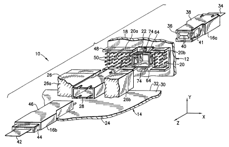
Referring to Fig. l, there is shown an exploded
perspective view of a system 10 incorporating features of
1S the present invention. Although the pre sent invention
will be described with reference to the single embodiment
shown in the drawings, it should be under stood that the
present invention can be embodied in many alternate forms
of embodiments. In addition, any suitable size, shape or
type of elements or materials could be used.
The system 10 generally comprises at least one first
electronic assembly 12, at least one second electronic
assembly 14, and at least one mat~eable pair of optical
connector assemblies 16a, 16b. The first assembly 12 is
preferably a backplane assembly or mother printed circuit
board assembly comprising a printed circuit board 18, at
least one electrical connector 20 and at least one
optical connector adapter 22. The second assembly 14 is
preferably a daughter printer circuit board assembly
CA 02353140 2001-07-16
compr~.-sing a printed circuit board 24, at least one
elect r ical connector 26, and an optical connector outer
housing 28. The optical connector outer housing 28 is
fixed and stationarily mounted i;.o a side 30 of the
5 daughter board 24 and extends pass= a leading edge 32 of
the daughter board 24. However, in a alternate
embodiment the outer housing 28 coul d be movably
connected to the daughter board 2~4. In this embodiment
the daughter board electrical connector 26 has two
sections 26a, 26b. Both section~~ 26a, 26b are fixedly
attached to the side 30 of the daughter board 24 and have
front ends which extend past the leading edge 32 of the
daughter board 24. In this embodiment the two sections
26a, 26b have the optical connector outer housing 28
therebetween. However, in alternate embodiments the
connector 26 might only have one section and/or the outer
housing 28 could be located other than between the
sections 26a, 26b, and/or the outer housing 28 could be
integrally formed with the housings) of the connector
section (s) . The connector 26 preferably comprises a
dielectric plastic housing and electrical contacts. The
contacts preferably comprise first ends connected to the
daughter board 24 and second female ends for removable
connection with the contacts of the: connector 20.
The first optical connector assembly 16a generally
comprises an optical cable assembly 34, an inner ferrule
optical conductor and housing subassembl y 36, and an
outer housing 38. Optical conductors 40 from the optical
cable assembly 34 extend to the front face of the
subassembly 36. The subassembly 36 is preferably spring
loaded in the outer housing 38 towards a forward position
in a known manner. The outer housing 38 includes lateral
side latch areas 41 for removably latching the outer
CA 02353140 2001-07-16
6
housing 38 with the adapter 22. However, in alternate
embodiments any suitable type of optical connector
assembly or its components could be used. The second
optical connector assembly 16b generally comprises an
optical cable assembly 42, a subassembly 44, and a
housing 46. Optical conductors of the cable assembly 42
extend to the front end of the subassembl y 44. As with
the assembly 16a, the optical conductors are sandwiched
between ferrules of the subassembly 44. The subassembly
is preferably spring loaded towards a forward position in
the housing 46. __The housing 46 is preferably snap-lock
removably mounted into the outer housing 28 to attach the
second optical connector 16b to t:he daughter board 24.
In an alternate embodiment any suitable type of second
optical connector 16b and/or outer housing 28 could be
used. The outer housing 28 preferably comprises lateral
side latch areas (not shown), similar to latch areas 41
on the outer housing 38, for removably latching the outer
housing 28 with the adapter 22. Examples of some types of
optical connectors and adapters are described in U.S.
Patent No. 5,828,805 and U.S. Patent Application Nos.
09/536,522; 09/608,666 and (Attorney Docket
No. 680-009355-US(PAR)) which are hereby incorporated by
reference in their entireties.
Referring now also to Figs. 2-4, in this embodiment the
electrical connector 20 generally comprises two sections
20a, 20b. However, in alternate embodiments the
connector 2 0 could include more or less than two
sections. Each section 20a, 20b generall y comprises a
housing 48 and contacts 50. In this- embodiment the
contacts 50 comprise male pins. However, any suitable
type of contacts could be used. The housings 48 form
receiving areas for receiving the leading ends of the
CA 02353140 2001-07-16
7
connector 26 to connect the male contacts 50 to the
female contacts in the connector 26. The mother board 18
comprises an aperture 52 between .its two opposite sides.
The housings 48 are located on opposite sides of the
aperture on a front side 54.
The adapter 22 generally comprise:> a housing 56, springs
58 and fasteners 60. The housing 56 is preferably a one-
piece molded plastic member comprising a main section 62
and projections 64. The main sE:ction 62 has a center
through-hole or through channel 66 with open opposite
ends 68, 69 and two pairs of resilient lateral side
latches 70, and 71; one pair proximate each end 68, 69.
The hole 66 is suitably sized and shaped to receive the
front ends of the optical connectors 16a, 16b therein
such that the optical connectors can be inserted into the
opposite open ends 68, 69 and can mate with each other
inside the hole 66. The latches 70, 71 can removably
retain the outer housing 28, 38 with the adapter housing
56 by resiliently positioning inside the latch areas 41
of the outer housings 28, 38. However, any suitable means
could be used to connect the outer housings 28, 38 or
optical connector assemblies 16a,, 16b to the adapter
housing 56. The projections 64 extend from opposite
sides of the main section 62.
As seen best in Fig. 4, each projection 64 generally
comprises a fastener mounting area 66 and a spring
support area 68. The fastener mounting area 66 includes
a through-hole with enclosed sides having a first section
70 and a second section 72. The two sections 70, 72 have
different cross-sectional areas. A fastener support ledge
71 is established between the two different cross-
sectional areas of the first and second sections 70, 72.
CA 02353140 2001-07-16
8
In this embodiment the first sect:ion 70 of the through-
hole is sized and shaped to a7.low the shaft of the
fastener 60 to pass therethrough. The second section 72
of the through-hole is sized and shaped to mateingly
receive a polygon sided nut 74 of the fastener 60
therein. The second section 72 and the nut 74 are
preferably suitably sized and shaped to press-fit the nut
74 into the second section 72 and prevent the nut 74 from
axially rotating. However, a.ny suitable type o.f
connection between the fastener 60 and the housing 56
could be provided. The spring su~,pport area 68 forms a
support surface for one end of 'the spring 58. In an
alternate embodiment, the springs) could be integrally
formed with the housing 56.
In this embodiment the springs 58 are comprised of coil
springs. However, any suitable type of springs could be
used. The springs 58 are located :between the projections
64 and the front side 54 of the mother board 18. The
fasteners 60 each generally comprise a bolt 76 and the
nut 74. The bolts 76 each have a shaft 78 which extends
through the mother board 18, through the center hole of
one of the springs, through the first section 70 of the
projections, and are threadingly connected to the nuts 74
in the second sections 72. The bolts 76 can
longitudinally slide through their respective holes in
the mother board 18. In alternate embodiments, any
suitable type of fasteners could be used to movably
connect the adapter housing 56 to the mother board 18.
In the embodiment shown the lateral sides 80 of the
projections 64 form bearing surfaces which can contact
the housings 48 of the connector sections 20a, 20b and
slide thereagainst. The main section 62 of the housing
CA 02353140 2001-07-16
9
56 extends through the aperture 52 in the motherboard 18.
More specifically, the main section 62 is longitudinally
slideable in the aperture 52 between a forward position
and a rearward position. The springs 58 bias the housing
56 in the forward position. However, the adapter housing
56 can longitudinally move relative to the connector 20
and mother board 18 towards a reward position, (Z-axis
movement) when the second assembly 14 is being connected
to the first assembly 12, with the springs 58 being
compressed and the bolts 76 sliding relative to the
mother board 18._ Rear surfaces 82 on the projections 64
can function as stops to limit reward movement of the
adapter housing 56. If the second assembly 14 is removed,
the springs 58 can bias the adapter housing 56 back to
its forward position.
The present invention allows for i~he adapter housing 56
to independently move in the Z-axi:> direction relative to
the connector 20 and mother board 18. This independent
Z-axis float can compensate for t=olerances between the
two assemblies 12, 14. The adapter housing 56 also
preferably maintains a fit inside the backplane aperture
52 to allow for the adapter housing 56 to move in the X
axis and Y-axis directions. Similar to the Z-axis float,
this can compensate for tolerances between the two
assemblies 12, 14.
With the present invention, the single piece adapter
housing design can provide a 'stronger body, better latch
and better optical connector alignment, then conventional
designs while still complying with backplane system
applications. The present invention can also allow for a
larger Z-axis float or movement than was available with
conventional designs. The present invention is not
CA 02353140 2001-07-16
necessarily limited to a backpl.ane adapter for only
optical connectors, but could be used as an adapter for
any suitable type of connectors. The springs 58 provide
a self-adjusting force and self-adjusting float for the
5 adapter. The adapter of the present invention could be
spaced from the electrical connecaor 20. However, the
combined electrical connector 20a, 20b and adapter 22
configuration provides a compact arrangement with the
electrical connector housings 48 aiding to locating the
10 movable adapter housing 56 relative to the electrical
connector housing,48 for easier initial insertion of the
connectors 26a, 26b, 16b/28 as a group or groups into the
housings 48, 56.
It should be understood that the foregoing description is
only illustrative of the invention.. Various alternatives
and modifications can be devised by those skilled in the
art without departing from the invention. Accordingly,
the present invention is intended to embrace all such
alternatives, modifications and variances which fall
within the scope of the appended claims.