Note: Descriptions are shown in the official language in which they were submitted.
CA 02353496 2007-07-12
1
SCALABLE DATA PROCESSING APPARATUS
The present invention concerns a scalable data processing apparatus,
particularly a data storage apparatus, comprising two or more thin-film
devices
which form a planar layer comprising a number of coextensive stacked
sublayers of thin film material, wherein the sublayers of each thin film
device
comprise electrical isolating and/or conducting and/or semiconducting
structures
and structures with information storage capability realized in the thin-film
material in a sublayer, wherein the structures register with or contact
electrically
other structures of this kind in adjacent sublayers in the stack forming the
thin
film device for realizing active and passive electronic circuit elements or
logic
cells in the thin-film device, wherein the active and passive circuit elements
in
the thin-film device have a three-dimensional architecture and extend through
two or more sublayers thereof, wherein the circuit elements are electrically
connected by horizontal electrical conducting structures in one or more
sublayers and vertical electrical conducting structures extending through one
or
more of the sublayers.
It is known in the art to create memory devices in the form of thin-film
circuits in
stacked configurations and wherein a memory device may additionally be
combined with processors for controlling, driving and addressing the memory,
but with the latter being realized in inorganic semiconducting materials, in
the
form of single crystal rigid substrates and/or thin-film provided on a carrier
substrate which very well may be exceptionally thin, for instance formed as
films
of silicon dioxide. A complete memory device with processing circuits is
created
by juxtaposition of the layers and often by transfer of the thin-film circuits
by
means of special methods. In order to provide interconnections between the
layers, vias through a set of holes in the layers are used and possibly
combined
with evaporation of metal in order to create the necessary current paths.
Furthermore, according to PCT/N099/00180, which belongs to the present
applicant, there is known an integrated scalable data processing device which
CA 02353496 2007-07-12
2
forms a complete computer with a mass memory and a combined processor and
memory module wherein in separate processor layers or separate memory
layers or combined processor and memory layers there are provided so-called
intelligent random access memories (IRAM) and processors which realize the
CPU function of the computer or which realize control and communication
functions in the computer. In order to provide short current paths, three-
dimensional electrical structures are used to create interconnections between
components in the separate layers and between the layers mutually. The whole
data processing device is provided on a substrate which contains further high-
speed processing circuits for control and communication purposes, these being
made of inorganic semiconducting materials according to conventional
technology, while the different layers of the data processing device are
otherwise wholly realized in thin-film technology regardless of whether they
concern processors or memories.
Further relevant prior art may be mentioned. US Patent No. 5,714,768
(Ovshinsky et al.) discloses a computational device with a processor and a
particular memory array in thin film technology mounted over the processor on
the top of the device and discloses the use of a memory medium based on
various inorganic materials which may attain different electrical resistance
values in response to selected electrical input signals to the separate memory
cells. Particularly, Ovshinsky et al. discloses special memory elements in the
form of so-called ovionic memories which are based on electrical phase change
and are made with inorganic chalcogenide compounds as switches. Each
memory element is conceived as a single unit and is encapsulated and mutually
isolated with insulating material, for instance of SiO2 or Si3N4. The memory
elements are arranged in a planar array structure which on each side is
contacted by an overlying grid of electrode structures, the electrode
structures in
each grid being oriented perpendicular to the electrode structure in the other
grid. Two dimensional memory arrays of this kind can now, with proper mutual
insulation, be stacked to form a vertical integrated memory structure provided
on
CA 02353496 2007-07-12
3
a substrate which may be a logic processing device comprising electronic
circuitry. No hint or suggestion is given in Ovshinsky et al. for stacking
thin film
devices made of coextensive thin film sublayers of thin film material or
wherein
the thin film devices comprise both circuit areas with active circuits and
memory
areas with memory modules realized by providing the sublayers of thin film
material with functional features according to purpose. Ferroelectric memory
devices, wherein a two dimensional memory cell array in a passive electrode
matrix is stacked to form a volumetric memory device, are moreover well known
in the art, for instance in US patent No. 5,329,485 (Isono et al.) and US
patent
No. 5,375,085 (Gnade et al.). Also, the use of ferroelectric polymer materials
for
erasable memories, particularly embodiments based on the use of
poly(vinylidene chloride) or poly(vinylidene trifluoroethylene) copolymers,
have
been proposed, e.g. in IBM Technical Disclosure Bulletin 37:421 424, No. 11
(1994). These polymers can be obtained as very thin films and the memory
medium provided as a continuous layer of thin film material with sets of
parallel
conducting electrodes deposited on either side and oriented mutually
orthogonally. Such two dimensional passive ferroelectric arrays can be stacked
to form a three dimensional structure. None of these above mentioned
publications, however, discloses thin film devices comprising sublayers with
functional features that will allow the realization of both active circuits
and
passive memory modules integrated in the thin film devices.
Finally, three dimensional memory processor structures based on transferred
thin film circuits are disclosed in international published application
W095/09438
(Zavracky et al.) and US patent No. 5,656,548 with the same inventors, both
publications being based on US patent application No. 130 033 of 30 September
1993, now abandoned. Particularly these publications disclose memory and
processor circuit layers stacked or interfoliated to form a three dimensional
structure, wherein the separate functional elements of the circuits are
fabricated
by patterning thin film materials using conventional planar circuit
technologies
CA 02353496 2007-07-12
4
and interconnecting vertically by e.g. metallic vias extending through the
structures.
Even though prior art devices for data processing and storage based on the use
of thin-film technology carry a number of advantages with regard to speed and
functionality, they are purely for storage purposes, often very costly and can
particularly be complicated to produce. An effective memory management
further requires a substantial processing capacity; for instance, for control,
communication and addressing, there are dedicated circuits for these purposes
often being assigned to a large memory or several separate memories with large
storage capacity.
The main object of the present invention is to provide a scalable data
processing
apparatus, particularly a data storage apparatus which is relatively simple
and
inexpensive to make and which in principle allows for almost unlimited scaling
of
the data storage capacity without the management and operation of the memory
becoming complicated.
A further object of the invention is to realize a scalable data processing
apparatus, particularly a data storage apparatus substantially in thin-film
technology which allows implementation of supporting functions for control and
addressing of memories realized in thin-film technology, the electronic
circuits
for the mentioned purposes to be integrated with memories in the thin-film
device.
Finally it is also an object of the present invention to realize a volumetric
data
storage device with large storage density, fast data access and high data
transfer rate, optionally combined with parallel input of data in the data
memory
and fast parallel readout of data therefrom.
According to the present invention, there is provided a scalable data
processing
apparatus, comprising at least two thin-film devices (1) which form a planar
layer
CA 02353496 2007-07-12
generated by a number of coextensive sublayers (S) that are stacked, each of
the sublayers (S) being made of a thin-film material, wherein the sublayers
(S) of
each thin-film device (1) comprises electrical isolating and/or conducting
and/or
semiconducting structures and structures with information storage capability
realized in the thin-film material, wherein the structures register with or
contact
electrically other structures of this kind in adjacent sublayers in the stack
forming
the thin-film devices (1) for realizing active and passive electronic circuit
elements or logic cells in the thin-film device, wherein the active and
passive
circuit elements in said at least two thin-film devices (1) are realized with
a
three-dimensional architecture and extend through two or more of said
sublayers (S), wherein the circuit elements are electrically connected by
horizontal electrical conducting structures in one or more sublayers (S) and
vertical electrical conducting structures extending through one or more of the
sublayers (S), said thin-film devices being stacked, said scalable data
processing apparatus being characterized in that each thin-film device (1)
comprises one or more memory areas (3), which form one or more matrix
addressable memories (3'), each with a memory medium (6) in a sublayer (S) in
contact with a first electrode set in the form of stripe-like parallel
electrical
conducting structures (7) or electrode structures and a second electrode set
(8)
in the form of corresponding electrode structures oriented substantially
orthogonal to the electrode structures (7) in the first electrode set, the
electrode
sets respectively being provided in further sublayers (S) adjacent to each
side of
the sublayer having the memory medium, whereby addressable memory cells
are created in the memory medium (6) at the crossings between the electrode
structures (7,8) in the first and the second electrode set, that each thin-
film
device (1) further comprises circuit areas (2) which form electronic thin-film
circuitry for controlling, driving and addressing the memory cells in one or
more
memories (3'), said electronic circuitry being connected with electrode
structures
(7,8) in respectively the first and the second electrode set in a memory (3')
via
current paths which are formed as electrical conducting structures in
substantially the same sublayers wherein the electrode sets are provided, and
CA 02353496 2007-07-12
6
that each thin-film device (1) has a respective interface to every other thin-
film
device in the apparatus, said interfaces being realized with communication and
signal lines and supporting circuitry for processing said lines and circuitry
being
provided in respective dedicated interface areas (4) in the thin-film device
(1).
Preferably, the apparatus is a data storage apparatus. In an advantageous
embodiment of the apparatus according to the invention, the memory medium in
one or more memories comprises materials selected among molecular materials
in the form of monomers, oligomers or polymers, carbon containing materials in
inorganic or organic form, or a juxtaposition or mixture of such materials. In
this
regard, it is preferred that the memory medium comprises a memory material
which, in a memory cell, provides a non-linear current/voltage characteristic,
said non-linear current/voltage characteristic being generated by inorganic or
organic diodes or a threshold-switchable material.
In another advantageous embodiment of the apparatus according to the
invention, the memory medium comprises a switchable material, said switchable
material being a non-volatile material, selected as a ferroelectric material
or a
charge transfer organic complex, or the memory medium can be switchable and
have a non-linear current/voltage characteristic.
In another advantageous embodiment of the apparatus according to the
invention, the electronic circuitry comprises inorganic and/or organic
semiconducting materials.
In an advantageous embodiment of the apparatus according to the invention,
the interface areas in one or more thin-film devices are integrated in an edge
portion of the one or more thin-film devices, said edge portions in the latter
case
registering mutually. In this regard, it is preferred that the interface area
in an
edge portion additionally comprises an I/O interface for the respective thin-
film
device or optionally the apparatus as a whole, and implements functions for
data
and signal communication with external and/or peripheral devices.
CA 02353496 2007-07-12
7
In another advantageous embodiment of the apparatus according to the
invention, the thin-film device or the stacked configuration of such devices
is
provided on a substrate which comprises active electronic circuits for
implementing additional control, driving and communication functions in the
apparatus, each thin-film device being connected with a circuit over a
separate
interface area which in each case extends vertically through the thin-film
devices
which are located between a given thin-film device and the substrate. In this
regard, it is preferred that the substrate comprises an interface portion
which
extends substantially horizontally in the substrate and parallel and adjacent
to
the thin-film device provided thereabove, and which is electrically connected
with the interface portions in the thin-film device or the thin-film devices
provided
above the substrate, and it is particularly preferred that the interface
portion
further comprises an I/O interface for the apparatus as a whole, said I/O
interface implementing functions for data and signal communication with
external and/or peripheral devices.
It is then also advantageous that the substrate is made of a semiconducting
material, particularly an inorganic single crystal semiconducting material and
even more particularly a silicon single crystal semiconducting material, and
it is
particularly preferred in this regard that the electronic circuits in the
substrate are
realized in CMOS technology. It is further preferred in this regard that
electrical
connections between the electronic circuits in the substrate and its interface
portion or over this interface portion to the interface areas in the above-
lying
thin-film devices are realized as CMOS-compatible metallic interconnections.
In an advantageous embodiment of the apparatus according to the invention,
the apparatus comprises two or more thin-film devices, the thin-film devices
being coextensive and provided mutually registering in the stack thereof. In
this
regard, it is preferred that one or more separation layers are provided
interfoliated between adjacent thin-film devices and that they implement
either
separately or in selected combinations an electrical, thermal, optical or
CA 02353496 2007-07-12
8
mechanical isolating function or a planarizing function, said interface areas
in
the respective thin-film devices in each case being electrically connected
through vias in a respective separation layer.
In another advantageous embodiment of the apparatus according to the
invention, the apparatus comprises two or more thin-film devices, the thin-
film
devices being provided mutually staggered in the stack thereof.
Preferably, the electrical connections between the thin film devices and/or
between an optional substrate are then provided extending horizontally and
vertically over the steps in the staggered stack.
It is then also preferred that one or more separation layers are provided
interfoliated between adjacent thin-film devices and separately or in selected
combinations implementing an electrical, thermal, optical or mechanical
isolating
or planarizing function, and that separation layers are only provided in the
overlapping portion of two adjacent thin-film devices, the interface areas of
the
respective thin-film devices being provided above exposed surface portions of
the thin-film devices in a staggered area thereof, such that the separation
layers
between the thin-film devices form an unbroken layer without vias for
electrical
connections between the separate thin-film devices.
Finally, in an embodiment of the apparatus according to the invention, the
apparatus is advantageously provided on a carrier substrate formed of a foil-
like
material or a rigid material such as silicon, said carrier substrate in each
case
being provided adjacent to the lowermost thin-film device in the stacked
configuration or an optionally provided substrate with electronic circuits.
The scalable data processing apparatus, particularly data storage apparatus
according to the invention, shall now be discussed in more detail in the
following
section with reference to exemplary embodiments and the accompanying
drawings
CA 02353496 2007-07-12
9
Fig. 1 a shows a plan view of a thin-film device used in the apparatus
according
to the present invention;
Fig. lb a section through a first embodiment of the thin-film device in Fig.
la,
taken along the line A-A;
Fig. 1 c a section through a second embodiment of the thin-film device in Fig.
1 a,
taken along the line A-A;
Fig. 2a a plan view of a third embodiment of the thin-film device used in the
apparatus according to the present invention;
Fig. 2b a section through the thin-film device in Fig. 2a, taken along the
line B-B;
Fig. 3a a fourth embodiment of the thin-film device used in the apparatus
according to the present invention;
Fig. 3b a section through the thin-film device in Fig. 3a, taken along the
line C-C;
Fig. 3c another section through the thin-film device in Fig. 3a, taken along
the
line D-D;
Fig. 4 schematically and in perspective an embodiment of a matrix addressable
memory as used in the thin-film device in one of the Figs. 1-3;
Fig. 5a a plan view of the matrix addressable memory in Fig. 4 connected with
an active electronic circuit in a thin-film device as shown in one Figs. 1-3;
Fig. 5b a schematic section through the memory in Fig. 5a, taken along the
line
E-E;
Fig. 6a a first embodiment of the apparatus according to the present
invention;
CA 02353496 2007-07-12
Fig. 6b a second embodiment of the apparatus according to the present
invention.
Fig. 6c shows a third embodiment of the apparatus according to the present
invention;
Fig. 7 a fourth embodiment of the apparatus according to the present
invention;
Figs. 8a and 8b variants of a fifth embodiment of the apparatus according to
the
present invention;
Fig. 9 schematically the joining of sublayers in thin-film technology into a
thin-
film device as used in the present invention and the joining of several such
thin-
10 film devices into an apparatus according to the invention;
Fig. 10 schematically a preferred embodiment of the apparatus according to the
present invention exploded into its main components.
The main object of the present invention is to provide a data storage device
and
the apparatus according to the invention will hereinbelow be considered to be
a
memory device and will be referred to as "apparatus". The basis of the present
invention is that the apparatus can be realized in the form of mutually
adjacent
and substantially parallel stacked layers, each of these stacked layers being
formed as a thin-film device which in turn is composed of a plurality of
sublayers
of thin film with specific and different functions and which are possibly made
of
different materials.
A thin-film device 1 as used in the present invention is shown in plan view in
Fig.
1 a. The thin-film device 1 is organized in a circuit area 2, memory areas 3
and
an interface area 4. In Fig. lb there is shown a section through the thin-film
device in taken along the line A-A of Fig. 1 a. The memory areas 3 which
contain
memories 3' realized in thin-film technology, are here shown provided within
the
circuit area 2 which contains thin-film based electronic circuitry for
implementing
CA 02353496 2007-07-12
11
control, communication and addressing functions for the memories. Depending
on the memory type, the addressing function will for instance comprise
writing,
reading and erasing in the memory, as well as communication to and from the
memory over the interface area 4. Fig. 1c shows a section through the thin-
film
device in Fig. 1 a, also taken along the line A-A, but here in another
embodiment
than that in Fig. lb. Here, the memory areas 3 here being shown with
vertically
stacked thin-film memories 3' in the circuit area 2, but mutually isolated by
electrical isolating layers 5. In this regard, it should also be understood-
that each
separate memory 3' is of course constituted by a number of separate sublayers,
as will be discussed in more detail in the following, and furthermore that the
electronic circuitry that is not particularly shown in the circuit area 2 not
only is
used for controlling and addressing of memories in the separate thin-film
device
via the interface area 4, but also communicates with corresponding circuitry
and
other memories in adjacently provided thin-film devices 1.
It may be that each separate thin-film device 1 is composed of a large number
of
sublayers, typically for instance several tens, while the separate memory 3'
does
not need to comprise more than four to five sublayers, which allows several
memories to be stacked, either vertically as shown in Fig. 1 c or in another
advantageous embodiment as shown in plan view in Figs. 2a and in cross-
sectional view along line B-B, in Fig. 2b. Here, the separate memories 3' in
the
thin-film device 1 are stacked, but mutually staggered. In Figs. 2a and 2b
there
are shown four memory stacks with four memories 3' mutually isolated by
electrical isolating layers 5. Only the lowermost memory and the uppermost
memory in each stack are indicated with the reference number 3'.
Another embodiment of the thin-film device 1 as used in the present invention
is
shown in Fig. 3a, which substantially corresponds to the embodiment of Fig.
2a,
with the memory stacks being created with the memories being staggered, but
now along a diagonal line such that the stack appears as shown in plan view in
Fig. 3a, in cross-sectional view along line C-C in Fig. 3b, and in cross-
sectional
CA 02353496 2007-07-12
12
view along line D-D in Fig. 3c. An arrangement of the memory in the stack as
shown in Fig. 2a and Fig. 3a can be advantageous with regard to better
exploitation of the real estate in the circuit area 2, while the staggering
can
simplify the interconnection between memories and electronic circuitry in the
circuit area 2. It is of course to be understood that the mutual arrangement
of the
memories 3' in the memory area 3 in the circuit area 2 is not essentially
limited
to some specific geometry, but may be varied within boundaries according to
the
embodiment and the form factor of the thin-film device 1.
Fig. 4 schematically shows the embodiment of an essentially passive matrix
addressable memory 3'. A memory of this kind is for instance disclosed in
PCT/N098/00185, which belongs to the present applicant. In Fig. 4, a memory
medium 6 is sandwiched between an underlying electrode set consisting of
parallel stripe electrodes 7 and an overlying electrode set consisting of
parallel
stripe electrodes 8. By applying voltages to an underlying and an overlying
electrode 7,8, a change of state will be obtained in the memory medium 6 at
the
crossing between the electrodes. The change of state for instance can be
expressed by a change of the impedance in the memory medium. The memory
medium 6 itself will preferably be made of a molecular material, or a
carbonaceous inorganic or organic material. Usually, it will be desirable that
the
memory medium shall have a non-linear impedance characteristic, and by
addressing a memory cell (not shown) formed in the crossing between an
underlying electrode 7 and an overlying electrode 8, it will be desirable to
prevent the generation of so-called sneak currents to other memory cells in
the
memory matrix. This can advantageously be achieved by providing the memory
medium with rectifying properties, preferably by incorporating a layer which
forms a diode junction or by the memory medium 6 itself spontaneously forming
a diode junction with the electrode material.
If the memory material 6 is a polymer, its information storage capability can
depend on a change of an impedance value of the material under applied
CA 02353496 2007-07-12
13
electric current or voltage, the material keeping this changed impedance value
after the current or voltage has been turned off. The memory can also be a
switchable material, for instance a ferroelectrical material in the form of a
polymer, the polarization state of which may represent a specific logic state,
or a
charge transfer metal organic complex such as M(TCNQ). Generally, there is
known in the art a number of different memory materials which may be used in
matrix addressable memories, and reference may be made in this regard to the
above mentioned publication PCT/N098/00185. In- Fig. 4 the memory is
provided in a sandwich arrangement, but this is, however, not a requirement
and
it is wholly possible to employ another electrode configuration, for instance
a
bridge configuration as disclosed in PCT/N098/00212, which belongs to the
present applicant and in which the underlying electrode 7 and the overlying
electrode 8 are mutually isolated in a crossing and the memory material 6 is
provided over the electrodes, which, of course, requires that the memory
material have the properties which ensure its information storage capability
also
in such a case. Typically, a memory material in this case may be a conjugated
polymer.
The interconnection between the memory 3' and a circuit 9 in the circuit area
2
is shown schematically and in plan view in Fig. 5a. Each of the electrodes 7,
8 in
the matrix is connected to the circuit 9 via word and bit line 10. Fig. 5b
shows a
cross-section taken along the line E-E of Fig. 5a. In Fig. 5b, the arrangement
is
formed as sublayers S1-S8 in the thin-film device 1. There are shown two
stacked memories 3' 1, 3'2 and the circuit 9, which are wholly realized in a
thin-
film technology. Particularly, it is to be observed that current paths and
conductor paths for the memory 3' that is underlying and overlying electrodes
7;8 as well as the lines 10 that connect the electrodes to the circuit 9, are
all
provided substantially in the same sublayer, here for instance S2, S4, S6 and
S8. This will make it easier to generate such current paths and conductor
paths
in the form of electrical conducting structures in one and the same sublayer,
according to purpose.
CA 02353496 2007-07-12
14
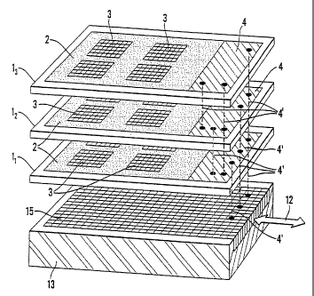
Fig. 6a shows how several thin-film devices 1, in this case three, are joined
into
a stacked configuration. As before, the circuit areas are denoted with 2 and
the
memory areas are denoted with 3 and in the figure are shown with mutual
registration, but this is not a requirement. The interface area 4 is provided
on the
side of the circuit areas and registers correspondingly, the electrical
connections
between the thin-film devices 1 being indicated schematically with arrows 4'
and
extending vertically through the interface area 4. Furthermore, the interface
area
4 can be made with I/O interfaces 12 which connect the thin-film devices 1
with
external devices (not shown) or peripheral devices (not shown) for input and
output of data.
Fig. 6b again shows the thin-film devices 1 in stacked configuration, but now
provided on a substrate 13 with active electronic circuits 14. This substrate
can
be realized well in an inorganic semiconducting material, for instance silicon
or
modifications of silicon, and the active electronic circuits can be realized
for
instance in CMOS technology. The active electronic circuits 14 in the
substrate
13 are intended for control and communication tasks in the management of
memories in the thin-film devices and are adapted for co-operating with thin-
film
circuits in the circuit areas 2 of the thin-film devices 1. This will leave
more room
in the thin-film devices 1 for memory purposes, as the thin-film circuits in
the
circuit areas 2 in this case can be restricted to that which is necessary in
order
to maintain an effective control and driving of the memory, while processing
tasks - for instance, with regard to parallel input and output of data to the
memory and for error correction, memory remapping etc. - may be handled by
processing devices implemented by the active electronic circuits 14 in the
substrate. Vertical interconnections 4' in the interface area 4 in the stacked
thin-
film devices communicate with an interface portion 15 on the substrate 13, and
the electrical connection through this interface portion and between the
circuits
14 and the vertical interconnections 4' can for instance be provided by
metallic
vias formed in the interface portion 15, but this must take place in a CMOS
compatible process if CMOS circuits are provided in the substrate. Instead of
CA 02353496 2007-07-12
creating the I/O-intertace 12 in the interface area 4 in the stacked thin-film
devices, this I/O-interFace 12 may now be provided in connection with the
interface 15 of the substrate.
Another embodiment of the apparatus according to the invention is shown in
Fig.
6c. Here, as before, are thin-film devices are provided in a stacked
configuration
on the substrate 13, but instead of providing, the interface area 4 of the
thin-film
devices 1 in an edge portion thereof, separate interface areas 4 are provided
in
order to create vertical interconnections between the thin-film devices 1 and
between these and the interface 15 in the substrate 13. This can in turn
10 contribute to a topologically regarded advantageous layout of the circuit
area in
the separate thin-film device and reduce the need for horizontal current paths
therein.
In a variant of the embodiment of Fig. 6c, the apparatus can be realized as
shown in Fig. 7. Here, separation layers 16 are provided between each thin-
film
device 1, such layers being known for instance from NO patent application no.
98 0781, which belongs to the present applicant. These separation layers can
either separately or in selected combinations implement for instance an
electrical, thermal, optical or mechanical isolating function. In a stacked
configuration, they may also be used as planarization layers. When the
interface
areas 4 in the thin-film devices 1 are provided as shown in Fig. 7, this
however
presupposes that they are passed through the separation layers 16 and this
must be done by interconnections, for instance in the form of vias in the
separation layers, which may be detrimental with regard to the isolating
function
and may additionally lead to cost-increasing fabrication steps. One way to
avoid
this is to provide thin-film devices 1 as before in the stacked configuration,
but
now mutually staggered.
An embodiment of this is shown in Fig. 8a, where the thin-film devices once
again are provided on a substrate 13 and are mutually separated by separation
layers 16, but where the interface area 4 is provided between the interface 15
in
CA 02353496 2007-07-12
16
the substrate 13 and above the exposed steps in the thin-film devices on the
side thereof. The interconnections between the thin-film devices 1 and between
the thin-film devices and the substrate 15 are schematically indicated by
horizontal and vertical interconnections 4'.
In the embodiment of Fig. 8a, there may also be a carrier substrate (not
shown)
adjacent to thin-film device 1 on the opposite side of the stacked
configuration.
For fabrication, the arrangement of the thin-film devices 1 can then take
place
from the carrier substrate (not shown) and upwards, whereafter the substrate
13
with active electronic circuits 14 is provided on top of the stacked
configuration
as a last step in the fabrication process. This implies that the
interconnections
over the interface area 4 and to the interface portion 15 are realized after
the
placement of the thin-film devices 1 in a preceeding fabrication step, which
in a
number of cases may be advantageous both with regard to costs and to
simplifying the creation of the interconnections.
Fig. 8b shows an embodiment approximately corresponding to that in Fig. 8a,
with thin-film devices 1 provided mutually separated by separation layers 16
and
once again provided staggered in a stacked configuration, such that the thin-
film
device 1 closest to the substrate 13 does not cover it wholly, but forms a
step
down to the surface of the substrate. Once again, the interface area 4 may be
provided above the stepped portions in the stacked configuration and
interconnections 4' may be provided between the thin-film devices 1 mutually
or
between the thin-film devices and the interface 15 in the substrate 13
extending
horizontally and vertically over the steps in the stacked configuration.
Fig. 9 shows quite schematically how each separate thin-film device 11, 12, 13
is constituted by a number of sublayers, here shown as four layers S1-S4.
Horizontal electrical conducting interconnections can be created as an
integral
part of a sublayer S by a conversion of thin-film material in this sublayer
and
corresponding vertical electrical conducting interconnections can be created
through the sublayers S by registering portions of electrical conducting
material
CA 02353496 2007-07-12
17
in the thin film. Under particular conditions, such electrical conducting or
semiconducting structures can be generated in situ in an already formed thin-
film stack or they can be generated separately in each separate sublayer S
which is then laminated or joined in another manner into a stack which forms a
thin-film device 1. In PCT/N099/00023, which belongs to the present applicant,
there is discussed a method for generating horizontal and vertical electrical
conducting structures in situ by means of radiation, for instance light
radiation or
particle radiation, for thus creating three-dimensional electrical conducting
and
semiconducting structures in a stacked thin-film device. The generation of
such
structures can however also take place by means of electric fields which are
applied spatially modulated in order to pattern the separate sublayer S by
means of a special generator/modulator device, such as is discussed in
PCT/N099/00022 which belongs to the present applicant.
The apparatus according to the present invention is shown in exploded view to
show its main components in Fig. 10, where it appears with three thin-film
devices 11, 12, 13 and the interface area 4 is provided in an edge portion of
the
thin-film devices. The apparatus in Fig. 10 is shown with the use of a
substrate
13 which comprises not shown active electronic circuits (not shown) and an
interface 15 and also forms the I/O interface 12 for the whole apparatus. The
use of a substrate 13 of this kind in the apparatus according to the present
invention is however not required, and the stacked configuration of the thin-
film
devices 1 may just as well be provided on a passive carrier substrate only,
for
instance one that is formed of a foil-like material or a rigid material such
as
silicon.
The embodiment of Fig. 10 has features similar to corresponding embodiments
as shown in the above-mentioned international patent application
PCT/N098/00185. In this patent application, there are disclosed in more detail
matrix addressable memory means which will be suited for use in the apparatus
according to the invention and there is also disclosed how circuits can be
CA 02353496 2007-07-12
18
realized in stacked thin-film layers and with three-dimensional topology. This
can
for instance concern diodes, transistors, complementary transistor circuits
and
logic gates realized in thin-film technology, which, however, shall not be
discussed in more detail here. It is also to be understood that memories in
the
separate thin-film device can be configured as one or more of a number of
memory types, viz. RAM, ROM, WORM, ERASABLE or REWRITEABLE or
combinations of such memories. Also, this is disclosed in detail in the above-
mentioned patent application and shall hence not be further described here. .
Each thin-film device 1 in the apparatus according to the invention can be
built
on its own separation layer 16 before the joining into a stacked configuration
takes place. The separate sublayers in a thin-film device 1 can have a
thickness
well below 1 pm, for instance down to 0.1 pm, which implies that a thin-film
device 1 provided on a carrier substrate or a substrate which could well
correspond to the separation layer 16, together with this substrate will
constitute
a component with a thickness of for instance 20 pm and may in that case
comprise more than 100 sublayers, which will be sufficient to realize
relatively
complicated electronic circuits in thin-film technology and simultaneously
allow
that tens of separate memories 3' can be stacked in each memory area 3. With
a memory cell size of 1 pm2 a single memory of 1 cm2, can then comprise for
instance 108 memory cells of this kind and consequently store at least 108
bits.
A thin-film device the size of a credit card will for instance comprise 40
such
separate memories and hence store 0.5 Gbytes. When the apparatus, which
can be implemented for instance as a PCMCIA-like card with 3 mm thickness,
can comprise 100 stacked thin-film devices, it will be seen that the apparatus
can store 50 Gbytes within the conditions given by the form factor. Increased
storage capacity can be obtained with better exploitation of the real estate
of
each thin-film device, that is by increasing the dimensions of the memory
areas
3, but also by a reduction in the size of the separate memory cell, to a size
of
about 0.25 pm x 0.25 pm or less, which seems realistic. In that case the
storage
capacity could be increased in a straightforward manner to 800 Gbytes, and it
CA 02353496 2007-07-12
19
and it will be seen that the apparatus according to the present invention thus
realized might enable a mass storage device or a hard disk replacement which
could be used in most of today's personal computers or workstations.
Under the conditions which follow from a given data storage density, it would
be
seen that the total data storage density will be given by the form factor, the
area
and the thickness of the apparatus. Basically and practically scaling to a
design
storage capacity will take place by using a sufficient number of thin-film
devices.
Integrated in a PCMCIA card type 3 for instance, the apparatus according to
the
invention could then replace a conventional hard disk memory in the card.
Where a given standard does not place restrictions on the dimensions, the
apparatus according to the invention could replace existing hard disk
solutions in
personal computers for instance and suitably scaled could offer mass storage
capacity in the Tbyte range.
Finally, it must be remarked that even though the apparatus according to the
invention is realized in a planar stacked configuration, it may also be
conceivable to form the stacked configuration in alternative geometries. As
the
thin films are made of a flexible material, if a substrate with active
circuits and
based on inorganic semiconductor=s is not used but for instance only a
flexible
carrier substrate in a form of foil like material is used, it is conceivable
that the
whole apparatus for instance may be rolled up into a cylinder or pipe like
configuration if this was advantageous for the purpose. In any case, it is
evident
that an apparatus according to the invention realized in flexible materials
can be
incorporated into other, and hence the apparatus can be used for implementing
applications in completely different circumstances than those which are
regarded to fall within the scope of conventional computer technology.