Note: Descriptions are shown in the official language in which they were submitted.
CA 02353535 2001-05-30
WO 00/34781 PCT/US99/27671
PATTERNED BINDING OF FUNCTIONALIZED
MICROSPHERES FOR OPTICAL DIFFRACTION-BASED
BIOSENSORS
TECHNICAL FIELD
The present invention is generally in the field of detecting
analytes in a medium and, more particularly, the present
invention relates to the use of functionalized microspheres for
enhancing optical diffraction with single use, disposable sensors
to indicate the presence of the analyte in a medium.
BACKGROUND OF THE INVENTION
There are many systems and devices available for
detecting a wide variety of analytes in various media. Most of
these systems and devices are relatively expensive and require a
trained technician to perform the test. There are many cases
where it would be advantageous to be able to rapidly and
inexpensively determine if an analyte were present. What is
needed is a biosensor system that is easy and inexpensive to
manufacture and is capable of reliable and sensitive detection of
analytes, including smaller analytes.
Sandstrom et al., 24 Applied Optics 472, 1985, describe
use of an optical substrate of silicon with a layer of silicon
monoxide and a layer of silicon formed as dielectric films. They
indicate that a change in film thickness changes the properties of
the optical substrate to produce different colors related to the
thickness of the film. The thickness of the film is related to the
color observed and a film provided on top of an optical substrate
may produce a visible color change. The authors indicate that a
mathematical model can be used to quantitate the color change,
and that "[c]alculations performed using the computer model
show that very little can be gained in optical performance from
using a multilayer structure... but a biolayer on the surface
1
CA 02353535 2001-05-30
WO 00/34781 PCTIUS99/27671
changes the reflection of such structures very little since the
optical properties are determined mainly by the interfaces inside
the multilayer structure. The most sensitive system for detection
of biolayers is a single layer coating, while in most other
applications performance can be by additional dielectric layers."
Sandstrom et al., go on to indicate that slides formed
from metal oxides on metal have certain drawbacks, and that
the presence of metal ions can also be harmful in many
biochemical applications: They indicate that the ideal top
dielectric film is a 2-3 nm thickness of silicon dioxide which is
formed spontaneously when silicon monoxide layer is deposited
in ambient atmosphere, and that a 70-95 nm layer silicon dioxide
on a 40-60 nm layer of silicon monoxide can be used on a glass
or plastic substrate. They also describe formation of a wedge
of silicon monoxide by selective etching of the silicon
monoxide, treatment of the silicon dioxide surface with
dichlorodimethylsilane, and application of a biolayer of
antigen and antibody. From this wedge construction they
were able to determine film thickness with an ellipsometer,
and note that the "maximum contrast was found in the region
about 65 nm where the interference color changed from purple
to blue." They indicate that the sensitivity of such a system is
high enough for the detection of protein antigen by immobilized
antibodies. They conclude "the designs given are sensitive
enough for a wide range of applications. The materials, i.e.,
glass, silicon, and silicon oxides, are chemically inert and do not
affect the biochemical reaction studied. Using the computations
above it is possible to design slides that are optimized for
different applications. The slides can be manufactured and
their quality ensured by industrial methods, and two designs are
now commercially available.
U.S. Patent 5,512,131 issued to Kumar et al. describes a
device that includes a polymer substrate having a metal coating.
An analyte-specific receptor layer is stamped on the coated
substrate. The device is used in a process for stamping or as a
switch. A diffraction pattern is generated when an analyte binds
2
CA 02353535 2008-01-16
to the device. A visualization device, such as a spectrometer, is
then used to determine the presence of the diffraction pattern..
However, the device described by Kumar et al. has several
disadvantages. One disadvantage is that. an extra visualization
device is needed to view any,diffraction pattern. By requiring a
visualization device, the Kumar et al. device does not allow a
large number of samples to be tested since it is not possible to
determine the presence of an analyte by using the unaided eye.
Additionally, this device is not able to detect smaller analytes as
these analytes do not produce a noticeable diffraction pattern.
U.S. Patent No. 5,482,830 to Bogart, et al., describes a
device that includes a substrate which has an optically active
surface exhibiting a first color in response to light impinging
thereon. This first color is defined as a spectral distribution of
the emanating light. The substrate also exhibits a second color
which is different from the first color (by having a combination
of wavelengths of light which differ from that combination
present in the* first color, or having a different spectral
distribution, or by having an intensity of one or more of those
wavelengths different from those present in the first color). The
second color is exhibited in response to the same light when the
analyte is present on the surface. The change from one color to
another can be measured either by use of an instrument, or by
eye. Such sensitive detection is an advance over the devices
described by Sandstrom and Nygren, supra, and allow use of the
devices in commercially viable and competitive manner.
However, the method and device described in the Bogart,
et al. patent has several disadvantages. One disadvantage is the
high cost of the device. Another problem with the device is the
difficulty in controlling the various layers that are placed on 'the
wafer so that one obtains a reliable reading. a _
Additionally, biosensors having a self-assembling
monolayer have been used to detect analytes and are set forth in
U.S. Patent No. 5,922,550.
However, these biosensors currently do not have the requisite
sensitivity required to detect smaller analytes since these smaller
3
CA 02353535 2001-05-30
WO 00/34781 PCTIUS99/27671
analytes do not produce a sufficient diffraction pattern to be
visible.
Some commercial lateral flow technologies have been
used which employ latex bead technology. These technologies
are currently employed in most of the commercially-available
home diagnostic kits (e.g. pregnancy and ovulation kits). These
kits use colored beads which accumulate in a defined "capture
zone" until the amount of beads becomes visible to the unaided
eye. However, these systems lack the requisite sensitivity to test
for many analytes, since a much larger number of latex beads
must bind in the capture zone to be visible to the naked eye than
that required to cause diffraction in the same size zone.
Generally, the number of beads needed is about 2 to 3 orders of
magnitude higher than the sensors of the present invention.
What is needed is a biosensor system that is easy and
inexpensive to manufacture and is capable of reliable and
sensitive detection of analytes, including smaller analytes.
SUMMARY OF THE INVENTION
- The present invention provides an inexpensive and
sensitive system and method for detecting analytes present in a
medium. The system comprises a biosensing device having a
polymer film upon which is printed a specific, predetermined
pattern of analyte-specific receptors. The polymer film may be
coated with a metal layer. Additionally, the system utilizes
"diffraction enhancing elements" which are capable of binding
to the target analyte and to the biosensor and are capable of
producing a substantial change in the height and/or refractive
index, thereby increasing the diffraction efficiency of the
biosensor and permitting the detection of smaller analytes. In
use, a target analyte attaches either to the diffraction enhancing
element, which then attaches to the biosensor, or directly to
select areas of the polymer film upon which the receptor is
printed. Then diffraction of transmitted and/or reflected light
occurs via the physical dimensions and defined, precise
placement of the analyte. A diffraction image is produced which
4
CA 02353535 2008-01-16
can be easily seen with the eye or, optionally, with a sensing
device.
The system of the present invention is much more
sensitive than current inexpensive systems. The system of the
present invention is able to detect low to high molecular weight
analytes, microorganisms, and DNA or RNA species in fluid
samples. More specifically, the system is able to detect
hormones, steroids, antibodies, drug metabolites, and even
nucleic acids, among others. This is a significant expansion of
the optical diffraction-based sensing technology set forth in U.S.
Patent No. 5,922,550.
The present invention utilizes diffraction enhancing
elements, such as latex microspheres, which aid in the detection
of smaller analytes. Normally, after an analyte binds to an
analyte-specific receptor on a biosensor, the analyte will diffract
or reflect transmitted light to produce a diffraction pattern. If the
analyte is larger, the diffraction pattern is able to be seen with the
unaided eye. However, some analytes are too small such that
the diffraction pattern produced is not able to be seen. By using
diffraction enhancing elements, the biosensor having the analyte-
specific receptor material may be used to detect these smaller
analytes. The diffraction enhancing elements used are capable of
binding to the analyte, and then the element with bound analyte
binds to the biosensor. Then, as the light is transmitted through
or reflected from the biosensor, the element enhances the
diffraction pattern generated by the analyte such that the
resulting diffraction pattern may be seen by the unaided eye.
The present invention also utilizes methods of contact
printing of patterned, analyte-specific receptors. The analyte-
specific receptors have receptive materials bound thereto. The
receptive materials are specific for a particular analyte or class of
analyte, depending upon the receptor used. Methods of contact
printing which would be useful in generating the sensing devices
used in the present system are disclosed fully in U.S. Patent
Nos. 6,020,047 and 6,048,623. However, since these methods
relate to self-assembling monolayers, the
5
CA 02353535 2001-05-30
WO 00/34781 PCT/US99/27671
methods need to be altered slightly, as discussed below, to print
the analyte-specific receptor material as this material is not self-
assembling.
Patterned analyte-specific receptor layers allow for the
controlled placement of analytes and/or diffraction enhancing
elements thereon via the patterns of analyte-specific receptors.
The biosensing devices of the present invention produced
thereby are used by first exposing the biosensing device to a
medium that contains the analyte of choice mixed with the
diffraction enhancing element. Then, after an appropriate
incubation period, a light, such as a laser or other point light
source, is transmitted through or reflected from the film. If the
analyte is present in the medium and is bound, either directly or
in conjunction with the diffraction enhancing element, to the
receptors on the patterned analyte-specific receptor layer, the
light is diffracted in such a way as to produce a visible image.
In other words, the analyte-specific receptor layers with the
analyte and/or diffraction enhancing element bound thereto can
produce optical diffraction patterns which differ depending on
the reaction of the receptors on the analyte-specific receptor
layer with the analyte of interest. The light can be in the visible
spectrum, and be either reflected from the film, or transmitted
through it, and the analyte can be any compound or particle
reacting with the analyte-specific receptor layer. The light can be
a white light or monochromatic electromagnetic radiation in the
visible region. While visible light is the desired light source, the
present invention may also be used with non-visible point light
sources, such as near-infrared light, coupled with a detector. The
thickness of the film and the size of the microparticle may be
adjusted to compensate for the non-visible light source.
Additionally, the present invention also provides a flexible
support for an analyte-specific receptor layer either directly on
the substrate or on gold or other suitable metal or metal alloy.
The present invention provides an analyte-specific receptor
layer on gold or other material which is suitable for mass
production. The biosensors used in the present invention can be
produced as a single test for detecting an analyte or it can be
6
CA 02353535 2001-05-30
WO 00/34781 PCT/US99/27671
formatted as a multiple test device. The biosensors of the
present invention can be used to detect (1) antigens or antibodies
associated with medical conditions, (2) contamination in
garments, such as diapers, and (3) contamination by
microorganisms.
In another embodiment of the present invention, nutrients
for a specific class of microorganisms can be incorporated into
the analyte-specific receptor layer. In this way, very low
concentrations of microorganisms can be detected by first
contacting the biosensor of the present invention with the
nutrients incorporated therein and then incubating, if necessary,
the biosensor under conditions appropriate for the growth of the
bound microorganism. The microorganism is allowed to grow
until there are enough organisms to form a diffraction pattern.
The present invention can also be used on contact lenses,
eyeglasses, window panes, pharmaceutical vials, solvent
containers, water bottles, adhesive bandages, and the like to
detect contamination.
These and other features and advantages of the present
invention will become apparent after a review of the following
detailed description of the disclosed embodiments.
BRIEF DESCRIPTION OF THE FIGURES
Figure I shows a biosensor capable of simultaneously
measuring several different analytes in a medium.
Figure 2 is a schematic of contact printing of analyte-
specific receptor layers.
Figure 3 is an atomic force microscopy image of
evaporated gold on MYLAR , purchased from Courtaulds
Performance Films (Canoga Park, CA). The average roughness
of the gold layer is 3-4 nanometers, with maximum roughness of
9 nanometers.
Figure 4 is an SEM photomicrograph showing patterned
attachment of diffraction enhancing elements in the presence of
an analyte.
7
CA 02353535 2001-05-30
WO 00/34781 PCT/US99/27671
DETAILED DESCRIPTION
The present invention features improved biosensing
devices, and methods for using such biosensing devices, for
detecting and quantifying the presence or amount of an analyte
of interest within a medium. The present invention is much
more sensitive and can be used to detect smaller analytes which,
until now, were not able to be detected without the use of
expensive instruments. The analytes that can be detected by the
present invention include, but are not limited to, hormones,
proteins such as antibodies, steroids, drug metabolites, nucleic
acids, microorganisms such as bacteria, yeasts, fungi and viruses.
In contrast to prior devices, those of the present invention allow
detection of extremely small quantities and sizes of analytes in a
medium in a rapid assay lasting only a few minutes. In addition,
no signaling or associated electronic components are required in
the present invention.
The present invention comprises micro-contact printing of
analyte-specific receptors onto polymer film, which may have a
metal coating thereon. The invention allows for the development
of single use, disposable biosensors based on light diffraction to
indicate the presence of the analyte. Additionally, the present
invention includes diffraction enhancing elements which increase
the diffraction efficiency of the biosensor, thereby making it
possible to detect any number of different analytes. Upon
attachment of a target analyte to select areas of the polymer film
which contain the receptor, either directly or in combination with
a diffraction enhancing element, diffraction of transmitted and/or
reflected light occurs via the physical dimensions and defined,
precise placement of the analyte. For example, yeast, fungi or
bacterium are large enough to act as diffraction elements for
visible light when placed in organized patterns on a surface.
However, smaller analytes, such as viruses, proteins, molecules,
hormones, steroids, drug metabolites and nucleic acids, are only
capable of acting as suitable diffraction elements when they are
also bound to a diffraction enhancing element. In addition to
producing a simple diffraction image, patterns of analytes can be
such as to allow for the development of a holographic sensing
8
CA 02353535 2001-05-30
WO 00/34781 PCT/US99/27671
image and/or a change in visible color. Thus, the appearance of
a hologram or a change in an existing hologram will indicate a
positive response. The pattern made by the diffraction of the
transmitted light can be any shape including, but not limited to,
the transformation of a pattern from one pattern to another upon
binding of the analyte to the receptive material. In particularly
preferred embodiments, the diffraction pattern is discernible in
less than one hour after contact of the analyte with the
biosensing device of the present invention.
The diffraction grating which produces the diffraction of
light upon interaction with the analyte and/or element should
have a minimum periodicity of the wavelength of incident light.
Very small analytes can be detected indirectly by using
diffraction enhancing element particles that are specific for the
small analyte. One embodiment in which the small analyte can
be detected comprises coating the element particle, such as a
latex bead, with a receptor material that specifically binds to the
analyte of interest.
A variety of methods may be used to attach the receptor
material onto the diffraction enhancing particle. These methods
include, but are not limited to, simple physisorption to a
hydrophobic particle (e.g., binding a protein onto polystyrene
particles); binding using a protein A or protein G linker; binding
using a streptavidin or avidin-biotin linker; or binding using
covalent attachment. A preferred embodiment of the present
invention is to use carbodiimide coupling of a proteinaceous
receptor to carboxylated particles. Other methods of coupling
well-known to those of ordinary skill in the art may be used as
well.
Diffraction enhancing element particles that can be used in
the present invention include, but are not limited to, glass,
cellulose, synthetic polymers or plastics, latex, polystyrene,
polycarbonate, bacterial or fungal cells and the like. The particles
are preferably spherical in shape, but the structural and spatial
configuration of the particle is not critical to the present
invention. For instance, the particles could be slivers, ellipsoids,
cubes, and the like. A desirable particle size ranges from a
9
CA 02353535 2001-05-30
WO 00/34781 PCT/US99/27671
diameter of approximately 0.1 m to 100.0 p.m, desirably
between approximately 0.3 m to 1 m. The composition of the
element particle is not critical to the present invention.
Preferably, the difference in refractive index between the
medium and the enhancing element is between 0.1 and 1Ø
More preferably, the difference in refractive index between the
medium and the enhancing element is between 0.2 and 0.7
The analyte-specific receptor layer on the polymer film
contains a receptive material, such as an antibody, that will
specifically bind to an epitope on the analyte that is different
from the epitope used in the binding to the particle. Thus, for
detecting a small analyte, such as viral particles, the medium is
first exposed to the diffraction enhancing element particles, such
as latex particles, to which the viral particles bind. Then, the
diffraction enhancing element particles are optionally washed and
exposed to the polymer film with the analyte-specific receptor
layers containing the virus specific antibodies. The antibodies
then bind to the viral particles on the element particle thereby
immobilizing the element particles in the same pattern as the
receptors on the film. Because the bound element particles will
cause diffraction of the visible light, a diffraction pattern is
formed, indicating the presence of the viral particle in the liquid.
Additionally, the polymer film may include a metal coating
thereon. The analyte-specific receptor layer would then be
located on the metalized surface of the film.
Alternatively, the analyte may be detected by first
exposing the substrate to the medium containing the analyte and
causing the analyte to bind to the analyte-specific receptor layer
material. Next, a solution containing the diffraction enhancing
element particles is contacted with the substrate having the
analyte bound thereto. The particles then bind to the analyte.
Because the bound element particles will cause diffraction of the
visible light, a diffraction pattern is formed, indicating the
presence of the analyte in the liquid.
Finally, in a preferred embodiment, the biosensor, the
diffraction enhancing element particles and the medium
containing the analyte may be admixed simultaneously. This will
CA 02353535 2001-05-30
WO 00/34781 PCT/US99/27671
result in a combination of the binding procedures discussed
above. Some of the analytes will first bind with a diffraction
enhancing element particle prior to binding to the substrate.
Other analytes will first bind with the substrate and then bind
with an element particle. When a point-light source is shown
through the sensor, a diffraction pattern is formed, indicating the
presence of the analyte in the liquid.
The analytes that are contemplated as being detected using
the present invention include, but are not limited to, bacteria;
yeasts; fungi; viruses; rheumatoid factor; antibodies, including,
but not limited to IgG, IgM, IgA and IgE antibodies;
carcinoembryonic antigen; streptococcus Group A antigen; viral
antigens; antigens associated with autoimmune disease: allergens;
tumor antigens; streptococcus Group B antigen; HIV I or HIV II
antigen; or host response (antibodies) to these and other viruses;
antigens specific to RSV or host response (antibodies) to the
virus; an antigen; enzyme; hormone; polysaccharide; protein;
lipid; carbohydrate; drug or nucleic acid; Salmonella species;
Candida species, including, but not limited to Candida albicans
and Candida tropicalis; Salmonella species; Neisseria
meningitides groups A, B, C, Y and W sub 135, Streptococcus
pneumoniae, E. coli K1, Haemophilus influenza type B; an
antigen derived from microorganisms; a hapten, a drug of abuse;
a therapeutic drug; an environmental agent; and antigens specific
to Hepatitis.
In another embodiment of the present invention, nutrients
for a specific class of microorganisms can be incorporated into
the analyte-specific receptor layer. In this way, very low
concentrations of microorganisms can be detected by first
contacting the biosensor of the present invention with the
nutrients incorporated therein and then incubating the biosensor
under conditions appropriate for the growth of the bound
microorganism. The microorganism is allowed to grow until
there are enough organisms to form a diffraction pattern. Of
course, in some cases, the microorganism is present or can
multiply enough to form a diffraction pattern without the
presence of a nutrient on the patterned monolayer.
11
CA 02353535 2001-05-30
WO 00/34781 PCT/US99/27671
A part of the present invention is the analyte-specific
receptor material that can be microprinted on the polymer film
and will specifically bind to the analyte of interest. Thus, the
receptor material is defined as one part of a specific binding pair
and includes, but is not limited to, antigen/ antibody,
enzyme/substrate, oligonucleotide/DNA, chelator/metal,
enzyme/inhibitor, bacteria/receptor, virus/receptor,
hormone/receptor, DNA/RNA, or RNA/RNA, oligonucleotide
/RNA, and binding of these species to any other species, as well
as the interaction of these species with inorganic species.
Additionally, when a metalized polymer film is used, the analyte-
specific receptor material can be microprinted on the metalized
surface of the film.
The receptor material that is bound to the attachment
layer is characterized by an ability to specifically bind the analyte
or analytes of interest. The variety of materials that can be used
as receptor material are limited only by the types of material
which will combine selectively (with respect to any chosen
sample) with the analyte. Subclasses of materials which can be
included in the overall class of receptor materials includes toxins,
antibodies, antigens, hormone receptors, parasites, cells, haptens,
metabolites, allergens, nucleic acids, nuclear materials,
autoantibodies, blood proteins, cellular debris, enzymes, tissue
proteins, enzyme substrates, coenzymes, neuron transmitters,
viruses, viral particles, microorganisms, proteins, polysaccharides,
chelators, drugs, and any other member of a specific binding
pair. This list only incorporates some of the many different
materials that can be coated onto the attachment layer to
produce a thin film assay system. Whatever the selected analyte
of interest is, the receptor material is designed to bind with the
analyte of interest. In the preferred embodiments, the biosensing
device is configured and arranged to provide a pattern detectable
by eye in response to transmission of a point light source when
the analyte of interest is sandwiched between the receptor
material and a diffraction enhancing element.
In many instances, a "blocker" may be necessary to
prevent non-specific binding. The term "blocker" as used herein
12
CA 02353535 2001-05-30
WO 00/34781 PCT/US99/27671
means a reagent that adheres to the sensor surface so that it
"blocks" or prevents non-analyte materials from binding to the
surface (either in the patterned or un-patterned areas). The
blocking step may be done as a post-treatment to a surface
which has already been contact printed ("post-block"), and is the
standard technique for filling in non-contact printed regions with
another thiol. However, the inventors have discovered that a
"pre-block" technique is preferred over the post-block technique.
In the pre-block technique, the surface of the substrate is pre-
treated with a non-thiol containing blocker and then contact
printed. Not wishing to be bound to any theory, it is theorized
that the contact printed material (usually sulfur containing)
displaces the physisorbed blocker, thereby permitting the
analyte-specific receptor material to be bound directly to the
surface of the substrate. A subsequent post-block may also be
performed, if desired. Blockers can include, but are not limited
to, P-casein, albumins such as bovine serum albumin, pluronic or
other surfactants, polyethylene glycol, polyvinyl alcohol, or sulfur
derivatives of the above compounds, and any other blocking
material known to those of ordinary skill in the art.
The matrix containing the analyte of interest may be an
interstitial fluid, a solid, a gas, or a bodily fluid such as mucous,
saliva, urine, fecal material, tissue, marrow, cerebral spinal fluid,
serum, plasma, whole blood, sputum, buffered solutions,
extracted solutions, semen, vaginal secretions, pericardial, gastric,
peritoneal, pleural, a throat swab or other washes and the like.
The analyte of interest may be an antigen, an antibody, an
enzyme, a DNA fragment, an intact gene, a RNA fragment, a
small molecule, a metal, a toxin, an environmental agent, a
nucleic acid, a cytoplasm component, pili or flagella component,
protein, polysaccharide, drug, or any other material. For
example, receptor material for bacteria may specifically bind a
surface membrane component, protein or lipid, a polysaccharide,
a nucleic acid, or an enzyme. The analyte which is indicative of
the bacteria may be a saccharide or polysaccharide, an enzyme, a
nucleic acid, a membrane component, a ganglioside or an
antibody produced by the host in response to the bacteria. The
13
CA 02353535 2001-05-30
WO 00/34781 PCTIUS99/27671
presence of the analyte may indicate an infectious disease
(bacterial or viral), cancer, an allergy, or other medical disorder
or condition. The presence of the analyte may be an indication
of water or food contamination or other harmful materials. The
analyte may indicate drug abuse or may monitor levels of
therapeutic agents.
One of the most commonly encountered assay protocols
for which this technology can be utilized is an immunoassay.
However, the general - considerations apply to nucleic acid
probes, enzyme/substrate, and other ligand/receptor assay
formats. For immunoassays, an antibody may serve as the
receptor material and/or it may be the analyte of interest. The
receptor material, for example an antibody or an antigen, must
form a stable, reactive layer on the attachment layer of the test
device. If an antibody is the receptor material, the antibody must
be specific to the antigen of interest; and the antibody (receptor
material) must bind the antigen (analyte) with sufficient avidity
that the antigen is retained at the test surface. In some cases, the
analyte may not simply bind the receptor material, but may
Cause a detectable modification of the receptor material to occur.
This interaction could cause an increase in mass at the test
surface or a decrease in the amount of receptor material on the
test.surface. An example of the latter is the interaction of a
degradative enzyme or material with a specific, immobilized
substrate. In this case, one would see a diffraction pattern before
interaction with the analyte of interest, but the diffraction pattern
would disappear if the analyte were present. The specific
mechanism through which binding, hybridization, or interaction
of the analyte with the receptor material occurs is not important
to this invention, but may impact the reaction conditions used in
the final assay protocol.
In general, the receptor material may be passively applied
to the substrate layer. If required, the free functional groups
introduced onto the test surface by the attachment layer may be
used for covalent attachment of receptor material to the test
surface.
14
CA 02353535 2001-05-30
WO 00/34781 PCTIUS99/27671
A wide range of techniques can be used to apply the
receptor material to the substrate layer. Test surfaces may be
coated with receptor material by application of solution in
discrete arrays or patterns; spraying, ink jet, contact printing or
other imprinting methods; or printing a blocker material in a
pattern followed by total immersion or spin coating with the
receptor material. The technique selected should minimize the
amount of receptor material required for coating a large number
of test surfaces and maintain the stability/functionality of receptor
material during application. The technique must also apply or
adhere the receptor material to the attachment layer in a very
uniform and controlled fashion.
The biosensing device of the present invention utilizes
methods of contact printing of patterned, analyte-specific
receptor layers on polymer or metalized polymer films, desirably
transparent or semi-transparent, the compositions produced
thereby, and the use of these compositions. Patterned analyte-
specific receptor layers allow for the controlled attachment (or
binding) placement of the analyte receptor. The term "patterned
aiialyte-specific receptor layers thereon" as used herein means
the analyte-specific receptor layers in any pattern on the polymer
or metalized polymer films, including a solid pattern.
When the film with the patterned analyte-specific receptor
layers thereon is exposed to an analyte that is capable of reacting
with the analyte-specific receptor layer, the film will produce
optical diffraction patterns which differ depending on the
reaction of the patterned analyte-specific receptor layer with the
analyte of interest. The medium would contain the diffraction
enhancing element particles. The medium may be a high surface
tension fluid such as water. The light can be in the visible
spectrum, and be either reflected from the film, or transmitted
through it, and the analyte can be any compound reacting with
the analyte-specific receptor layer.
In preferred embodiments, the method involves contacting
the sensing device with a test sample containing the diffraction
enhancing element particles and potentially containing the
analyte. If the analyte is present in the sample, then when light is
CA 02353535 2008-01-16
transmitted through a metalized polymer film with the analyte-
specific receptor layer, a visible diffraction image is formed,
The medium in which the analyte may reside can be solid,
gel-like, liquid or gas. For purposes of detecting an analyte in a
body fluid, the fluid is selected from, but not limited to, urine,
serum, plasma, spinal fluid, sputum, whole blood, saliva, uro-
genital secretions, fecal extracts, pericardial, gastric, peritoneal,
pleural washes, vaginal secretions, or a throat swab. The most
common gas that is contemplated as being used with the
biosensing device of the present invention is air
In one embodiment, the present invention is contemplated
in a dipstick form in which a micro-contact printed metalized
film is mounted at the end of the dipstick. In use, the dipstick is
dipped into the liquid in which the suspected analyte may be
present. The liquid would also contain the diffraction enhancing
element particles. The dipstick is allowed to remain for several
minutes. The dipstick is then removed and then, either a light is
projected through the metalized film or the film is observed with
a light behind the film If a diffraction image is observed, then
the analyte is present in the liquid.
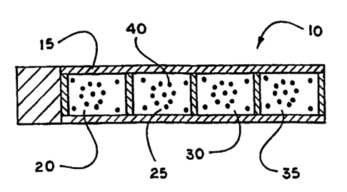
In another embodiment of the present invention, a
multiple analyte test is constructed on the same support. As
shown in Figure 1, a strip 10, having a substrate 15, is provided with
several micro-contact printed films 20, 25, 30 and 35, each film
having a pattern 40 printed thereon. Each of the micro-contact printed
films 20, 25, 30 and 35 have a different receptor material that is
specific for different analytes. It can be seen that the present
invention can be formatted in any array with a variety of micro-
contact printed films thereby allowing the user of the biosensor
device of the present invention to detect the presence of multiple
analytes in a medium using a single test.
There are many possible supports for the analyte-specific
receptor layers. Simple physisorption can occur on many
materials, such as polystyrene glass, nylon, or others well known
to those of ordinary skill in the art. Preferred embodiments of
immobilizing the analyte-specific receptor layers have involved
covalent attachment, such as that possible between thiol or
16
CA 02353535 2001-05-30
WO 00/34781 PCT/US99/27671
disulfide-containing compounds and gold. Typically, a gold
coating, 5 to 2000 nm thick, is supported on a Si/Si02 wafer,
glass, or a polymer film. Optionally, titanium can be used to
serve as an adhesion promoter between gold and the support.
The analyte-specific receptor attaches to the gold surface during
contact printing or immersion from a solution. Preferably, the
support comprises a gold coating on a MYLAR film.
Figure 2 outlines the procedure used for microcontact
printing. An elastomeric stamp is used to transfer analyte-
specific receptor "ink" to a gold surface by contact; if the stamp
is patterned, a patterned analyte-specific receptor layer forms.
The stamp is fabricated by casting polydimethylsiloxane (PDMS)
on a master having the inverse of the desired pattern. Masters
are prepared using standard photolithographic techniques, or
constructed from existing materials having microscale surface
features.
In a preferred embodiment of a typical experimental
procedure, a photolithographically produced master is placed in a
glass or plastic Petri dish, and a 10:1 ratio (w:w) mixture of
SYLGARD silicone elastomer 184 and SYLGARD silicone
elastomer 184 curing agent (Dow Corning Corporation) is
poured over it. The elastomer is allowed to sit for approximately
minutes at room temperature and reduced pressure to degas,
then cured for at least 4 hours at 60 C, and gently peeled from
25 the master. "Inking" of the elastomeric stamp is accomplished
by exposing the stamp to a 0.1 to 10 M aqueous solution of
disulfide-derivatized antibody typically by placing the stamp face
down in the solution for 10 seconds to 10 minutes. The stamp
is allowed to dry, either under ambient conditions, or typically by
30 exposure to a stream of air or nitrogen gas. Following inking,
the stamp is applied to a gold surface. Light pressure is used to
ensure complete contact between the stamp and the surface.
After 1 second to 5 minutes, the stamp is then gently peeled
from the surface. Following removal of the stamp, the surface is
rinsed and dried. Alternatively, further derivatization of
unstamped areas can be accomplished, either by using a second
stamp or by exposing the entire surface with a different reagent.
17
CA 02353535 2008-01-16
Subsequently, exposure to a protein-blocking agent, such as
BSA or f3-casein, or any other agent well known in the art, can
also be done.
The elastomeric character of the stamp is important to the
success of the process: Polydimethylsiloxane (PDMS), when
cured, is sufficiently elastomeric to allow good conformal contact
of the stamp and the surface, even for surfaces with significant
relief; this contact is essential for efficient contact transfer of the
receptor to a gold film. The elastomeric properties of PDMS are
also important when the stamp is removed from the master: if
the stamp were rigid (as is the master) it would be difficult to
separate the stamp and master after curing without damaging
one of the two substrates. PDMS is also sufficiently rigid to
retain its shape, even for features with sub-micron dimension.
The stamp is durable in that the same stamp can be used over
200 times over a period of a year without significant degradation
in performance. Using a printing roll for the stamp could, allow
for a continuous printing operation. Alternatively, ink jet
printing of the desired pattern could also be done if capable of
producing the feature sizes needed for diffraction, for example _<
100 m.
A more detailed description of the methods and
compositions of the present invention follows.
Any plastic film is suitable for the present invention.
Preferably, the plastic film is also capable of having a metal
coating deposited thereon. These include, but are not limited to
polymers such as: polyethylene-terephthalate (e.g., MYLAR ),
acrylonilrile-butadiene-styrene, acrylonitrile-methyl acrylate
copolymer, cellophane, cellulosic polymers such as ethyl
cellulose, cellulose acetate, cellulose acetate butyrate, cellulose
propionate, cellulose triacetate, cellulose triacetate, polyethylene,
polyethylene - vinyl acetate copolymers, ionomers (ethylene
polymers) polyethylene-nylon copolymers, polypropylene,
methyl pentene polymers, polyvinyl fluoride, and aromatic
polysulfones. Preferably, the plastic film has an optical
transparency of greater than 80%. Other suitable plastics and
18
CA 02353535 2001-05-30
WO 00/34781 PCT/US99/27671
suppliers may be found, for example, in reference works such as
the Modern Plastics Encyclopedia (McGraw-Hill Publishing Co.,
New York 1923-1996).
In one embodiment of the invention, the polymer film has
a metal coating thereon and has an optical transparency of
between approximately 5% and 95%. A more desired optical
transparency for the plastic film used in the present invention is
between approximately 20% and 80%. In a desired embodiment
of the present invention, the polymer film has at least an
approximately 80% optical transparency, and the thickness of
the metal coating is such as to maintain an optical transparency
greater than about 60%, so that diffraction images can be
produced by transmitted light. This corresponds to a metal
coating thickness of about 10 nm. However, in other
embodiments of the invention, the gold thickness may be
between approximately 1 nm and 1000 nm; for example,
thicker gold coatings (>20 nm) would still be suitable for
producing diffraction images by reflected light.
The preferred metal for deposition on the film is gold.
However, silver, aluminum, chromium, copper, iron, zirconium,
platinum and nickel, as well as oxides of these metals, may be
used.
In principle, any surface with corrugations of appropriate
size could be used as masters. The process of microcontact
printing starts with an appropriate relief structure, from which an
elastomeric stamp is cast. This `master' template may be
generated photolithographically, or by other procedures, such as
commercially available diffraction gratings. In one embodiment,
the stamp may be made from polydimethylsiloxane.
The stamp may be applied in air, or under a fluid capable
of preventing excess diffusion of the receptor material. For
large-scale or continuous printing processes, it is most desirable
to print in air.
In one embodiment of the present invention, the pattern is
formed on the metalized plastic polymer with the analyte-specific
receptor layer. After the stamping process, the metalized areas
19
CA 02353535 2001-05-30
WO 00/34781 PCTIUS99/27671
on the plastic may optionally be blocked, for example, with a
protein-repelling agent such as (3-casein.
This invention is further illustrated by the following
examples, which are not to be construed in any way as imposing
limitations upon the scope thereof. On the contrary, it is to be
clearly understood that resort may be had to various other
embodiments, modifications, and equivalents thereof, which, after
reading the description herein, may suggest themselves to those
skilled in the art without departing from the spirit of the present
invention.
EXAMPLES
EXAMPLE 1
Antibody-conjugated polystyrene particles were produced
by carbodiimide coupling with
ethyldimethylaminodicarbodiimide (EDAC, bottle #3 of
Polysciences kit, Catalog # 19539). For this example, 0.125 mL
of -a 10% suspension of 0.5 micron diameter blue carboxylated
particles (Bangs Laboratories, Fishers, Indiana, Cat
#D0005070CB) were activated with an aqueous solution of the
EDAC for 1-4 hours, rinsed, then exposed to 300 micrograms of
a monoclonal antibody to luteinizing hormone, alpha subunit,
(Fitzgerald Industries, Concord, Massachusetts, Cat# 10-L10,
Clone # M94136). The particles were again rinsed, blocked with
bovine serum albumin, and stored at 2.5% concentration in
phosphate buffered saline.
Next, a gold/MYLAR film was pre-treated (or blocked)
with a 5 mg/mL beta casein solution for 10 minutes, then
thoroughly rinsed and dried under an air stream. A PDMS
stamp of 10-micron circles was coated with thiolated antibody by
placing the stamp face down in a 0.5 mg/mL thiolated antibody
solution and soaking for 10 minutes. A strong air stream was
used to thoroughly dry the surface of the stamp. The coated
stamp was placed in contact with the gold/MYLAR film for 5
CA 02353535 2001-05-30
WO 00/34781 PCT/US99/27671
minutes, then removed. The resulting printed gold/MYLAR
film was rinsed in distilled water, and dried.
A 10 mM stock solution of the Sulfo-LC-SPDP is
prepared by dissolving 1.3 mg Sulfo-LC-SPDP into 2.07 ml de-
ionized water. The conjugation reaction is carried out in
phosphate buffered saline (PBS) containing 20 mM sodium
phosphate buffer, 150 mM NaCl, 1mM EDTA and 0.02%
sodium azide at pH 7.5. One milligram of lyophilized antibody is
dissolved in 450 ml PBS, and 50 ml of Sulfo-LC-SPDP stock
solution is added to the antibody solution. The mixture is
allowed to react at room temperature for 60 minutes. The
sample is applied to a 5 ml desalting polyacrylamide column
previously equilibrated with 5 bed volumes (25 ml) of PBS.
Fractions are eluted using PBS as the elution buffer, and the
protein in the fractions is monitored using a COOMASSIE
Protein Assay (Pierce Chemical Co). Typically, 50 ul of the
COOMASSIE reagent is mixed with 50 ul of each fraction in a
micro-titer plate. The COOMASSIE Blue substrate reacts with
the protein, producing a blue color, the intensity of which is
dependent upon the amount of protein present in the fraction.
The fractions which produce the most intense blue color are
those containing the majority of the protein eluted. These
fractions are pooled together to produce the disulfide form of the
final derivatized product. This is typically the form used for
contact printing.
Optionally, the disulfide-pyridyl group present on the
disulfide form of the thiolated binder can be reduced to a thiol
group in a reduction reaction. Instead of desalting on a column
equilibrated with PBS, the derivatized protein is desalted on a
column equilibrated with an acetate buffer (100 mM sodium
acetate buffer, 100 mM NaCl, pH 4.5). The acidic pH of this
acetate buffer acts to protect any disulfide bonds present on the
native protein from undesired reduction. In the reduction
reaction, 12 mg of dithiothreitol (DTT) is dissolved in 500 ml
acetate buffer and added to 1 ml of the SPDP derivatized
protein. The reaction mixture is incubated for 30 minutes at
room temperature, and desalted on a 5 ml desalting column
21
CA 02353535 2001-05-30
WO 00/34781 PCT/US99/27671
equilibrated with 5 bed volumes (25 ml) of acetate buffer. The
protein content of the fractions eluted is again monitored.by the
COOMASSIE Protein Assay as described above, and the
fractions containing the greatest amount of protein are pooled.
Both the disulfide and reduced forms of the thiolated
binders are stored in aqueous solution at 4 C until used for
contact printing.
The sensors were then used to detect an analyte. The
analyte solution was then mixed with microparticles (typically
50-70 microliters of analyte solution in 1 % bovine serum
albumin with 10-25 microliters of 1.5-2.5% particle suspension;
preferably, there is a 50:25 ratio of analyte solution to particle
suspension), and placed on top of a 1 cm square sensor sample.
After 5 minutes, a nitrocellulose disk (5 or 8 micron pore size,
Sigma #N3771 or N4146) with a small hole (e.g. 3/16") punched
out of the center was placed on top of the sensor. The disk was
used to wick away excess fluid and unbound microparticles. At
this time, a point light source was transmitted through the sensor
sample (using the small hole in the nitrocellulose). A diffraction
image would be seen on the other side of the light beam in the
presence of the target analyte.
As seen in Figure 4, SEM photomicrographs showed the
patterned placement of the microparticles.
EXAMPLE 2
A PDMS stamp of an x,y array of 10-micron circles was
"inked" with thiolated 30-mer oligonucleotide which is
complementary to the target DNA strand ("30-mer"; base
sequence of thiol spacer-5'-
CAATCCACGTCACGGACAGGGTGAGGAAGA-3' made by
Genosys, Inc., The Woodlands, Texas) by placing the stamp face
down with weight in oven-dried (50 C, vacuum) mixture of the
30-mer and ethyl acetate on glass. After 10 minutes, the inked
stamp was removed. At the same time, a gold/MYLAR film
was pre-heated on a 60 C hot plate for 5 minutes. Printing was
done by placing the inked PDMS stamp on top of the gold-
coated side of MYLAR at 60 C; weight and heat were
22
CA 02353535 2001-05-30
WO 00/34781 PCT/US99/27671
maintained during the 5 minute contact time. At this point, the
stamp was removed and the printed gold/MYLAR film was
washed with distilled water, and air-dried. The gold/MYLAR
film sample was then blocked with a 2.5 mg/mL beta casein
solution (in phosphate buffered saline, pH 7.2) for 10 minutes,
and rinsed with distilled water and air-dried.
These sensors were used to test for target DNA.
Hybridization of the target DNA to the capture DNA patterned
on the sensor surface took place as follows: A pre-heated
analyte solution (60 C water bath, 2 minutes) containing a DNA
strand of interest (a biotinylated 70-mer from Genosys with base
sequence of biotin-5' -
GGTAGACCGGAGAGCTGTGTCACCATGTGGGTCCCGGT
TGTCTTCCTCACCCTGTCCGTGACGTGGATTG-3') was
added to a pre-heated sensor (60 C hot plate, 5 minutes) and
then 75 microliters was added to an approximately 1 cm square
sensor for an additional 10 minutes heating. After this time, the
sensor sample was rinsed with water, and air-dried for
subsequent testing with microparticles. One variation to this
method is that the analyte solution, e.g., during a PCR
amplification, and the microparticles are exposed to the sensor at
the same time.
Next, Streptavidin-coated, 1 micron diameter particles
from Bangs Laboratories (Catalog # CPO1N) were added in 20-
30 microliter amounts, concentration of 2.4x10" particles per
mL, to the sensor. The sensor and particles were heated on a 60
C hot plate for 10 minutes (covered, while ensuring that
complete evaporation did not take place), and then rinsed gently
with distilled water. After this, a point light source was
transmitted through the sensor sample. A diffraction image
would be seen on the other side of the light beam in the presence
of the DNA analyte.
SEM photomicrographs show the patterned placement of
the microparticles.
23
CA 02353535 2001-05-30
WO 00/34781 PCT/US99/27671
EXAMPLE 3
Antibody-conjugated polystyrene particles were produced
by carbodiimide coupling with
ethyldimethylaminodicarbodiimide ("EDAC", bottle #3 of
Polysciences kit, Catalog # 19539). For example, 0.125 mL of a
10% suspension of 0.3 micron diameter blue carboxylated
particles (Bangs Laboratories, Cat #DC02/1836) were activated
with an aqueous solution of the EDAC for 1-4 hours, rinsed,
then exposed to 300 micrograms of a polyclonal antibody to IgE
(Fitzgerald Industries, Cat#20-IR77). The particles were again
rinsed, blocked with bovine serum albumin, and stored at 1.7%
concentration in phosphate buffered saline.
Next, a gold/MYLAR film was pre-treated (or blocked)
with a 5 mg/mL beta casein solution for 10 minutes, then
thoroughly rinsed and dried under an air stream. A PDMS
stamp of an x,y array of 10-micron diameter circles was coated
with thiolated antibody (antibody was initially Fitzgerald Catalog
#10-110 then derivatized or "thiolated" using Sulfo-LC-SPDP
by Pierce) by placing the stamp face down in a 0.5 mg/mL
thiolated antibody solution and soaking for 10 minutes. A
strong air stream was used to thoroughly dry the surface of the
stamp. The coated stamp was placed in contact with the
gold/MYLAR film for 5 minutes, then removed. The resulting
printed gold/MYLAR film was rinsed in distilled water, and
dried.
The analyte solution was then mixed with microparticles
(typically 50-70 microliters of analyte solution in 1 % bovine
serum albumin with 10-25 microliters of 1.5-2.5% particle
suspension; preferably, there is a 50:25 ratio of analyte solution
to particle suspension), and placed on top of a 1 cm square
sensor sample. After 5-10 minutes, a nitrocellulose disk (5 or 8
micron pore size, Sigma #N3771 or N4146) with a small (e.g.,
3/16" diameter) hole punched out of the center is placed on top
of the sensor. The disk was used to wick away excess fluid and
unbound microparticles. At this time, a point light source was
transmitted through the sensor sample by taking advantage of
the small hole in the nitrocellulose. A high order diffraction
24
CA 02353535 2001-05-30
WO 00/34781 PCT/US99/27671
image was seen on the other side of the light beam, signifying
the presence of the analyte.
EXAMPLE 4
A gold/MYLAR film was pre-treated (or blocked) with
a 5 mg/mL beta casein solution in phosphate buffered saline (pH
7.2) for 10 minutes, then thoroughly rinsed and dried under an
air stream. A PDMS stamp of 10-micron circles was coated
with thiolated antibody (e.g., rabbit anti-Candida albicans, Cat #
20-CRO4 from Fitzgerald Industries, Inc.) by placing the stamp
face down in a 0.5 mg/mL thiolated antibody solution and
soaking for 10 minutes. A strong air stream was used to
thoroughly dry the surface of the stamp. The coated stamp was
placed in contact with the gold/MYLAR film for 2 minutes,
then removed. The resulting printed gold/MYLAR film was
rinsed in distilled water, and dried.
The sensor sample was exposed to a 10% dilution in
phospate buffered saline, pH 7.2 of 40 nm gold particles coated
with goat anti-rabbit IgG (gold conjugate was from Polysciences,
Catalog # 22705). After one hour, the samples were thoroughly
rinsed with distilled water and dried under a nitrogen or air
stream. At this point, the samples do not diffract a HeNe laser
beam.
The samples were then exposed to silver enhancing
reagents from BBI (either BBI International's kit # SEKL 15
(Batch #2575) or large kit # SEKB250 (Batch #2484) were
used). A 1:1 v/v ratio of the enhancer and initiator reagents in
the kit were pre-mixed and then immediately placed on top of
the gold-particle coated samples. After 10-20 minutes exposure
(preferably, 10 minutes), the samples were rinsed with water,
dried, and examined. At this point, the samples diffracted light
(either a laser beam or a point white light source) most likely due
to the larger size of the silver nucleated around the gold
nanoparticles.
CA 02353535 2001-05-30
WO 00/34781 PCT/US99/27671
EXAMPLE 5
Samples prepared as per Examples 1 or 4 could also be
developed into a diffraction image by exposing it to an enzyme-
conjugate secondary antibody in the presence of the analyte,
such that if the analyte is present the secondary antibody would
bind and cause subsequent precipitate development with a
precipitating substrate specific to the enzyme.
A gold/MYLAR film was pre-treated (or blocked) with
a 5 mg/mL beta casein solution in phosphate buffered saline (pH
- 7.2) for 10 minutes, then thoroughly rinsed and dried under an
air stream. A PDMS stamp of 10-micron circles was coated
with thiolated antibody (e.g., mouse anti-luteinizing hormone
beta, Cat # 10-L15 from Fitzgerald Industries, Inc.) by placing
the stamp face down in a - 0.3 mg/mL thiolated antibody
solution and soaking for 10 minutes. A strong air stream was
used to thoroughly dry the surface of the stamp. The coated
stamp was placed in contact with the gold/MYLAR film for 5
minutes, then removed. The resulting printed gold/MYLAR
film was rinsed in distilled water, and dried.
The sensor sample was exposed to an analyte solution of
luteinizing hormone (Cat # 30-AL15 from Fitzgerald Industries,
Inc.) in 1% bovine serum albumin, phosphate buffered saline.
Concentration of antigen was varied from 0.1 to 1000 ng / mL.
After one hour at room temperature, the sample was rinsed with
0.02% TWEEN 20 solution, then distilled water. A subsequent
exposure to a secondary antibody (Fitzgerald Catalog # 61-L05
diluted 1:100 in distilled water) for one hour was done, followed
by rinsing as above. A TMB membrane enhancer solution (e.g.,
a 10:1 v/v mixture of Kirkegaard and Perry Laboratories'
reagents Cat #50-76-18 and Cat#50-77-01) was placed on the
sample for 10 minutes to cause development of a blue precipitate
in the circles or features. This precipitate caused a diffraction
image to form upon irradiation with a point light source.
26