Note: Descriptions are shown in the official language in which they were submitted.
CA 02353744 2001-07-24
. CP Dragone 65 1
N x N CROSSCONNECT SWITCH USING WAVELENGTH ROUTERS
AND SPACE SWITCHES
TECHNICAL FIELD OF THE INVENTION
The present invention relates to optical crossconnect switches and, more
particularly, to an N x N crossconnect switch implemented using wavelength
routers
combined with space switches.
BACKGROUND OF THE INVENTION
In high capacity optical networks, an essential device is the N x N
crossconnect
switch. The function of this device is to provide, at eaclh node, full
connectivity among
to several incoming fibers, each carrying several wavelength channels. The
switch must
be nonblocking, and it must be fast and efficient. If N is not too large,
these properties
can be realized by using a single N x N wavelength rout:er combined with
tunable
transmitters capable of producing N wavelengths. HowE;ver, this technique is
only
feasible if the size N of the router is not too large. This is because as N
increased, the
N x N router was difficult to realize in integrated form with satisfactory
performance of
low loss and low crosstalk, and each transmitter had to provide N wavelengths.
With the ever-increasing capacity of optical networks there is continuing need
for even larger N x N crossconnect switches.
SUMMARY OF THE INVENTION
2o In accordance with the apparatus of the present invention, the problem of
implementing a N x N crossconnect switch, for large N, is solved by using an
arrangement of smaller wavelength routers combined with space switches. In the
prior
art, a large N x N switch implemented using a rou~ter was difficult to realize
in
integrated form, with satisfactory performance of low loss and low crosstalk,
and each
transmitter had to provide N wavelengths. According to the present invention,
the
number of router wavelengths is reduced by a factor m and the N x N
crossconnect
switch is constructed in three stages using space switches and smaller
routers. The
input and output space switches can be implemented using crossbar or Clos type
CA 02353744 2003-11-04
2
construction. In the crossbar construction, the input and output switches are
1 x2 and 2x 1
switches respectively. In the Clos construction, the input stage uses m x (2m-
1) space
switches and the output stage uses (2m-1) x m space switches. In both the
crossbar or
Clos type construction, the reduced size of the center stage, using (Nlm) x
(Nlm)
wavelength routers, allows efficient realization in integrated form. Using
input space
switches with tunable transmitters, each with Nlm wavelengths, provides full
non-blocking connectivity of the NxN crossconnect switch. In one arrangement,
the input
and output space switches are implemented using 2x2, 1 x2, and 2x 1 switch
elements. In
one input space switch embodiment, a data modulator is combined with the 2x2
switch
1 o elements and integrated on a single wafer. Each input and output space
switch can be
realized with negligible crosstalk by using a dilated arrangement.
More particularly, the invention is directed to an N x N nonblocking optical
switch
for providing a connection between any of N inlets and any of N outlets, the N
x N switch
comprising:
an input stage including a plurality of input space switches, each input of
each of
the input space switches connects to a different one of the N inlets;
an output stage including a plurality of output space switches, each output of
each
of the output space switches connects to a different one of the N outlets; and
a center stage connected between the input stage and the output stage, the
center
2o stage including a plurality of Nlm x Nlm wavelength routers, wherein a
connecting link is
provided between each Nlm x Nlm wavelength router and each input or output
switch, so
that each Nlm x Nlm wavelength router connects to each input space switch and
each
output switch.
In accordance with one aspect of the present invention there is provided an N
x N
non blocking optical switch for providing a connection between any of N inlets
and any
of N outlets, where N is an integer, the N x N switch comprising: an input
stage including
a plurality of input space switches, each input port of each of the input
space switches
connects to a different one of the N inlets; an output stage including a
plurality of output
space switches, each output port of each of the output space switches connects
to a
3o different one of the N outlets; a center stage connected between the input
stage and the
CA 02353744 2003-11-04
2a
output stage, the center stage including a plurality of Nlm x Nlm wavelength
routers, m
being an integer divisor of N, wherein different inputs of each router are
connected to
different input switches, different outputs of each router are connected to
different output
switches, and the input and output stages allow any idle input port of an
input switch, and
any idle output port of an output switch, to be simultaneously connected to at
least one of
the routers, without disturbing existing connections; and wherein a signal
received at an
input port of the input stage is sent from that input stage using a wavelength
that is not
changed in its passage through the center stage to the output stage.
BRIEF DESCRIPTION OF THE DRAWINGS
Fig. 1 shows a prior art wavelength router consisting of a waveguide grating
between two free-space regions. The input and output waveguides are spaced by
a along
the input and output boundaries of the router;
CA 02353744 2001-07-24
CP Dragone 65 3
Fig. 2 shows a nonblocking cross-connect switch consisting of a N x N
wavelength routes combined with N tunable lasers, N modulators and N
receivers;
Fig. 3 shows a nonblocking cross-connect switch realized in three stages using
a
crossbax construction. The building blocks in the central stage are Nl2 xNl2
routers;
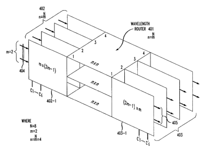
Fig. 4a shows an illustrative physical embodimf;nt, and Fig. 4b a block
diagram,
of the invention using a nonblocking N x N cross-connect switch realized using
Clos
arrangement. The building blocks in the center stags a.re n x n routers and,
in the other
two stages, m x (2m-1) and (2m -1) x m space switches;
Fig. 4c shows a routes reduction factor of 4, vrhere each center stage block
of
1o Fig. 4b is realized by using 2x2 routers in an arrangement similar to that
shown in Fig.
3;
Fig. 4d shows an arrangement, having a routes reduction factor of 4, which is
derived from Clos arrangement of Fig. 4b for N--16 and m=2 by realizing each
center
stage block of Fig. 4b using the Fig. 3 arrangement of lN/4 x Nl4 routers;
Fig. 4e shows an arrangement, having a routes reduction factor of 4, which is
derived from Clos arrangement of Fig. 4b where each center stage block of Fig.
4b is
itself implemented by a Fig. 4b arrangement;
Fig. 4f shows a mxp switch consisting of two stages of m,xp, and m2xp2
switches. Notice that m = m,mz and p plpz;
2o Fig. 4g shows the arrangement of Fig. 4f with each building block realized
using
the fully dilated 2x3 arrangement of Fig. 7;
Fig. 4h shows the arrangement of Fig. 4g with reduced depth and reduced switch
element count obtained by removing redundant switch elements;
Fig. 5 shows a nonblocking 2x3 arrangement with minimum number of
elements;
Fig. 6 shows a nonblocking 3x5 arrangement with minimum number of
elements;
CA 02353744 2001-07-24
CP Dragone 65 4
Fig. 7 shows a crossbar input space switch having two 1 x2 input switches, two
intermediate 1 x2 switches, and three 2x 1 output switchf;s;
Fig. 8 shows a crossbar input space switch of Fig. 7 as a combination of
binary
trees with two 1 x3 input switches and three 2x 1 output switches;
Fig. 9 shows a nonblocking 3x5 crossbar arrangement with minimum depth;
Fig. 10 shows a nonblocking 2x3 input space switch arrangement including two
input modulators; and
Fig. 11 shows a nonblocking 3 x2 output space switch arrangement including
two receivers.
1o In the following description, identical element designations in different
figures
represent identical elements. Additionally in the element designations, the
first digit
refers to the figure in which that element is first located (e.g., 102 is
first located in FIG.
1).
DETAILED DESCRIPTION
A nonblocking N x N switch is realized using wavelength routers as building
blocks. Each router [ 1,2] is a strictly nonblocking switch, which allows the
destination
of each input signal to be changed by simply changing the signal wavelength.
(Note in
this specification, a reference to another document is designated by a number
in
brackets to identify its location in a list of references found in the
Appendix B) With
2o reference to Fig. l, there is shown a prior art wavelength router
consisting of a
waveguide grating 101 between two free-space 'slab' regions, 102 and 103. The
input
and output waveguides are spaced by a along the input and output boundaries of
the
router and the waveguide grating arms 101 are spaced by b along the slab
regions. In a
well-known manner, changing the wavelength of a signal on any of the N input
waveguides changes to which of the N output waveguid~es the signal is
switched.
Shown in Fig. 2, is a nonblocking cross-connect switch consisting of a N x N
wavelength router of Fig. 1 combined with N tunable lasers 201, N modulators
202 and
N receivers 203. When N is not too large, the arrangement of Fig. 1 or Fig. 2
can be
CA 02353744 2001-07-24
CP Dragone 65
realized by using a single router. Then, each input signal must be produced by
a
multiwavelength laser capable of N wavelengths [ 1 ], and each input signal
can be
transmitted to any particular output port by simply selecting the appropriate
laser
wavelength. Thus, at any of the inputs I1 - IN, by changing the wavelength of
the
associated laser, the data signals Data-1 through Data-N can be switched to
any of the
outputs O1 - ON. Illustratively, the Data-1 signal on input I1 is shown
switched to
output ON, while the Data-N signal is switched to output O1.
However for large values of N > 64, this type of cross-connect switches is
difficult to realize using this technique, as discussed in .Appendix A. This
is because
1o each laser would then have to be capable of a large nurriber of
wavelengths, and also
because the router would be difficult to realize in integrated form with
satisfactory
performance of low loss and low crosstalk for large N. In accordance with the
present
invention, this problem is solved for large N by realizin;~ the N x N switch
by using an
arrangement of smaller routers. To this purpose an arrangement of (Nlm) x
(Nlm)
wavelength routers is combined with input and output stages consisting of
space
switches as shown in Figs. 3 and 4a. In Fig. 3, the N x N switch arrangement
is
realized with minimum loss and crosstalk by using a crossbar construction[3].
On the
other hand, it may be desirable to reduce the number of routers by using a
Clos
arrangement[4], shown in Fig. 4a, in which case it is gen;~erally desirable to
reduce loss,
2o crosstalk and waveguides crossings must be minimized as shown here. A
property of
the Fig 3 and Fig. 4a arrangements is that each signal tr<~verses only one
router. As a
consequence, the prior art problems of constructing a large N x N switch are
eliminated, since the number of wavelengths is reduced by a factor m, and the
size of
each router is also reduced by the same factor.
1. Optimum arrangements
Returning to Fig. l, there is shown a NxN router [S-7] consisting of N input
waveguides, N output waveguides, two dielectric slabs 102 and 103, and a
waveguide
grating 101 connected between the two slabs. The input; and output waveguides
are
connected to the two slabs, and the waveguides (arms) of the grating 101
between the
CA 02353744 2001-07-24
CP Dragone 65 6
two slabs are characterized by a constant path-length di:Fference. As a
consequence
each transmission coefficient from a particular input wa.veguide to a
particular output
waveguide is essentially characterized by periodic behavior, with equally
spaced peaks,
and each peak is produced by a particular order of the grating.
Ideally one would like to realize a switch by using a single N x N wavelength
router characterized as in [5,7] by a comb of N wavelengths such that the
transmission
coefficient from any input port {waveguide) to any output port has a
transmission peak
at one of the above wavelengths. In reality, if the routes of [5] is designed
to produce
the above property for a particular input port, for instance the central port,
one finds that
1o the above property only approximately applies to the other ports. As a
consequence, it
is shown in Appendix A that the routes is afflicted by wavelength errors that
increase
with N. Because of these errors, some of the wavelengths of maximum
transmission
deviate from the above comb of N wavelengths. In order to keep the resulting
losses
below 1 dB, one must require
N < 36 100
GHz
GHz being the channel spacing in GHz. For instance, for a channel spacing of
50 GHz, one must require N<52. This value can be increased by a factor 1.25 by
modifying the routes, by widening its passband as in [6], but this technique
also
increases loss and crosstalk by about 3dB.
2o The above restriction only arises because here we specify the same comb of
N
wavelength for all input ports. By allowing a different comb of wavelengths
for each
input port, the above restriction would be eliminated [2]~, but a total of N
different
combs (including a total of 2N I wavelengths) would then be required in order
to
provide maximum transmission from all input ports. This would make the
arrangement
more difficult to realize since each laser would have to produce a different
comb,
centered at a different wavelength.
The above considerations give one reason for which small values of N are
desirable in Fig. 1. As pointed out earlier, additional reasons are 1 ) that
it is generally
CA 02353744 2001-07-24
CP Dragone 65 7
desirable to simplify the laser design by reducing the number of wavelengths
required
from each laser and 2) that a router with large N > 64 is difficult to design
in integrated
form with satisfactory values of loss and crosstalk.
In view of the above difficulties it is advantageous for large N to realize
the
N x N switch by using, instead of a single N x N router, a combination of
smaller n x n
routers where n = Nlm and the reduction factor m is a suitable integer. Thus a
N x N
switch is realized in three stages, consisting of a central stage of n x n
routers combined
with input and output stages of nonblocking space switches as shown in Figs. 3
and 4. A
well-known property of these arrangements is that they are nonblocking in the
wide
to sense if the routers are replaced by nonblocking space switches, and a
large enough
number of such switches is used. Then, if any particular' input port and any
particular
output port are idle, one obtains the following nonblocking property: It is
possible to
simultaneously establish input and output paths from the above ports to a
particular
switch in the central stage without disturbing any of the other active paths.
That is, none
of the existing connections need be disturbed.
It should be noted that in the prior art, large N x N switch arrangements were
realized previously by using space switches, in which case their nonblocking
properties
are well known. Here, however, we use a combination of routers and switches in
which
case the nonblocking properties are only retained if no signal passes through
more than
one router. This condition is sufficient to insure that the signal can be
transferred to the
appropriate output port of the router by properly choosing the signal
wavelength.
Clearly one would like all routers to be characterized by the same comb of
wavelengths,
and the above conditions can be satisfied in Figs. 3,4 in different ways. The
simplest
and most important arrangements are obtained by using the constructions of
Figs. 3,4
with n x n routers characterized by n=Nlm, where m is a suitable reduction
factor. The
purpose of the input and output stages in this case is to 1?roduce the
appropriate
reduction factor m, and one finds that the two constructions of Figs. 3,4 have
different
advantages and disadvantages. For m=2, the crossbar construction of Fig. 3 is
attractive
for the simplicity of its input 301 and output 303 stages, and it has the
advantage of
CA 02353744 2001-07-24
CP Dragone 65 8
minimizing loss and crosstalk. As shown in Fig. 3, the central stages are
(N/2) x (N/2)
routers, i.e., 4 x 4, when N = 8 and m=2. Larger m can be realized by repeated
application of the same construction. For m=4, N = 16~, for instance, one can
replace
each (N/2) x (N/2) router in Fig. 3 with a crossbar arrangement of (N/4) x
(N/4) routers.
By this procedure, each switch in the central stage is realized by the same
construction
of Fig. 3, but with N replaced everywhere by Nl2. More generally, by repeated
application of the above construction, higher powers.of 2 for N can be
realized by
increasing the reduction factor m by factors of 2. Thus, for any N and m equal
to a
power of 2, the central stage consists of n x n routers with n = N/m and m=2S
where s is
to a suitable integer.
Shown in Fig. 4a is the physical arrangement of a Clos construction and Fig.
4b
shows the equivalent block diagram thereof. The Clos construction, e.g., Fig.
4a, has
the advantage, over the crossbar construction, e.g., Fig. 3, of requiring, for
m=2, only
three routers 401 instead of four. The Clos construction requires, however,
larger
building blocks for the input 402 and output 403 stages., as discussed later.
Clearly, by
repeated application of either construction, any power of 2 can be realized
for the
reduction factor m. As shown in Fig. 4a, for the generalized case, the number
of input
402 or output 403 switches, mx(2m-1) or (2m-1)xm, is equal to n=N/m, the
number of
n x n routers utilized is equal to (2m-1), where N is the number of input
ports and m is
2o the reduction factor. Thus, for the example shown in Fig. 4a, where N = 8,
m = 2, we
have n = 4 input 402 and output 403 switches and (2m-1 ) = 3 routers 401 of
size 4 x4.
As shown, each input switch is connected to each of the. 3 routers 401, and
therefore
either one of the m = 2 inputs 404 to an input switch, e.;g., 402-1, can be
switched to a
particular input, input 1, of each of the 3 routers 401. T'he control leads C
1. . . Ci to input
stage, e.g., 402-l, determine which input is switched to which router 401. At
each of
the 3 routers 401, the selection of wavelengths by the input stages 402
determines
which router input (inlet) is switched to which router output (outlet). At the
router
output side, the same respective output, e.g., output 1, of each of the 3
routers 401 is
CA 02353744 2001-07-24
CP Dragone 65 9
connected to a different input of one of the 4 output stages, e.g., 403-1. At
the output
stage, e.g., 403-1, only 2 signals are transmitted to outlc;ts 1 of the 3
routers 401 and
these two signals are switched to become the 2 outputs 405. Again the control
leads
C1...C'i to output stage, e.g., 403-l, determine which input is switched to
which output.
Note that the construction of the of input switches 402, mx(2m-1), is the
mirror image
of the output switches 403, (2m-1)xm.
In Figs.4a and 4b, changing the reduction factor m can change the size of the
routers and input and output stages. Thus, for a given lV, increasing m by a
factor of 2
reduces the size, n = N/m, of each router by a factor 2 and clearly this
technique can be
1o used with either the crossbar or Clos construction. As shown in Fig. 4c,
for instance, is a
switch arrangement where the router size used in each of the center stages 401
is further
reduced by a factor of 2, and hence implemented using N4 x Nl4 routers. Thus
Fig. 4c
illustrates a router reduction factor of 4, where each center stage block 401
of Fig. 4b is
realized by using 2x2 routers in an arrangement similar' to that shown in of
Fig. 3. In
Fig. 4c, the input stage 411 includes the 2x3 switches 402 and the 1 x2 switch
elements
413, the central stage includes the N4 xNl4 (i.e., 2x2) t~outers 410, and the
output stage
412 includes the 2x 1 switches 414 and the 3 x2 switch elements 403. Note that
while
Fig. 4b is a Clos construction (i.e., each input stage 402 can access each
center stage
router 401), the arrangement of Fig. 4c is a non-Clos arrangement.
Shown in Fig. 4d is a switch where N--16 and the reduction factor is m=4. In
Fig. 4d, the switch is realized by the arrangement of Fig. 4a, with each
building block
401 in the central stage realized by using the arrangemE;nt of Fig. 3 with N
replaced by
NI2. Then each central stage building block becomes a~ combination of 4 (N/4)
x (N14)
routers as shown in Fig. 4d. The resulting arrangement consists of a central
stage of 12
(N/4) x (N/4) routers 420. The twenty-four 1 x2 space :>witches 423 together
with the
eight 2x3 space switches 424 would then become the input stage 421. The twenty-
four
2x 1 space switches 425 together with the eight 3x2 space switches 426 would
then
become the output stage 422. In this arrangement each signal at one of the 16
inlets,
CA 02353744 2001-07-24
CP Dragone 65 10
427, is transferred by the input stage 421 to a particular (N/4) x (N/4)
router, 420, and
switched by the output stage to a particular one of the 16 outlets, 428.
Therefore by
properly choosing a signal wavelength, ~,1... 7~n, the signal at a switch
inlet 427 can be
switched via input stage 421 and router 420 to an appropriate outlet of the
router, using
a total of only n=NI4 wavelengths (4 in our example of N--16). Thus, each
input signal
laser (e.g., 1003 of Fig. 10) needs only to provide 4 wavelengths. At the
output side of
routers 420, the signal is then transferred by the output stage 422 to the
appropriate
switch outlet.
Shown in Fig. 4e is a Clos switch arrangement .derived from Fig. 4a where the
1o routers used in each of the blocks 401 of the center stake are further
reduced in size by a
factor of 2, and hence implemented using N4 xNl4 rou.ters. Note that Fig. 4e
is a Clos
construction since each switch inlet 43 l and outlet 437 can access each
center stage
router 432. Thus Fig. 4e illustrates a router reduction factor of 4, where
each center
block 401 is realized by using 2x2 routers in an arrangement similar to that
shown in of
Fig. 3. In Fig. 4e, the input stage 433 includes the switches 402 and 434, the
central
stage includes the N4 xNl4 routers 432, and the output stage 435 includes the
switches
436 and 403.
2. Clos Arrangement with Wavelength Routers in the central stage
As pointed out earlier Clos arrangement minimiizes the number of nxn
2o wavelength routers in the central stage. On the other hand, it requires
nonblocking
m x (2m -1) a.nd (2m-1) x m space switches in the input 402 and output 403
stages as
shown in Fig. 4a and, for this reason, the arrangement is found to have higher
loss and
higher crosstalk than the crossbar arrangement of Fig. :3. It is therefore
important to
optimize the input and output switches as shown next. Notice Fig. 4a requires
in
general 2m-1 routers and, in the special case m=2, it requires only three
routers. Since
m=2 is simplest to realize, and it can be used to realize any higher power of
2, it is the
most important case in practice, and each m x (2m-1) switch can then be
realized as in
Fig. 5 by using an arrangement of elements without wa.veguides crossings. With
CA 02353744 2001-07-24
CP Dragone 65 11
reference to Fig. 5, there is shown a nonblocking 2x3 arrangement implemented
with a
minimum number 3 of 2x2 switching elements. Each of the 2x2 switching elements
operate under control of a control signal C which controls whether the element
is in a
bar state, e.g., 501 and 503, or a cross state, e.g., 502. Note that none of
the
waveguides, e.g., 504, that interconnect the 3 elements 541 - 503 cross each
other.
Notice the 'depth' is generally defined as the total number of elements along
the path of
a particular signal, and it is an important parameter that determines loss and
crosstalk.
Thus, the depth of the 2x3 arrangement is two since a signal at an input port
must pass
through at most two elements to reach an output port.
to For m=3, on the other hand, one finds that a total of ten 2x2 elements is
required
and the optimum m x (2m -1) arrangement with minimum depth is shown in Fig. 6.
As
shown, 3 elements are used as 1x2 elements, 3 elements form a 3x2 arrangement,
and 4
elements form a 3 x3 arrangement. However, a disadvantage of Clos arrangement
of
Fig. 4a as compared to the crossbar arrangement of Fig. 3 is that it has
higher crosstalk.
Indeed, in Fig. 3, each input and output element receivf;s only one signal
and, as a
consequence, negligible crosstalk is caused by the eletr~ent extinction ratio.
In
comparison in Figs. S and 6, some of the elements, e.g., 501 and 503 of Fig. 5
simultaneously receive two signals, and appreciable crosstalk is then caused
by the
elements' extinction ratio. An attractive solution to this problem is to
modify the
2o arrangements of Figs. 5 and 6 so as to insure that each element is
traversed by only one
signal, e.g., like 502 of Fig. 5. We have derived for m==2 the arrangement of
Fig. 7,
which is referred to as a fully dilated 2x3 arrangement. This is the optimum
arrangement satisfying the above condition with minimum number of elements and
minimum depth. It is a crossbar arrangement of binary trees, and it consists
of two 1 x3
input switches (701,702 and 703,704 form separate 1x3 switches) combined with
three
2x 1 output switches, 705 - 707, as shown in Fig. 8. As. shown, the
arrangement
includes 7 elements, and it has only one waveguide crossing 708. Similarly for
m=3
the optimum m x (2m -1) dilated arrangement is realized with minimum depth, of
5, by
CA 02353744 2001-07-24
CP Dragone 65 12
using 22 elements forming a crossbar arrangement of input and output binary
trees, as
shown in Fig. 9. Three 2x2 elements 901 are used as 1x2 elements, 7 elements
form a
3x2 element 902, and 12 elements form a 3x3 element 903. Each 2x2 element in
the
above dilated arrangements is used as a 1 x2 or 2x 1 element, and hence it is
traversed by
only one signal, and therefore high extinction ratio is not required for the
various
elements. On the other hand, the arrangements of Figs. 5 and 6 are clearly
simpler, and
these are the preferred arrangements if the 2x2 elements have high extinction
ratios.
As previously noted, the depth is generally defined as the total number of
elements along the path of a particular signal, and it is an important
parameter that
1o determines loss and crosstalk. Also important in general is the depth given
by the total
number of columns formed by the various elements, since it determines the
wafer size
when the arrangement is realized integrated form a single wafer. The
arrangement of
Fig. 3 has the lowest depth. On the other hand, if only three routers are used
in the
central stage (Fig. 4a), then the arrangements of Figs 5 and 6 minimize depth,
number
of elements, and waveguides crossings.
As pointed out earlier, repeated application of Clos construction produces an
arrangement with reduction factor equal to the product of the individual
factors. For
instance two successive applications of Clos construction with factors ml and
m2
produce m=mime, and the result is an input stage arrangement similar to that
of Fig. 4b,
2o as shown in Fig. 4f. The only difference is that the input stage is now
made up ~f mxp
switches, instead of mx (2m-1) switches, and similarly i:he output stage
consists ofpxm
switches, with m=mime and p plp2 with pl= 2m1-1 andi. p2= 2m2-1. Each Fig. 4f
switch
now consists of two stages respectively made up of m, x pl and m2x p2
switches. The
input and output switches are now characterized by p>2,m-1 and, therefore, the
number
of center blocks can be reduced by realizing the NxN arrangement in a single
step, by
using the arrangement of Figure 4b with m=mlm2 and using mx (2m-1) and (2m-
1)xm
input and output switches. On the other hand simpler input and output switches
are
obtained by using the arrangement of Fig. 4d obtained with two applications of
Clos
CA 02353744 2001-07-24
CP Dragone 65 13
construction. In particular, from the arrangement of Fig. 4f, one can realize
for m=4 a
fully dilated arrangement with ml=m2=2 by using for each block in Fig. 4f the
arrangement of Fig. 7. In this case one finds that each connection 450 between
two
stages in Fig. 4f involves a 2x 1 element directly connecaed to a 1 x2
element, as shown
by 451 in Fig. 4g. Therefore each pair of elements 451 .of Fig. 4g can be
replaced by a
single 2x2 element 452 and the final result is the arrangement of Fig. 4h,
which is
attractive because it is simple to realize in integrated.form and it has
negligible first-
order crosstalk. Notice the above result, the occurrence for each connection
between
two blocks in Fig. 4f of a 2x 1 element directly connected to a 1 x2 element,
is a general
1o property of Fig. 4f whenever each building block is fully dilated. Then one
of the above
two elements 451 is redundant, and it can be removed provided the other is
replaced by
a 2x2 element.
As shown in Fig. 10, an attractive arrangement is obtained by including an
input
modulator in each of the m inputs. The m x(2m-I) element is shown to include a
modulator, 1001 and 1002, to modulate an input signal, I l and I2,
respectively, onto the
signal from lasers 1003 and 1004. The wavelength of lasers 1003 and 1004 are
selected
via a separate control signal C. Recall that the wavelength signal from lasers
1003 and
1004 determine the switching path of the input signals through routers 401 of
Fig. 4a.
Thus in Fig. 4a, the control signals C 1. . . Ci of the input: stage 402 and
control signals
2o C' 1... C'i of the output stage 403 together with the control signal C of
lasers 1003 and
1004 together determine the switching path for each input signal through the
NxN
switch of Fig. 4a.
Advantages of the above described Clos, Fig. 4, and Crossbar, Fig. 3,
arrangements over an arrangement using a single N x N router are 1) that only
ra laser
wavelengths are needed instead of N and that 2) each router can be realized in
integrated form with excellent performance in loss and efficiency. Indeed
using
existing technology, a 128 x 128 switch would be difficult to realize in a
single router.
CA 02353744 2001-07-24
CP Dragone 65 14
Notice the various n x n routers can be replaced by a conventional folded
arrangement
of a single grating combined with a lens or a reflector.
In summary, a large N x N switch is constructed in three stages, consisting
respectively of n x n wavelength routers combined with input and output stages
of space
switches. Each input switch is connected to a multiwavelength laser. The input
space
switch of Fig. 10 includes m modulators, to which m inputs and m
multiwavelength
laser signals connect, followed by a nonblocking m x m(2m-I) switch
arrangement of
2 x 2 switching elements. The resulting input space switch is suitable for
realization in
integrated form. Each input laser signal is first modulated by an input data
signal and
1o the switch then transfers it to a particular router, which transmits the
modulated signal
to a particular output port determined by the laser wavelength. In the output
space
switch shown in Fig. 1 l, an m x (2m-I) switch arrangement is followed by m
receivers.
In the simplest case, an N x N electronic switch is realized by using n =Nlm
input space
switches (of Fig. 10) and n =Nlm output space switches (of Fig. 11) in
addition to Zm-1
routers (401 of Fig. 4a).
What has been described is merely illustrative of the application of the
principles of the present invention. Other methods and arrangements can be
implemented by those skilled in the art without depari:ing from the spirit and
scope of
the present invention.
CA 02353744 2001-07-24
CP Dragone 65 15
APPENDIX A
Ideally one would like the router of Fig. 1 to be characterized by a set of N
wavelengths ~,~ such that the transmission coefficient from any input port to
any output
port has a transmission peak at one of the above wavelengths [1,5]. In
reality, if the
router is designed to produce the above property for a particular input port,
for instance
the central port, one finds that the above property only approximately applies
to the
other ports. As a consequence, the router is afflicted by wavelength errors
that increase
with N and, in order for these errors to be small, one must require
N<36 GHz
1o GHz is the channel spacing in GHz. For instance, for a channel spacing of
50
GHz one must require N<52. This value can be increased by a factor 1.25 by
modifying
the router, by widening its passband as in [6], but this technique also
increases loss and
crosstalk by about 3dB.
The router of Fig. 1 consists of N input waveguides, N output waveguides, two
dielectric slabs, and a waveguide grating connected between the two slabs. The
input
and output waveguides are connected to the two slabs with equal spacing a and
the
waveguides (arms) of the grating between the two slabs are characterized by a
constant
path-length difference. As a consequence each transmission coefficient from a
particular input waveguide to a particular output waveguide is essentially
characterized
2o by periodic behavior, with equally spaced peaks, and each peak is produced
by a
particular orderp of the grating. In particular, the wavelengths ~, of maximum
transmission from the i-th input waveguide to the output k-th waveguide are
specified
by the relation
xi -xk _ P~-Po~O (1)
R b
where the various parameters shown in Figure 1 are defined as follows:
x; , xk are the coordinates specifying the locations of the two
waveguides,
CA 02353744 2001-07-24
- CP Dragone 65 16
b is the spacing of the receiving and transmitting ends of the arms.
p0 is a particular orderp,
~,o is the central wavelength of maximum transmission for i = k and
P=Po
R is the radial distance of the input and output waveguides from the
central arm of the grating.
Notice in the above expression we can write
P~-Po~o =(P-Po)~o +Pot~-~o)+(P-Po)(~-~o)
where the last term can be neglected if either ~, -- ~,o or p - po is small.
By
to properly choosing the spacing a of the input and output waveguides so that
_1 R~,o
a=
N b
one obtains from the above expression (1) the wavelengths of maximum
transmission
~=~o+CJNkWP-Po)J po
t5 We choose among these wavelengths the particular subset ofNwavelengths ~,~
obtained for i=0, k j and p = po . This subset has an important property,
obtained
approximately by neglecting the last term of (2) so as to simplify Eq. (3)
simplifies to
~ Wo +~~ Nk WP-Po)' Po
According to this expression each transmission .coefficient has a peak at one
of
2o the above wavelengths ~,~ , and the appropriate values of j,p producing
each peak are
related in a simple way to i,k. On the other hand, the neglected term causes
the actual
wavelengths at the peaks corresponding to ~.~ to deviate from ~,~ . The errors
can be
reduced by a factor two by slightly displacing the output waveguides from
their initial
locations, and the maximum wavelength error is then given by
CA 02353744 2001-07-24
CP Dragone 65
Ss = ~'°
4Po
Then, by using a conventional (narrow band) design [6] one must require
N < 0.36po in order to keep the loss caused by t:he above error below 1 dB. In
the above expression po is determined by the channel spacing ~'° and
therefore we
Nopo
s obtain the final result
N<36 GHz
For instance, for a channel spacing of 50 GHz, vre must require N c 52. This
value can be increased by a factor 1.25 by widening the passband as in [6],
but this
technique also increases loss and crosstalk by about 3 d13. The above
restriction only
1o arises because we have specified the same comb of N wavelength for all
input ports. By
allowing a different comb of wavelengths for each input port, the above
restriction is
removed, but a total of N combs (including a total of 2N-1 wavelengths) is
then required
in order to provide maximum transmission from all input ports. Here we are
assuming
that each comb is produced by a multiwavelength laser. Therefore, since
different
15 lasers produce different combs, each laser is centered at a different
wavelength and the
arrangement becomes difficult to design. The above considerations give one
reason for
which small values of N are desirable in Figure 1. As pointed out in the
introduction,
additional reasons are 1) that it is generally desirable to ;>implify the
laser design by
reducing the number of wavelengths required from each laser and 2) that a
router with
20 large N > 64 is difficult to design in integrated form with satisfactory
values of loss and
crosstalk On the other hand, the neglected term causes the actual wavelengths
at the
peaks corresponding to ~,~ to deviate from ~,~ . The errors can be reduced by
a factor
two by slightly displacing the output waveguides from their initial locations,
and the
maximum wavelength error is then given by
25 s~ = ~o
4Po
CA 02353744 2001-07-24
CP Dragone 65 Ig
Then, by using a conventional (narrow band) design [6] one must require
N < 0.36po in order to keep the loss caused by the above error below 1 dB. In
the above expression po is determined by the channel spacing ~'o and therefore
we
NoPo
obtain the final result
N < 3 6 GHz
For instance, for a channel spacing of 50 GHz, we must require N < 52. This
value can
be increased by a factor 1.25 by widening the passband as in [6], but this
technique also
increases loss and crosstalk by about 3 dB. The above restriction only arises
because
we have specified the same comb of N wavelength for all input ports. By
allowing a
1o different comb of wavelengths for each input port, the above restriction is
removed, but
a total of N combs (including a total of 2N I wavelengths) is then required in
order to
provide maximum transmission from all input ports. Hare we are assuming that a
multiwavelength laser produces each comb. Therefore, since different lasers
produce
different combs, each laser is centered at a different wavelength and the
arrangement
15 becomes difficult to design. The above considerations give one reason for
which small
values of N are desirable in Figure 1. As pointed out in the introduction,
additional
reasons are 1) that it is generally desirable to simplify th.e laser design by
reducing the
number of wavelengths required from each laser and 2) that a router with large
N > 64
is difficult to design in integrated form with satisfactory values of loss and
crosstalk.
CA 02353744 2001-07-24
CP Dragone 65 19
APPENDIX B
REFERENCES:
[1] Doerr, C., Dragone, C., Glass, A., and Ka.minow, I. P., "A Broadband
Electronic N x N Cross-Connect Switch Using Tunable Lasers", U. S. Patent
s application, Serial No. 09/400,240, Filed on Sept 21, 1999.
[2) Bernasconi, P., Doerr, C. R., Dragone, C., Cappuzzo, M., Laskowski, E.,
and
Paunescu, A., "Large N x N Waveguide Grating Routers," Journal of Lightwave
Technology Systems," IEEE Communications Magazine, 18 (7): pp. 985-991, July
2000 May 1987.
[3] Padmanabhan, K., and Netravali, A., "Dilated Networks for Photonic
Switching,"
IEEE Transactions on Communications, Vol. C(JM-35, No. 12, pp. 1357-1365,
December 1987.
[4) Clos, C., "A Study of Non-blocking Switching Networks," B.S.T.J., 32,
1953, pp.
406-424.
[5] Dragone, C., "An N x N optical multiplexer using a planar arrangement of
two
star couplers," IEEE Photon. Technol. Lett., vol. 3, pp. 812-815, Sept. 1991.
[6] Dragone, C., "Efficient techniques for widening the passband of a
Wavelength
Router", IEEE Journal of Lightwave Technology, Vol. 16, No. 10, October 1998,
pp. 1895-1906. These techniques are also discussed in the three U. S. patents
filed
in 1994: Pat. No. 5,412,744, Pat. No. 5,467,418, Pat. No. 5,488,680.
[7] Dragone, C., "Optimum Design of a Planar Array of Tapered Waveguides," J.
Opt.
Soc. Amer. A., Vol. 7, No. 11, pp. 2081-2093, Nov. 1990, Applied Optics, 26,
April 1987.