Note: Descriptions are shown in the official language in which they were submitted.
CA 02353842 2001-06-07
Active Semiconductor Harlcnlanes
The present invention re3ates to active semiconductor backplanes suitable for
use with
a spaced opposed substrate. commonly a couaterelectmde, to form a cell, and to
devices comprising such backpIanes.
The device which is particularly described in this specification in connection
with a
preferred embodiment ~ is a spatial light modulator in the form of a smectic
liquid
crystal layer disposed between as active semiconductor backplane and a common
front electrode. It was developed in rnsponse to a requirement for a fast and,
if
possible, inexpensive, spatial light modulator comprising a relatively large
number of
1 o pixels with potential application not only as a display device, but also
for other forms
of optical processing such as correlation and holographic switching, Our
copendi,ng
International Patent Applications even filing and priority dates
(PCTlGB99104285,
ref-. .P20957W0, priority GB9827952.4; PCT/GB991a42$6 and PCT/GB99104276,
refs: f20958W0 and P20958W01, both priority GB9827965.6; PCT/GB99/04282,
15 ref: P20959W0, priority GB9827900.3; PCT/GB99144274, ref-. P20961 WO,
priority
GB9827964.9; PCTlGB99/04275, red P209b2WO, priority GH9827945.8; end
PCTIGB99/04250 and PCT/G899/04277, refs; P20963QV0 and P20963 WOI, both
priority GB 9827944.1) relate to other inyr~v~ ~p~~ associated with the
Spatial
liglit modulator.
2 0 During the course of development of the spatial moduletor, a series of
problems were
encountered and dealt with, and t3~e solutions to these problems (whether in
the form
of consbvction, ion or method) are net necessarily restricted in application
to the
embodiment, but will find other uses, Thus not all of the aspects of. the
present
invention are limited to liquid crystal devices, nor to spatial light
modulators.
25 Nevertheless, it is useful to commence with a discussion of the problems
encountered
in developing the embodiment to be described later.
The liquid crystal phase has been recognised since the last century, arid
there were a
few early attempts to utilise liquid crystal materials in light modulators,
none of
which gave rise to any significant successful commercial use. However, towards
the
30 end of the 1960's and in the 1970's, there was a renewed interest in the
use of liquid
crystal materials in light modulating, with increasing success as morn
materials, and
purer materials became available, and as technology in genera) pro~.essed.
I
,_,,,~~y'W F'cfW ,: .
. i.._ ?r.. ::Y j
CA 02353842 2001-06-07
WO 00/37999 - PCT/GB99/04279 .
Generally speaking, this latter period commenced with the use of nematic and
cholesteric liquid crystal materials. Cholesteric liquid crystal materials
found use as
sensors, principally for measuring temperature or indicating a temperature
change, but
also for responding to, for example, the presence of impurities. In such
cases, the
pitch of the cholesteric helix is sensitive to the parameter to be sensed and
correspondingly alters the wavelength at which there is selective reflection
of one
hand of circularly polarised light by the helix.
Attempts were also made to use cholesteric materials in electro-optic
modulators, but
during this period the main thrust of research in this area involved nematic
materials.
Initial devices used such effects as the nematic dynamic scattering effect,
and
increasingly sophisticated devices employing such properties as surface
induced
alignment, the effect on polarised light, and the co-orientation of elongate
dye
molecules or other elongate molecules/particles, came into being.
Some such devices used cells in which the nematic phase adopted a twisted
structure,
either by suitably arranging surface alignments or by incorporating optically
active
materials in the liquid crystal phase. There is a sense in which such
materials
resemble cholesteric materials, which are often regarded as a special foam of
the
nematic phase.
Initially, liquid crystal light modulators were in the form of a single cell
comprising a
2 0 Iayer of liquid crystal material sandwiched between opposed electrode
bearing plates,
at least one of the plates being transparent. The thickness of the liquid
crystal layer in
nematic cells is commonly around 20 to 100 microns, and there is a
correspondingly
small unit capacitance associated with a nematic liquid crystal cell.
Furthermore, the
switching time from a wholly "OFF" state to a wholly "ON' state tends to be
rather
2 5 long, commonly around a millisecond. Relaxation back to the "OFF" state
can be
somewhat longer, unless positively driven, but the "OFF" state is the only
stable one.
At the same time, electro-optic nematic devices comprising a plurality of
pixels were
being devised. Initially, these had the form of a common electrode on one side
of a
cell and a plurality of individually addressable passive electrodes on the
other side of
3 0 the cell (e.g. as in a seven-segment display), or, for higher numbers of
pixels,
intersecting passive electrode arrays on either side of the cell, for example
row and
2
CA 02353842 2001-06-07
WO 00/37999 - PC~'/GB99/04Z79 .
column electrodes which were scanned. While the latter arrangements provided
considerable versatility, there were problems associated with cross-talk
between
pixels.
The situation was exacerbated when analogue (grey scale) displays were
required by
analogue modulation of the applied voltage, since the optical response is non-
linearly
related to applied voltage. Addressing schemes became relatively complicated,
particularly if do balance was also required. Such considerations, in
association with
the relative slowness of switching of nematic cells, have made is difficult to
provide
real-time video images having a reasonable resolution.
Subsequently, active back-plane devices were produced. These comprise a back
plane comprising a plurality of active elements, such as transistors, for
energising
corresponding pixels. Two common forms are thin film transistor on
silica/glass
backplanes, and semiconductor backplanes. The active elements can be arranged
to
exercise some form of memory function, in which case addressing of the active
element can be accelerated compared to the time needed to address and switch
the
pixel, easing the problem of displaying at video frame rates.
Active backplanes are commonly provided in an arrangement very similar to a
dynamic random access memory (DRAM) or a static random access memory
(SRAM). At each one of a distributed array of addressable locations, a SRAM
type
2 0 active backplane comprises a memory cell including at least two coupled
transistors
arranged to have two stable states, so that the cell (and therefore the
associated liquid
crystal pixel) remains in the last switched state until a later addressing
step alters its
state. Each location electrically drives its associated liquid crystal pixel,
and is
bistable per se, i.e. without the pixel capacitance. Power to drive the pixel
to maintain
2 5 the existing switched state is obtained from busbars which also supply the
array of
SRAM locations. Addressing is normally performed from peripheral logic via
orthogonal sets (for example column and row) addressing lines.
In a DRAM type active backplane, a single active element (transistor) is
provided at
each location, and forms, together with the capacitance of the associated
liquid crystal
3 0 pixel, a charge storage cell. Thus in this case, and unlike a SRAM
backplane, the
liquid crystal pixels are an integral part of the DRAM of the backplane. There
is no
3
CA 02353842 2001-06-07
WO 00/37999 - PCT/GB99/04279 .
bistability associated with the location unless the liquid crystal pixel
itself is bistable,
and this is not normally the case so far as nematic pixels are concerned.
Instead,
reliance is placed on the active element providing a high impedance when it is
not
being addressed to prevent leakage of charge from the capacitance, and on
periodic
refreshing of the DRAM location.
Thin film transistor (TFT) backplanes comprise an array of thin film
transistors
distributed on a substrate (commonly transparent) over what can be a
considerable
area, with peripheral logic circuits for addressing the transistors, thereby
facilitating
the provision of large area pixellated devices which can be directly viewed.
l0 Nevertheless, there are problems associated with the yields of the
backplanes during
manufacture, and the length of the addressing conductors has a slowing effect
on the
scanning. When provided on a transparent substrate, such as of glass, TFT
arrays can
actually be located on the front or rear surface of a liquid crystal display
device.
In view of their overall size, the area of the TFT array occupied by the
transistors,
associated conductors and other electrical elements, e.g. capacitors is
relatively
insignificant. There is therefore no significant disadvantage in employing the
SRAM
configuration as opposed to the DRAM configuration. This sort of backplane
thus
overcomes many of the problems associated with slow switching times of liquid
crystal pixels.
2 0 Generally, the active elements in TFT backpLanes are diffusion transistors
and the like
as opposed to FETS, so that the associated impedances are relatively low and
associated charge leakage relatively high in the "OFF" state.
Semiconductor active backplanes are Limited in size to the size of
semiconductor
substrate available, and are not suited for direct viewing with no intervening
optics.
2 5 Nevertheless their very smallness aids speed of addressing of the active
elements.
This type of backplane commonly comprises FETs, for example MOSFETs or CMOS
circuitry, with associated relatively high impedances and relatively low
associated
charge leakage in the "OFF" state.
However, the smallness also means that the area of the overall light
modulation
3 0 (array) area occupied by the transistors, associated conductors and other
electrical
4
CA 02353842 2001-06-07
WO 00/37999 . PCT/GB99/04179
elements, e.g. capacitors can be relatively significant, particularly in the
SRAM type
which requires many more elements than the DRAM type. Being opaque to visible
light, a semiconductor backplane would provide the rear substrate of a light
modulator or display device.
In contrast to the type of RAM associated with computing, the pixel circuits,
and
more significantly the pixel transistors, are often at least partially exposed
to light.
This can lead to problems, especially with DRAM type backplanes where the
pixels
are part of the DRAM circuit, including photo-induced conductivity and charge
leakage.
Smec~ . c .iynia crystal Electro-Optic Cellc At a later period still,
substantial
development occurred in the use of smectic liquid crystals. These have
potential
advantages over nematic phases insofar as their switching speed is markedly
greater,
and with appropriate surface stabilisation the ferroelectric smectic C phases
should
provide devices having two stable alignment states, i.e. a memory function.
The thickness of the layer of liquid crystal material in such devices is
commonly
much smaller than in the corresponding nematic devices, normally being of the
order
of a few microns at most. In addition to altering the potential switching
speed, this
increases the unit capacitance of a pixel, easing the function of a DRAM
active
backplane in retaining a switched state at a pixel until the next address
occurs.
2 0 However, as the thickness of the liquid crystal approaches the thicknesses
associated
with the underlying structure of the backplane and with any possible
deformation of
the liquid crystal cell structure by flexing or other movement of the
substrates,
problems arise, for example as to the uniformity of response across the pixel
area, and
the capability for short circuiting across the cell thickness.
2 5 In the smectic liquid crystal phase, the molecules exhibit positional
order ("layers") in
addition to the orientational order exhibited by the cholesteric and nematic
phases.
There are a number of different smectic sub-phases which differ in the
orientational
order within the overall structure of the smectic layers, the most common
being the
smectic A phase (SmA) and the smectic C phase (SmC).
5
CA 02353842 2001-06-07
WO 00/37999 PCT/GB99/04279 .
The common alignment for smectic materials is planar (molecules generally
parallel
to the major cell surfaces) with the smectic layers nonmal to the plane of the
cell, as
this permits the field to be applied across the cell thickness. It is possible
to obtain
homeotropic alignment with the smectic layers in the cell plane, and such a
device
could provide a fast refractive index modulator. However, in order to apply
appropriate electric fields for switching, very small electrode gaps are
required and
therefore such devices tend to have very small active areas, and as a
consequence this
type of device is relatively uncommon.
In the smectic A phase the director is normal to the plane of the layers.
Application
of an electric field perpendicular to the director causes the latter to tilt
about an axis
parallel to the applied field by an amount approximately linearly dependent of
field
strength, making it possible to achieve analogue grey scale modulation.
Polarisation
of the light is affected, so that intensity or phase modulation may be
achieved, and
since the rotation of the director is in the plane of the cell, normally
incident light is
always perpendicular to the optic axis of the material. Coupled with the
thinness of
the cell, this leads to improved viewing angles for such devices. This effect,
called the
electroclinic effect, is extremely fast, switching times down to around 100
nano-
seconds having been observed.
In the smectic C phase, the director forms a constant ("tilt") angle with the
plane of
2 o the smectic layers. The tilt angle depends on the material and the
temperature, and
defines a cone with its tip on the smectic layer and its axis normal to the
layer, all
possible positions of the director lying on the cone surface. In the bulk of a
chiral
smectic C phase (SmC*) the director precesses from layer to layer as in a
helix.
In the chiral smectic C phase, liquid crystal materials are ferro-electric,
having a
2 5 permanent dipole, sometimes termed spontaneous polarisation (P~. In the
bulk
material, Ps rotates in the plane of the layer as the director precesses, so
no net effect
is observable. Bulk ferro-electricity can be observed if the precession is
suppressed,
either by surface stabilisation of the director positions such that only the
two
orientations of director which lie in the plane of the device are possible,
and/or by
3 0 back-doping with a chiral material of the opposite hand.
6
CA 02353842 2001-06-07
WO 00/37999 - PGT/GB99/04279 .
Smectic C* materials can be broadly divided into two classes known as high and
low
tilt materials respectively. Class I materials have the phase sequence
isotropic -
nemadc - smectic A* - smectic C*, and tend be low tilt materials, having tilt
angles
generally grouped up to around 22.5° (cone angle of 45°); class
II materials have the
phase sequence isotropic - nematic - smectic C*, and tend to be high tilt
materials
with greater tilt angles. Materials with a cone angle greater than 75°
are rare,
although for holographic applications, which require phase modulation, a cone
angle
of 90° would be ideal.
With low tilt materials, the smectic layers are inclined relative to the cell
surface
rather than at right angles, such that the director cone has a tilted axis and
its surface
is tangential to the cell surface. For high tilt materials the cone axis is
normal to the
cell surface.
When the structure is surface stabilised, then in theory, at least for Class I
materials
there is no preference between the two states of a low tilt material and a
bistable
structure should result. Surface stabilisation can be achieved simply by
making the
layer in the cell thin. The two states will have different effects on
polarised light, and
so can provide intensity or phase modulation. In practice, it is very
difficult or
impossible to obtain true bistability, especially on silicon backplanes and
there will a
slight preference for one state over the other. Nevertheless, this should give
rise to
2 0 relatively long relaxation times.
For high tilt materials, the two states are not equal, and one state is
preferred over the
other, so that there is monostability in the absence of any other factor. The
two states
are such that phase modulation of light may be obtained, and, indirectly,
intensity
modulation, e.g. in holographic applications. Both high and low tilt materials
may be
2 5 used in the spatial light modulator of the invention.
The presence of the spontaneous polarisation, and its
realignment as the liquid crystal molecules realign under the influence of an
electric
field, leads to a significant additional current or charge flow during
realignment, e.g.
between electrodes either side of a smectic layer. A pixel of area A will
consume a
3 o charge of 2AP, during switching. This factor is particularly important
when pixel
switching is controlled by a DRAM type of active backplane, when pixel
capacitance
7
CA 02353842 2001-06-07
WO 00/37999 - PCT/GB99/04279
and P, become important design parameters. It should also be noted that charge
consumption reduces the field across the electrodes in such devices if the
addressing
pulse is insufficiently long to accommodate pixel switching, as in the present
preferred embodiment.
As has already been noted, the use of the backplanes described herein is not
limited to
liquid crystal devices. However, these backplanes are particularly suited for
use in
the manufacture of liquid crystal devices. Again, although it is possible to
employ
nematic or cholesteric materials in such devices, it is preferred to employ
smectic
materials because of their faster switching action. Also, in the case of using
a DRAM
l0 type active backplane (this does not apply when the backplane is the SRAM
type
since power/current can be continuously applied to each pixel), the ability to
extend
the relaxation time, or even to obtain a bistable effect, once the pixel has
been placed
in the desired state.
One advantage of having a fast switching time in the case where relaxation
occurs lies
in the increase of the fraction of the pixel repeat address period usable for
viewing
time. Another advantage, particularly where optical processing is concerned is
the
increase in data throughput.
Pixel Strnctere - Switching and Addre._cs Ti-mec When using a SRAM type
backplane to switch a capacitive element the time necessary to address the
location on
2 o the backplane can be as small as is necessary to switch that location,
regardless of
whether the capacitive element has responded. The location is always coupled
to the
power supply, and can continue to supply power (current/voltage) to the
capacitive
element after the addressing pulse has ceased.
By contrast, power is supplied to a capacitive element from a DRAM location
only
2 5 while addressing is taking place, after which the active element
(transistor) is turned
off. If the addressing pulse is insufficiently long for transfer of the
requisite amount
of charge, the capacitive element is incompletely switched. This is likely to
occur, for
example, when the capacitive element includes ferroelectric material, as in
some
smectic liquid crystal cells, and the addressing time is short, for example in
a large
3 0 scale array.
8
CA 02353842 2001-06-07
Ono solution is to provide an additional "slug" capacitance which is rapidly
charged
during the addressing pulse and so can provide a reservoir of charge whi3e the
capacitive clement switches over a longer time period.
In a first aspect the invention provides a semiconductor active baclcplane
including an
array of addressable active elements on a semiconductor substrate for
selectively
energising respective first electrodes of the array, wherein at least part of
the region
beneath a said first electrode is formed as a depletion region whereby in use
it acts as
a reverse biassed eapacitative diode characterised in that at least one charge
trapping
implant is provided adjacent but spaced from said depletion region.
In a second closely related aspect the invention provides a semiconductor
active
backplane including an array of addressable active elements on a semiconductor
substrate for selectively energising respecdive first electrodes of the array,
wherein at
least part of the region beneath a said first electrode is formed as a
depletion region
whereby in use it acts as a reverse biassed capacitative diode characterised
in that a
guard ring is provided over or around the periphery of said depletion region
to prevent
or hinder charge carriers from crossing between the depletion region and the
rust of
the substrate.
In a third aspect the invention provides a senvconductor active backplane
including
an array of addressable active elements on a semiconductor substrate for
selectively .
energising respective first electrodes of the army, characterised in that at
least pert of
the region beneath a said first electrode is provided by individual capacitor
plaits
formed beneath the electrode, one coupled to the substrate and the other
coupled to
the electrode.
The first second and third aspects of the invention are particularly uxful
where ~e
2 5 active element comprises a single ~nsistor as in a DRAM type backplarie.
In US Patent 4,839,70? (Shields) part of a dielectric layer is employed as a
capacitivc
region between a source region and a silicon substrate. The dielectric layer
is
insulating, and the construction dots not involve two distinguislsable
capacitor plates
below the addressable electrode, one coetpled to the addressable electrode,
the other
3 0 co upled to the substrate, as in embodiments of t>te. present invention.
9
/;~~1.T.-~z:r~~_.tl ~~~~,:;~.._
::_~ .~..
CA 02353842 2001-06-07
WO 00/37999 - PCT/GB99/04Z79 _
In US Patent No 5,537,234 (Williams et al) trench capacitors are formed in the
rear
surface of a semiconductor layer, which layer is adhered to a substrate and
provides
transistors in an array. The capacitors lie below addressable electrodes but
they
neither comprise depletion regions, nor act as reverse biassed diodes.
Furthermore,
the construction involves only one plate, as opposed to two individual
electrodes, one
coupled to an addressable electrode and one coupled to the substrate.
Electrostatic Stabilisation Once the capacitive element has been switched, it
is
still necessary to maintain the element in its switched state, at least until
it is
energised again. Again SRAM type backplanes do this successfully by virtue of
their
continuous coupling to the power supply lines.
For DRAM type backplanes, it is necessary to note that the charge consumption
which occurs when a pixel is switched in one direction gives rise to a
corresponding
generation of charge when the pixel switches in the other direction.
Therefore, if a
switched pixel is completely electrically isolated, charge cannot flow and the
pixel
cannot relax. In operation of a DRAM type array, this may be effected by
turning off
all the transistors of the array, and in the preferred embodiment this is made
possible
by applying a global reset signal NRAR to the row scanners.
In practice, charge leakage cannot be completely eliminated, and so relaxation
will
occur, but over an extended period. A common cause of charge leakage is
2 0 photoconductivity associated with the slug capacitance mentioned earlier
and/or
photoconductive or other leakage currents in the associated switching
transistor of the
DRAM array. This is particularly marked with DRAM type backplanes for optical
use, where incident illumination can penetrate directly or indirectly to the
underlying
backplane structure, thereby causing photoconduction.
2 5 Electrical isolation is thus a useful but imperfect tool for prolonging
relaxation times.
It will be appreciated that whether a long relaxation time is achieved through
an
appropriate choice of material and cell design, or by electrical isolation,
the important
factor is that sufficient time can be allowed between successive addressings
of any
pixel for it to be maintained essentially in its desired state. Particularly
in the case of
CA 02353842 2001-06-07
DRAM type 6ackplanes it is important that the design is such that charge
leakage is
minimised.
'thus in a fourth aspxt the invention provides a senuconduetor active
backplane
including an array of addressable active eLrnents on a semiconductor substrate
far
energising rosp~ctive first electrodes, and fist and second orthogonal sets of
addressing conductors, a respective pair of addressing conductors, one from
each set,
being associated with the addressing of a corresponding active element,
characterised
in that substantially the whole of each active element is covered by a said
addressing
conductor in the form of a metallic conductor. In a fifth closely related
aspect,
~, 0 substantially the whole of each elctncnt is covered by a said pair of
addressing
conductors in the form of metallic conductors. In one embodi~ncnt of the fifth
aspect
the active element is sited below the crossover between row and column
conductors.
In all the above aspects of the invention where each said active element is
connected
to a metal electrode on said insulating layer, the array of said metal
electrodes thus
formed preferably covers more than 65%, and more preferably more than $0%, of
the
area of said array.
It may be possible to regard the type of rvnstruction of the certain aspects
of the
invention as being disclosed with respect to thin film transistor (TFT) array
active
backplanes; of which the following are exemplary disclosures - EP 0762184
{Sharp
2 0 KK); IrP 4708356 (Sony); EP 0603866 (Sony); EP OS42~79 {Sharp KK); US
5,777,703 (Nishikawa); US 5,691,782 (Nishikawa); US 5,4i 4,283 (den Boer).
Similarly EP 0877283 (Sanyo); EP 0793135 (Citiztn Watch); EP 0752611 {a1S
Qptical Imaging Sysuats, Inc); and EP 068575'7 (Matsushita) might be
considered
exemplary disclosures of thin fclm arrays in which an electrode is coveted by
as
2 S insulating film through which a connection is made to a larger reflective
conductor
over the insulating film.
Ncverthelessr there are very real differences between TFT arrays and active
semiconductor backplanes, not the least of which is that TFT arrays are much
larger
and transparent. It is believed that the effects of incident light on the
transistors or
3 0 other active elements in active semiconductor baekplanes from has not
heretofore
been considered or even~recognised, and that as a result no positive stops
have been
taken to protect such elements in the manners now pmpased.
11
~'.~~~i',:-::i_~ h': ..
CA 02353842 2001-06-07
WO 00/37999 - PC1'/GB99/04279
Further features and advantages of the invention can be derived from a
consideration
of the appended claims, to which the reader is referred, and of the following
description of an embodiment of the invention made with reference to the
accompanying drawings, in which:
Figure 1 shows in schematic cmss-sectional view a liquid crystal cell which
incorporates an active backplane and is mounted on a substrate;
Figure 2 is an exploded view of components of the liquid crystal cell of
Figure 1;
Figure 3 is a schematic plan view (floorplan) of the active backplane of the
liquid
crystal cell of Figure 1, including a central pixel array;
1 o Figure 4 is a schematic cross sectional view of part of the backplane of
Figure 3 to
illustrate the various layers and heights encountered in the region of the
pixel array;
Figure 5 is a schematic plan view of a single pixel of the array of the
backplane of
Figure 4; and
Figures 6 to 8 show modifications. of Figure 5.
Figure 1 shows in schematic cross-sectional view a liquid crystal cell 1
mounted on a
thick film alumina hybrid substrate or chip carrier 2. The cell 1 is shown in
exploded
view in Figure 2.
CeII 1 comprises an active silicon backplane 3 in which a central region is
formed to
provide an array 4 of active mirror pixel elements arranged in 320 columns and
240
2 o rows. Outside the array, but spaced from the edges of the backplane 3, is
a peripheral
glue seal 5, which seals the backplane 3 to the peripheral region of a front
electrode 6.
Figure 2 shows that the glue seal is broken to pemut insertion of the liquid
crystal
material into the assembled cell, after which the seal is completed, either by
more of
the same glue, or by any other suitable material or means known per se.
2 5 Front electrode 6 comprises a generally rectangular planar glass or silica
substrate 7
coated on its underside, facing the backplane 3, with a continuous
electrically
conducting silk screened indium-tin oxide layer 8. On one edge side of the
substrate
7 is provided an evaporated aluminium edge contact 9, which extends round the
edge
12
CA 02353842 2001-06-07
WO 00/37999 - PCT/GB99/04279
of the substrate and over a portion of the layer 8, thereby providing an
electrical
connection to the layer 8 in the assembled cell I.
Insulating spacers 25 formed on the silicon substrate of the backplane 3
extend
upwards to locate the front electrode 6 a predetermined, precise and stable
distance
from the silicon substrate, and liquid crystal material fills the space so
defined. As
described later, the spacers 25 and the backplane 3 are formed on the silicon
substrate
simultaneously with formation of the elements of the active backplane thereon,
using
all or at least some of the same steps.
Figure 3 shows a general schematic view of the layout ("floorplan") of the
active
backplane 3. As will be described in detail later with reference to Figures 4
to 8, each
one of the central array 4 of pixel active elements is composed essentially of
an
NMOS transistor having a gate connected to one of a set of a row conductors, a
drain
electrode connected to one of a set of column conductors and a source
electrode or
region which either is in the form of a mirror elcctrode or is connected to a
mirror
electrode. Together with an opposed portion of the common front electrode 6
and
interposed chiral smectic liquid crystal matcrial 20, the rear located mirror
electrode
forms a liquid crystal pixel cell which has capacitive characteristics.
Even and odd row conductors are connected to respective scanners 44, 45 spaced
either side of the array. Each scanner comprises a level shifter 44b, 45b
interposed
2 0 between a shift register 44a, 45a and the array. In use, a token signal is
passed along
the registers to enable (render the associated transistors conductive)
individual rows
in turn, and by suitable control of the registers different types of scan,
e.g. interlaced
or non-interlaced, can be performed as desired.
Even and odd column conductors are connected to respective drivers 42, 43
spaced
2 5 from the top and bottom of the array. Each driver comprises a 32 to 160
demultiplexer 42a, 43a feeding latches 42b, 43b, and a level shifter 42c, 43c
between
the latches and the column conductors. In use, under the control of a 5-phase
clock,
data from the memory 24 for successive sets of 32 odd or even column
conductors is
passed from sets of edge bonding pads 46, 47 to the demultiplexers 42a, 43a,
and
3 0 latched at 42b, 43b before being level shifted at 42c, 43c for supply as a
driving
voltage to the column conductors. Synchronisation between the row scanning and
13
CA 02353842 2001-06-07
WO 00/37999 - PCT/GB99/04279
column driving ensures that the appropriate data driving voltage is applied
via the
enabled transistors of a row to the liquid crystal pixels, and for this
purpose various
control circuits 48 and test circuits 48' are provided.
Subsequent disabling of that row places the transistors in a high impedance
state so
that charges corresponding to the data are then maintained on the capacitive
liquid
crystal pixels for an extended period, until the row is again addressed.
The gaps 21 between the level shifters 44b, 45b and the adjacent edges of the
array 4
are lmm wide, and the gaps 22 between the level shifters 44b, 45b and the
adjacent
edges of the array 4 are 2mm wide. These gaps, or glue lanes, are sufficiently
large to
1 o completely accommodate a glue seal 5 of approximate width of 300 microns
while
allowing for tolerances in positioning of the seal. As shown in Figure 1, the
sine of
the front electrode 6 sufficient to cover only the array and most of the glue
lanes. In
the embodiment the array is l lmm by 8 mm, and the front electrode is 12.4 mm
by
9.4 mm.
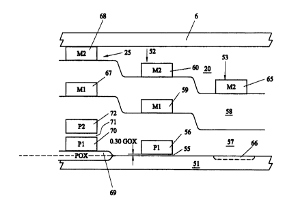
As schematically illustrated in Figure 4, the active backplane is based on a p-
type
silicon substrate 51. In the region of the array 4 it includes NMOS
transistors 52,
pixel mirrors 53 and the insulating spacer columns 25, and the substrate 51 is
covered
first by a lower substantially continuous silicon oxide layer 57 and then by
an upper
substantially continuous silicon oxide layer 58. It should be noted that
Figure 4 is
2 o included merely to illustrate the different heights encountered in the
backplane and
that the other spatial arrangements of the elements do not correspond to what
is found
in practice. Figure 5 shows a plan view of an actual arrangement of transistor
and
mirror electrode, generally similar to that of Figure 4, but with the column
25 not
shown. Transistors 52 are the highest part of the circuitry itself.
2 5 In addition to these layers, the transistor 52 is further defined by a
metallic gate
electrode 59 on the layer 57 and a metallic drain electrode 60 on layer 58.
Electrodes
59 and 60 are portions of a row conductor 61 and a column conductor 62
respectively
(see Figure 5). At the transistor 52, the layer 57 is modified to include a
polysilicon
region 56 spaced from the substrate 51 by a very thin gate oxide layer 55.
14
CA 02353842 2001-06-07
WO 00/37999 - PC=T/GB99/04279 _
The transistor source is in the form of a large diffusion region 63 within the
layer 58
which is connected to electrode 65 of the pixel mirror 53, with the gate
region 64
being located essentially under the crossover region of the column and row
conductors 61, 62 to maximise the fill factor and to protect it from incident
light.
The pixel mirror is formed by the pixel electrode 65 on layer 58, which
electrode is of
the same metal as, and formed simultaneously with, the drain electrode 60.
Beneath
most of the mirror electrode 65 there is formed an n-type depletion region 66
in the
substrate 51. In the assembled device, the pixel electrodes are spaced from
the
opposed front electrode 6 by somewhat less that 2 microns with smectic liquid
crystal
material 20 interposed.
The pixel mirror is essentially flat, since there are no underlying discrete
circuit
elements, and occupies a proportion (fill factor) of around 65% of the pixel
area. The
need to maximise the fill factor is one consideration in the decision to
employ a
DRAM type backplane, rather than the SRAM type in which more space needs to be
devoted to the two transistors and their associated elements.
The insulating column or pillar 25 which is associated with each pixel extends
above
the topology of the rest of the backplane, but is also composed of the layers
57, 58
over the substrate 51, with a first metal film 67 between the layers S7, 58
and a
second metal film 68 between layer 58 and (in use) the front electrode 22.
First and
2 0 second metal films 67, 68 are of the same metals, and deposited at the
same time, as
the electrodes 59, 60 of the transistor 52. In the region of the spacer, the
substrate is
modified to provide a field oxide layer 69, and the bottom of layer 57 is
modified to
provide two polysilicon layers 70, 72 spaced by a thin oxide layer 71.
Although it includes metallic layers, the spacer provides good insulation
between the
2 5 front electrode and the active backplane. By forming insulating spacers in
this
manner, it is possible to locate them accurately relative to other elements on
the
backplane, thereby avoiding any interference with optical or electrical
properties. By
creating them at the same time as the active and other elements of the
backplane,
using the same processes, there are advantages in terms of cost and
efficiency.
CA 02353842 2001-06-07
WO 00/37999 - PC~'/GB99/04279
As mentioned above, a pixel cell thus formed has capacitance. Chiral smectic
liquid
crystal materials are ferroelectric, so that application of an electric field
sufficient to
cause realignment of the molecules is associated with an additional transfer
of charge.
This effect is associated with a time constant insofar as the liquid crystal
material
takes time to realign.
The requirement for charge to flow during realignment, and the associated time
constant, have a number of consequences. In particular, while the realignment
can be
relatively fast, it may still be much less than is required for fast scanning
of the
device.
1 o With a SRAM type backplane, the state of a pixel is retained until the
next address,
and with power being supplied finm a bus current can be supplied until
realignment
has been completed. However, with a DRAM type backplane, power is supplied to
each pixel only during the addressing period. The capacitance of the cell is
relatively
small, and cannot retain sufficient charge for realignment to be completed.
One way of dealing with this problem is to provide each pixel with an
additional
"slug" capacitance which is quickly charged when the pixel is addressed, its
charge
thereafter being consumed as the liquid crystal molecules realign and
subsequent
pixels are being addressed. Thus the slug capacitance effectively avoids the
need for
an addressing pulse as long as the realignment time.
2 o In Figure 5, the diffusion layer 66 forms in use a reverse biassed diode,
the depletion
region of which acts as the slug capacitance. Figure 6 shows a variant in
which the
depletion layer 66 is substituted by a parallel plate capacitor formed between
two
polysilicon regions 80 (similar to regions 70 and 72 in the insulating column
of
Figure 5, and preferably formed therewith). The lower polysilicon region is
connected to the substrate 51 by a space consuming metal strap 81, so that
while this
arrangement has a similar capacitance to the reverse biassed diode, it
significantly
reduces the fill factor of the mirror electrode and for this reason is not
preferred.
The smectic liquid crystal used in the embodiment has a monostable alignment,
so
that for the DRAM type pixel element to remain in the switched state until it
is next
3 0 addressed, it is essential to limit charge leakage. In a sense, the fact
that there is an
16
CA 02353842 2001-06-07
WO 00/37999 - PCT/GB99/04279
additional charge displacement during realignment is helpful, in that the
amount of
charge leakage to permit relaxation to the original state is relatively large.
Unlike a conventional encapsulated computer DRAM, illuminating light can
penetrate to the backplane. If it reaches sensitive elements,
photoconductivity can
permit relaxation of the pixel in less time than the scanning period, and this
should
not be allowed to happen. Steps therefore need to be taken (a) to reduce light
penetration to sensitive elements as far as possible; and (b) to alleviate the
effects of
any light which nevertheless still penetrates.
In Figures 4 to 6, step (a) is implemented insofar as the transistor 52, and
particularly
its gate region, is located substantially beneath metallic conductors 60, 61
and in that
the diode provided by region 66, which is especially photosensitive, is
largely hidden
by the mirror layer 65. However, there are still gaps which allow light to
penetrate
directly or indirectly.
As implied above, there is particular concern relating to the diode region.
Thcre is
less concern when the slug capacitance is of the general form indicated in
Figure 8
but this has a lower fill factor.
Figure 7 shows a modification of the arrangement of Figure 5 in which n-type
charge
trapping implants 66a are formed in exposed areas of the silicon substrate
adjacent the
edges of the pixel mirror 53, thus preventing photo-induced carriers from
entering the
2 o depletion region 66.
Figure 8 illustrates an alternative modification in which an n-type guard ring
100 is
formed on the peripheral region of the diffusion region 66. While this is more
effective than the arrangement of Figure 6, it also reduces the slug
capacitance to a
greater degree.
2 5 While the fill factor of 65% in the arrangements of Figures 1 to 5 is
sufficiently high
to be acceptable, the reflectivity of the mirror electrode is not optimised,
since the
material thereof is identical to that used in producing the active elements of
the
backplane.
17
CA 02353842 2001-06-07
WO 00/37999 - PCT/GB99/04Z79
It is normal semiconductor foundry practice to supply backplanes with a
continuous
top insulating layer deposited over the entire plane, and to produce the
arrangements
of the preceding Figures, it would be necessary to remove this insulating
layer, or to
avoid having it applied in the first place.
However, by the use of partial or fuU planarisation of the backplane, the fill
factor and
reflectivity of the mirror electrode can be increased.
In partial planarisation the top insulating layer is retained, but with vias
extending to
underlying electrode pads 65, which can be small as they no longer function as
mirrors. A respective highly reflective mirror coating (normally not the
material used
in fabricating the active elements of the backplane) is deposited over the
majority of
the pixel area and is connected to its via.
This construction has advantages, inter alia, of a high fill factor, greater
than 65%,
commonly at least 80%, and possibly up to 90% or more; a highly reflective
mirror
electrode; and reduced light penetration to the underlying semiconductor
material.
While it is preferred to retain the insulating columns (and similarly
constructed ridges
in the glue lanes 21, 22) to support and space the front electrode relative to
the
backplane, so reducing the fill factor slightly, these now include the
additional top
insulating layer. The only post-foundry step is the deposition of the
reflective mirror
material. It should be noted that the latter is not as flat as previously,
owing to the
2 0 underlying structure of the backplane.
Full planarisation is a laiown process in which the topology of the backplane
is
effectively removed by filling with a insulating material, e.g. a polymer.
Again, this
may be implemented on the present backplane, with or without the top
insulating
layer introduced at the foundry, and with very flat highly reflective mirror
electrodes
2 5 deposited over each pixel with a high fill factor. However, although the
product has
the same advantages as partial planarisation, and may be superior in
performance, its
production by present technologies involves a number of post-foundry steps,
some
not easily or efficiently performed (such as ensuring the flatness of the
insulating
material), and so is not preferred at the moment.
18
CA 02353842 2001-06-07
WO 00/37999 - PCT/GB99/04Z79
The chiral smectic liquid crystal material is given a desired surface
alignment at one
or both substrates by means lrnown per se. In the case of the active
semiconductor
backplane, treatment will be of the partial or full planarisation layer if
provided.
It should be understood that although the embodiment is described in relation
to a
chiral smectic liquid crystal spatial light modulator, this invention in
relates to any
semiconductor backplane construction, and particularly to any such
construction
suitable for use in an electrically operable light modulator.
19